Electronics Design
For this week, We will begin with a simulation of the circuit in thinkercad, an online platform for creating simple designs and test them out. Just go to thinkercad.com and then login with your autodesk account. Then, go to circuits and create a new circuit.
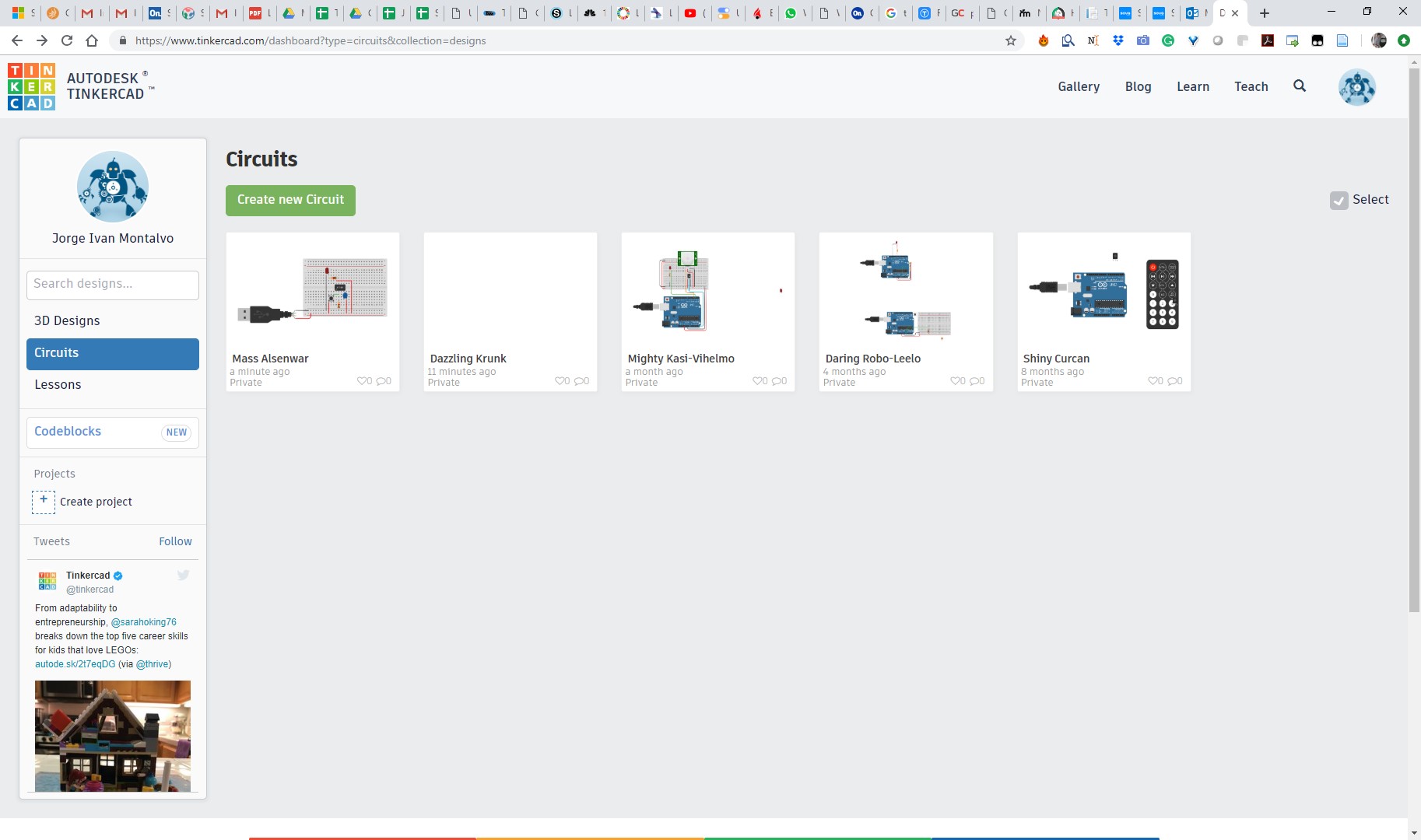
On the column on the right you can search for all the components, for this circuit, we need to drag and drop a protoboard, a capacitor, 2 resistors an LED, the ATTINY chip and a power source. Arrange all the components as shown below:
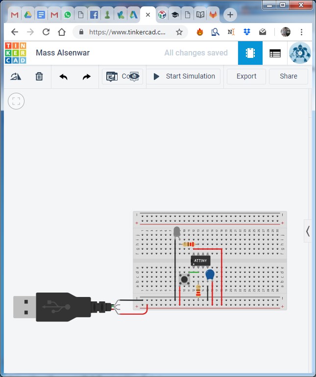
To rotate a component, you can use the first botton on the icon on the top, which will rotate it 15 degrees, and to change to create a wire, just click on an endpoint of a component and then on the point where you want to connect. If you need to change the color of a wire, just select it and then select the color. I personally like to have the power cables as red and the grounds as black, but this is up to you.
Now, click on the ATTINY and press the code button on the top right. By default, you see the block interface, change it to text, and type the following code. After it, Test the simulation by pressing Start Simulation. If you press the push button, the led should turn on. To make the led brighter and the easier to see, change the led color to white, and the resistor value to 220 ohms.
int led=2;
int button=3;
boolean state=0
void setup() {
// put your setup code here, to run once:
pinMode (led,OUTPUT)
}
void loop() {
state = digitalRead(button);
if (state==1){digitalWrite(led,HIGH);
} else {digitalWrite(led,LOW);
}
}
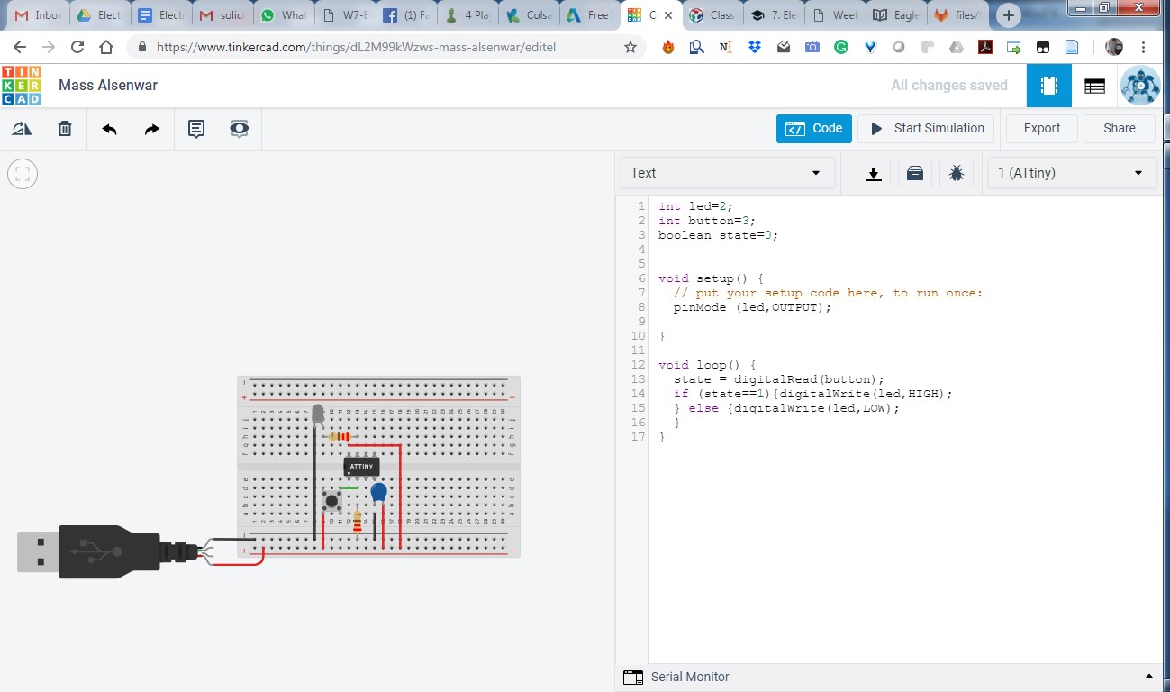
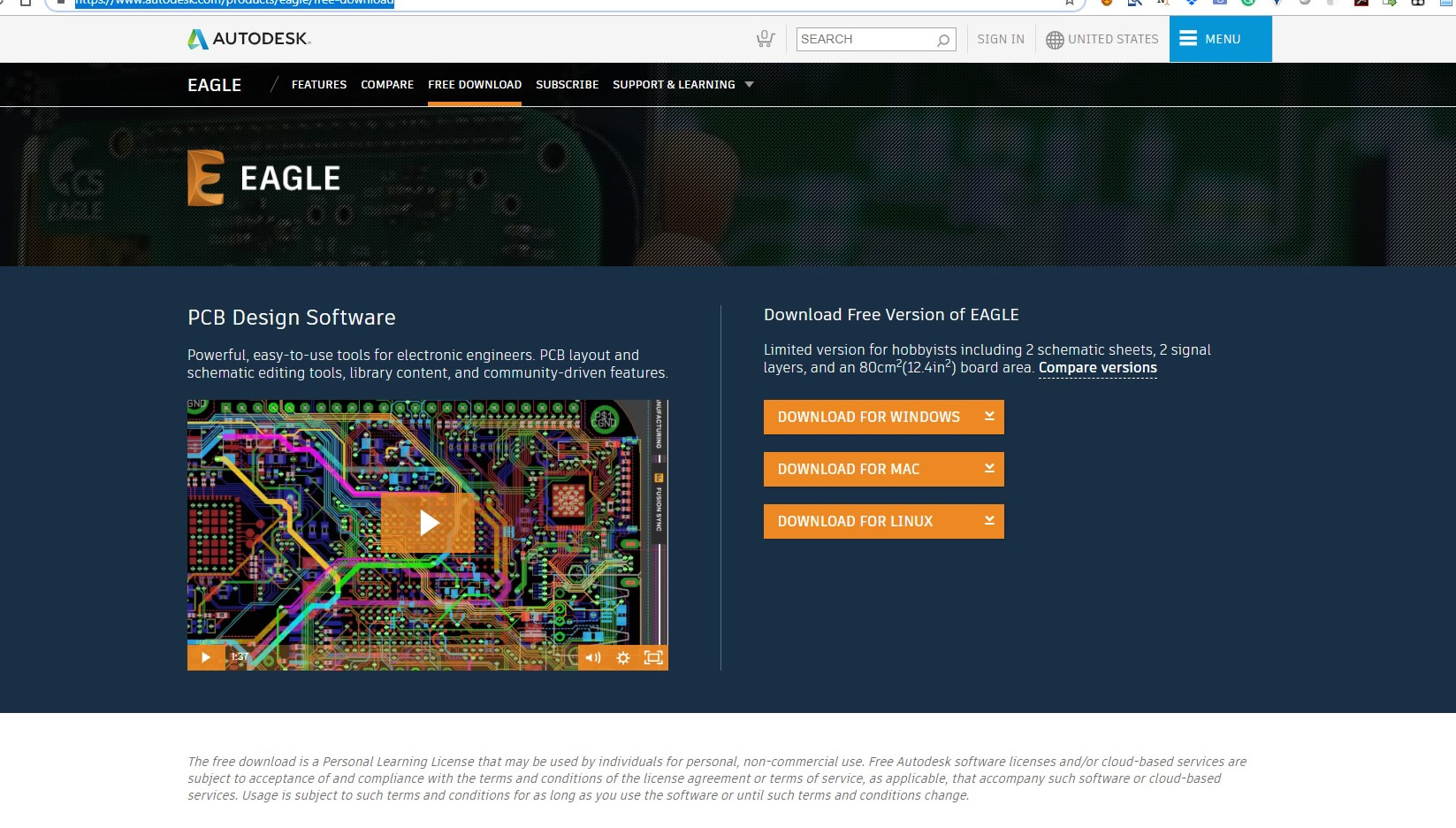
Now that the first simulation is ready, and we were able to test it, we need to create a pcb for all the components. For this, we need to jump to another software. We are using eagle. From Thinker CAD, you can download a file to start, by clicking in the export button. Now go to https://www.autodesk.com/products/eagle/free-download and download the installer for your OS.
After installing, the software, make sure to download and install the libraries available at https://github.com/Academany/FabAcademany-Resources/blob/master/SUMMARY.md
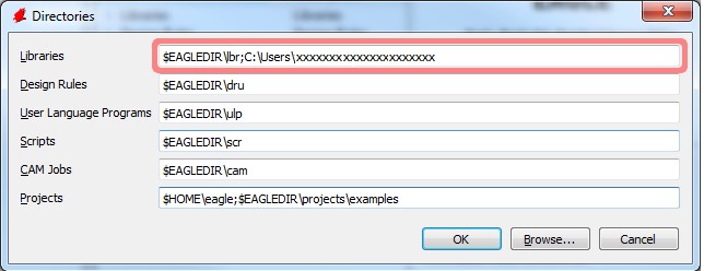
Just download the zip file, and in the main screen go to the "Options" menu and then select "Directories". This is a list of computer directories where EAGLE looks when it populates all six objects in the tree view...including libraries.
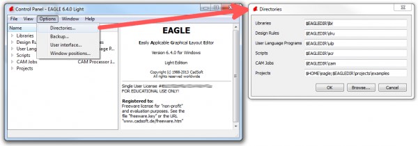
In the "Libraries" box is where you need to add a link to the directory where you saved the libraries. There are a few options here. If you'd like to keep the default libraries and add the new ones, add a semicolon (;) after "$EAGLEDIR\lbr", and paste the new Libraries directory location after that.
You can reuse a library of another board you have just by browsing for the schematic file, as sometimes in another project you have all the parts you need.
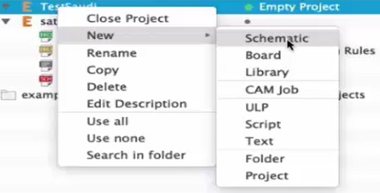
To start, create a new project, and then right click on it and create a new schematic.
To begin use the place component button and select the component you need from the library.
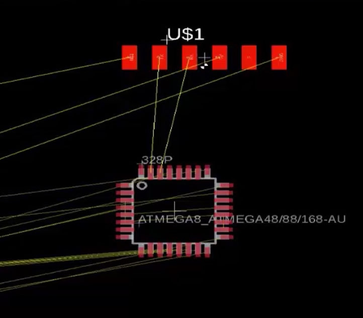
The first thing I will place is the Atmega.
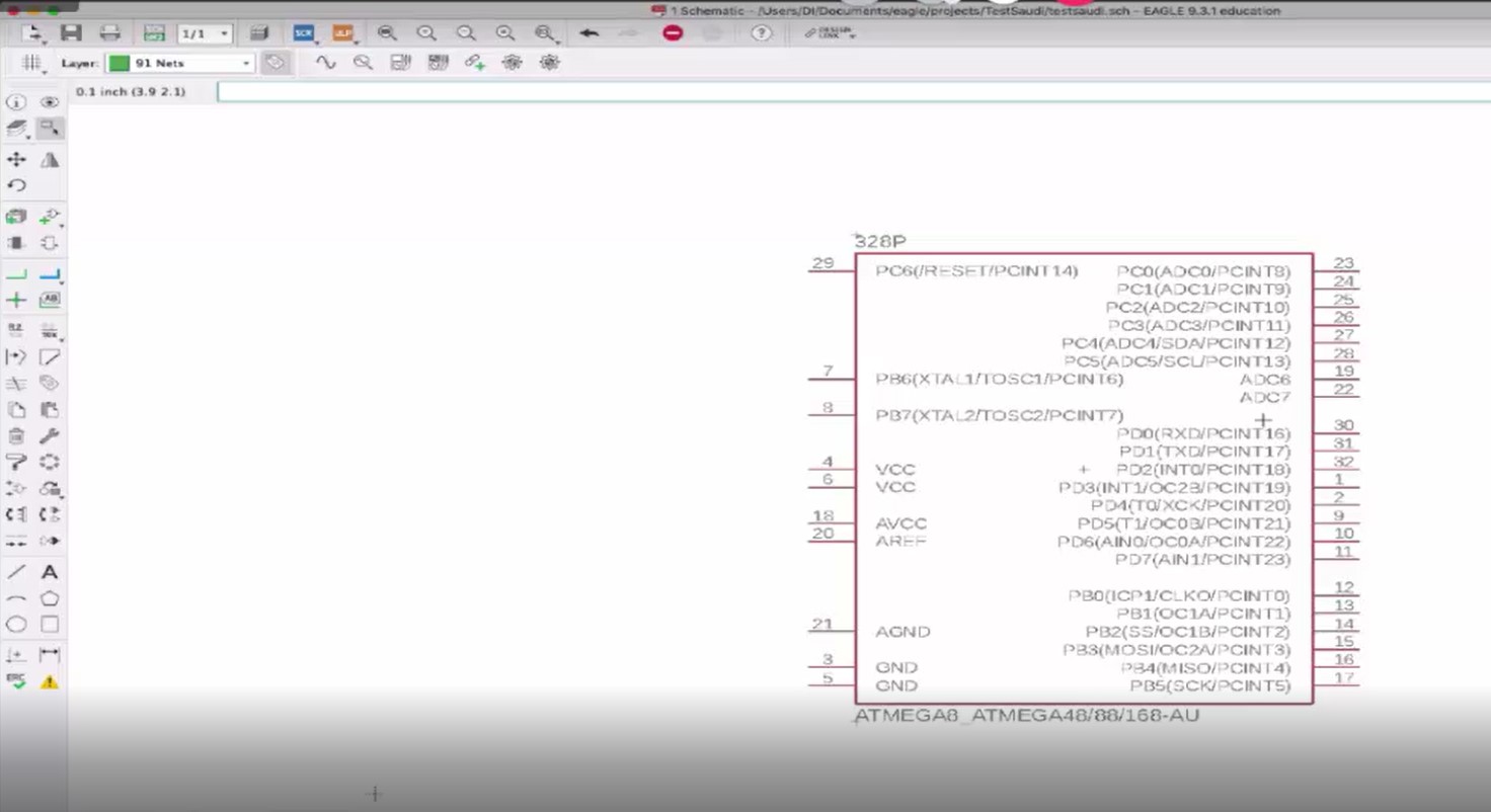
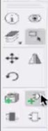
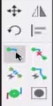
Now we can begin creating conections. For this, we need to use this button

To connect between points. As lines can become very messy, you can use labels to organize your schematic. For this, you can use the label button,

and on the top bar change to cross reference label
and just place the label with a name. Then, anytime you place another wire and use the same reference label, internally the points will be conected.
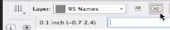
To begin, I will connect all the grounds to a Label called GND and all the VCC to a label call 5V.
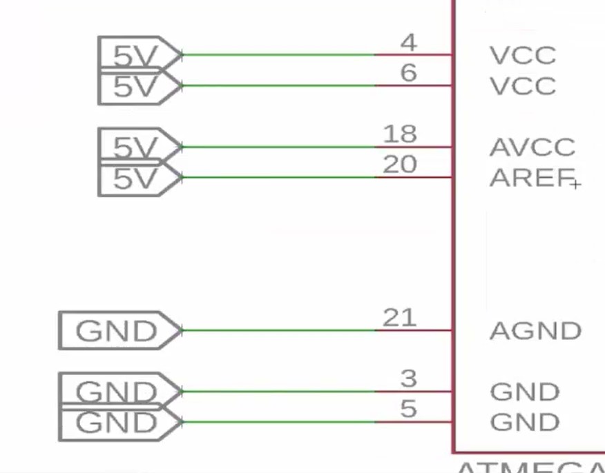
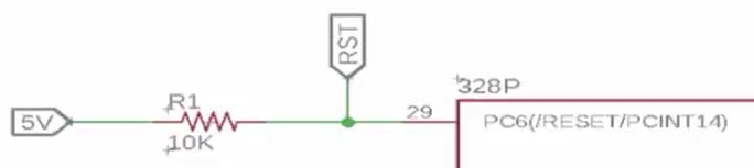
Next, I will connect the reset to VCC through a 10K resistor, To place the resistor, i just look for it in the library using the place component, and then right click and change value to modify the value I need.
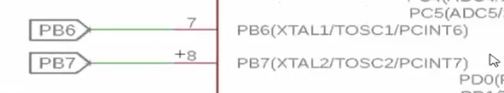
Normally, I would need to connect a crystal, but Here in saudi I could not get in time the capacitors required, so I will just connect these pins to two labels called pb6 and pb7
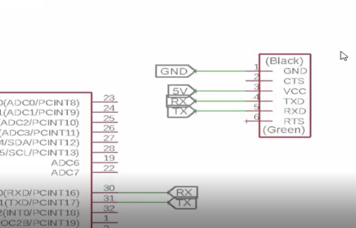
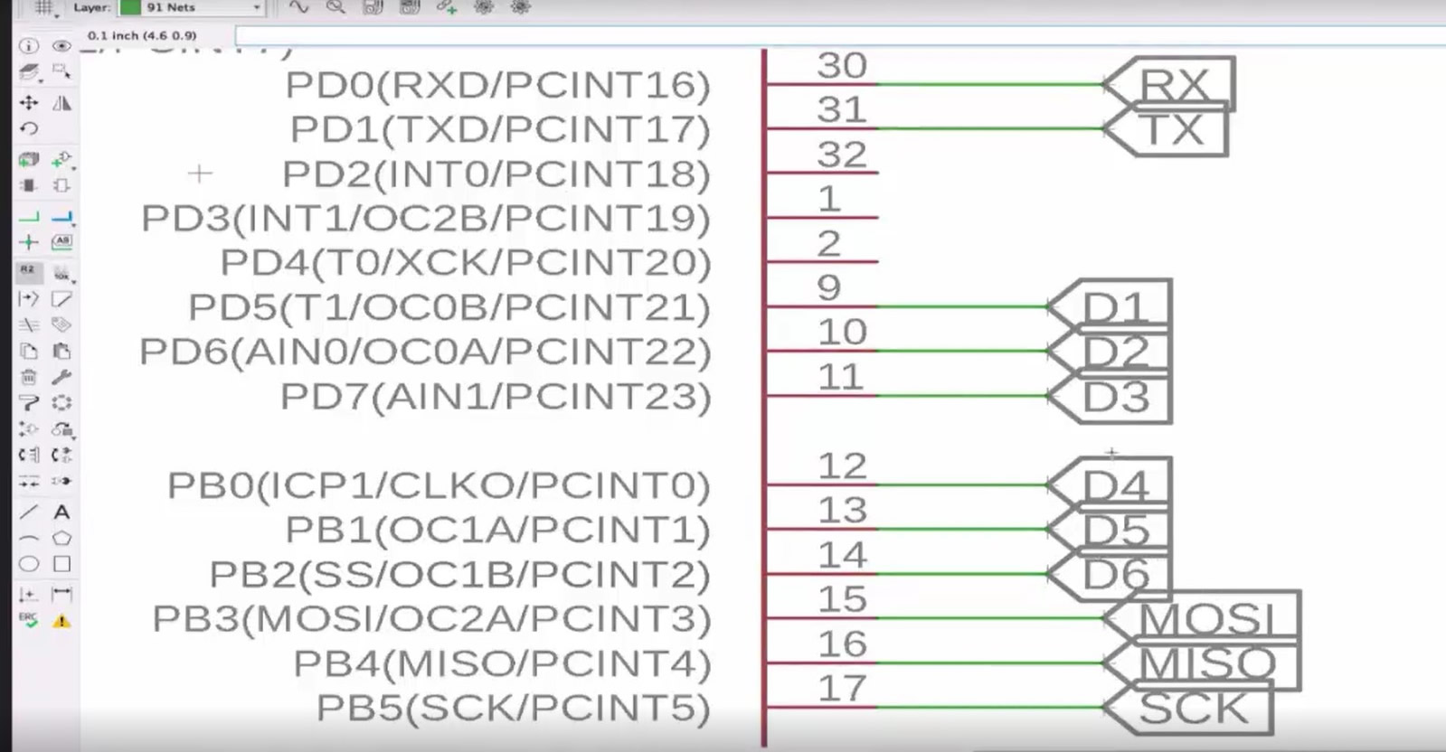
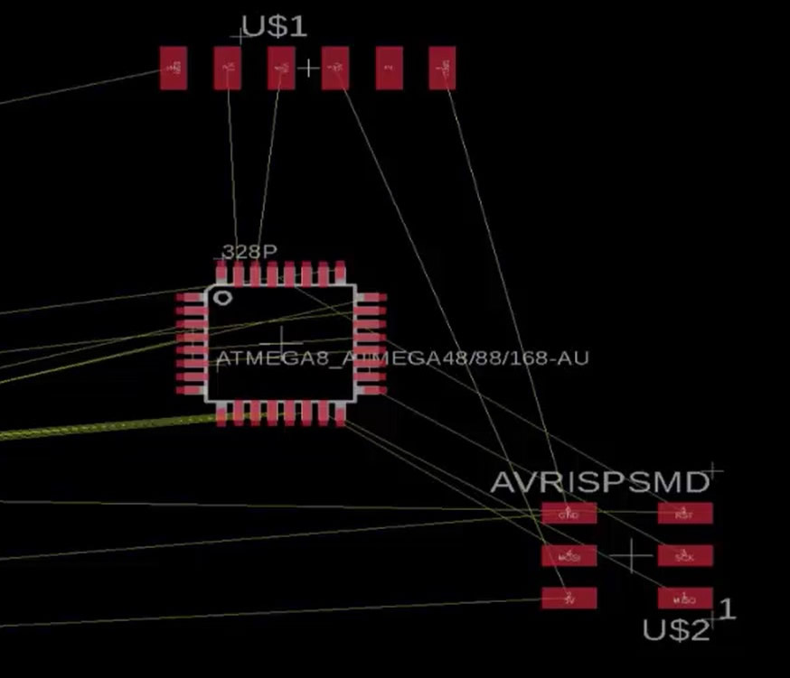
Now, I will place the FTDI connector and make the connections using labels. If you see in the Atmega, pins 30 and 31 are RX and TC, so need to connect them cross, RX to TX and TX to RX, as shown below
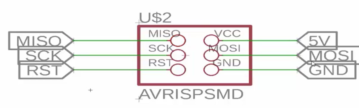
To connect the RTS, I nees to AVRISP, so I look for it in the library, place it, and then create labels to connect them.
And connect MISO, MOSI and SCK to pins 15, 16 and 17.
For the RST pin, You need to put a label in the RESET connection before the resitor, as shown below
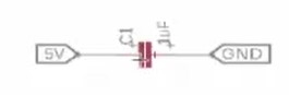
To filter the signal, we need to place a capacitor between vcc and ground, so I just place component, look for the capacitor and place a 1uF capacitor and connect it with labels between 5V and GCC
Now, the RST from the FTDI should be connected to the RESET of the Atmega through a 100nF capacitor. as shown below:
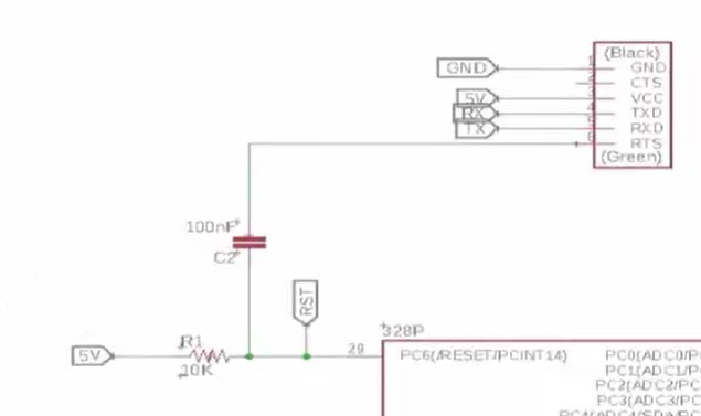
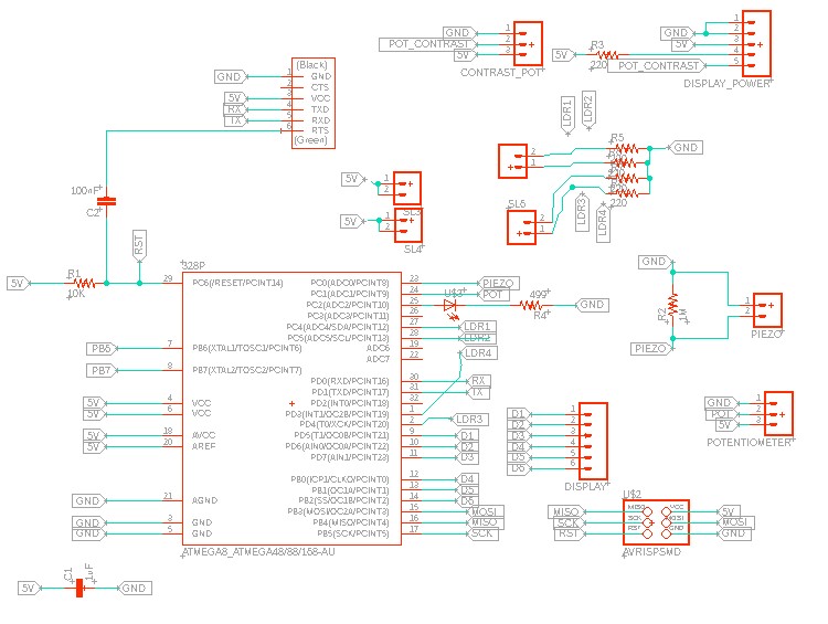
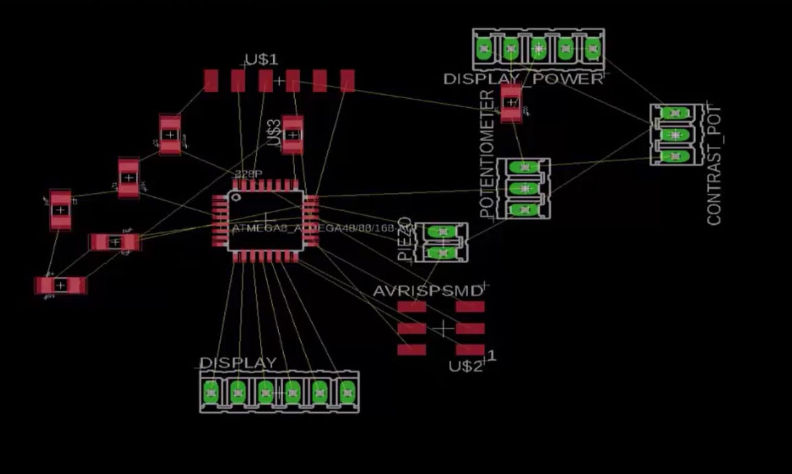
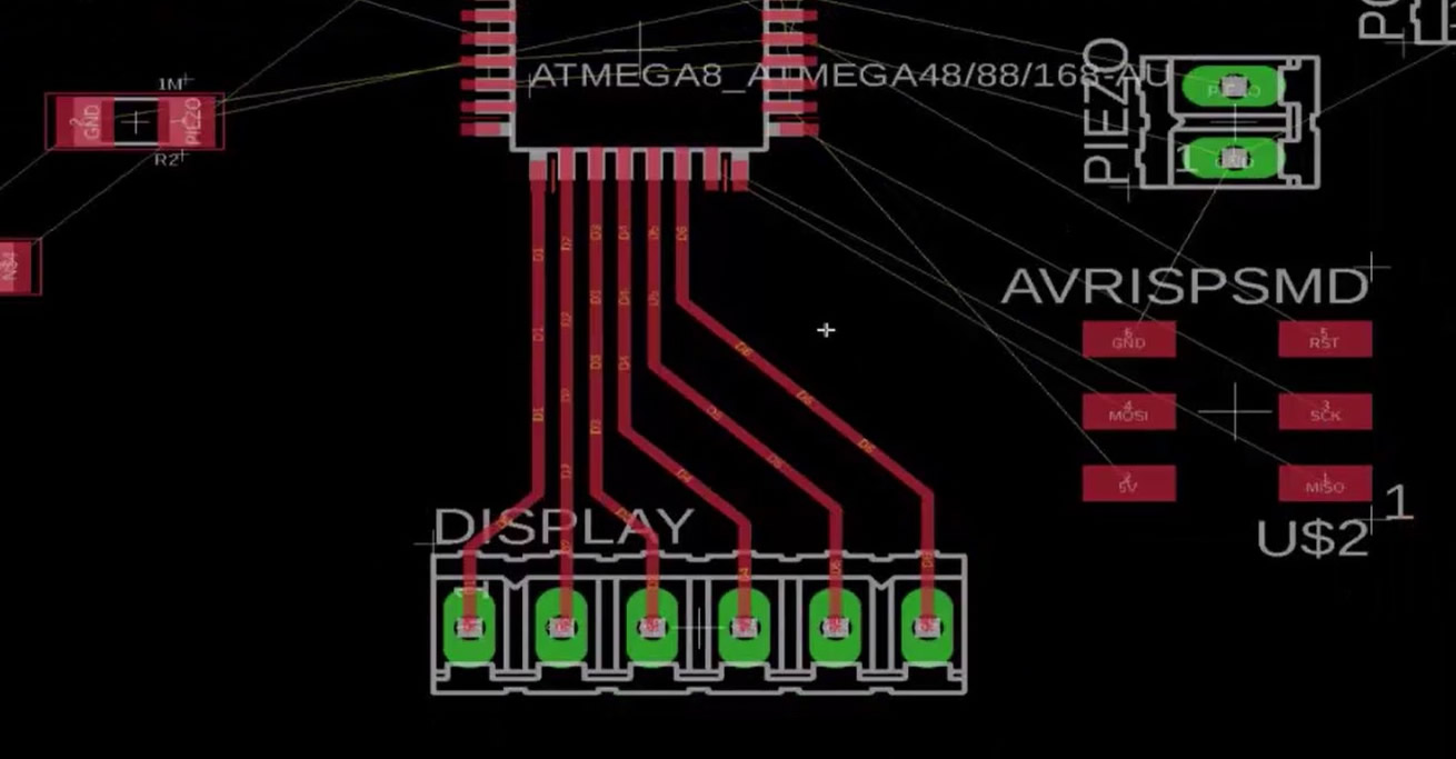
Up to this point, this is the basic connections needed to use the board as an Arduino. Now, I will connect the inputs and outputs I need for my Project. The first output I will use is an LCD screen. For this, I need 6 data pins, so I will place an M06 conector, and change the name for Display, and then connect the pins using labels to pins D1 through D6 as shown below:
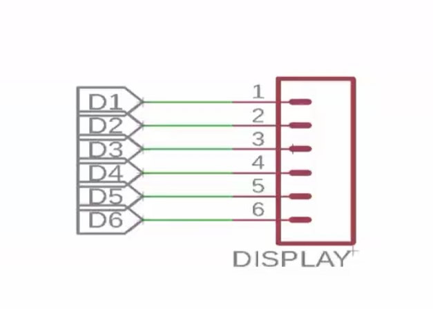
And then, in the Atmega, create the labels in the pins 9 through 14, as shown below
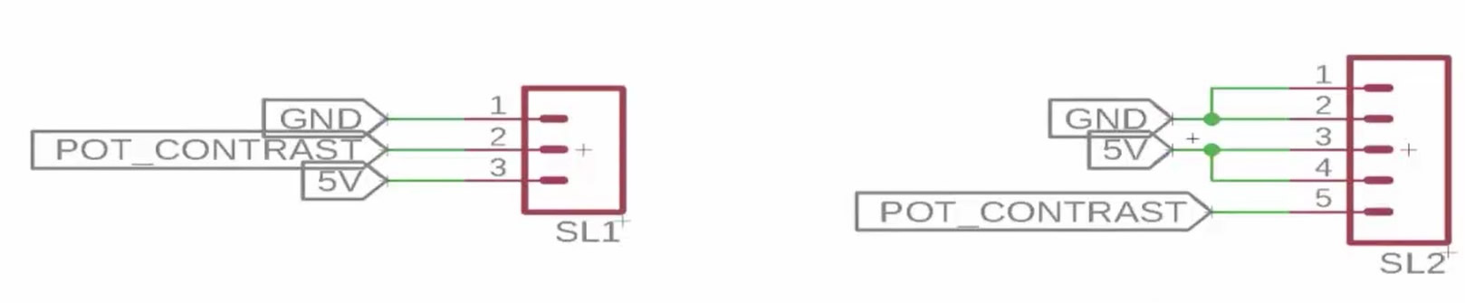
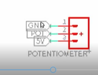
Now, for the power we need 2 vcc and 2 grounds, and for the contrast, we need a potentiometer. So I will place an M05 connector, and place connect 2 vcc and 2 grounds, and a potentiometer signal, and then place and M03 conector, to place my potentiometer to vcc and ground, and then take the middle signal to the display, as shown below:
As another input, I will place an M03 and coonect GND, VCC and another POT, which in this case I will connect to pin number 24 in my Atmega.
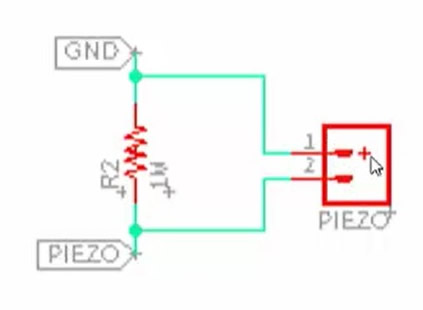
As another Analogue input, I will place an M02, and connect in parallel to a 1M ohm resistor between GND and VCC, and connect the label to pin number 23 in the Atmega.
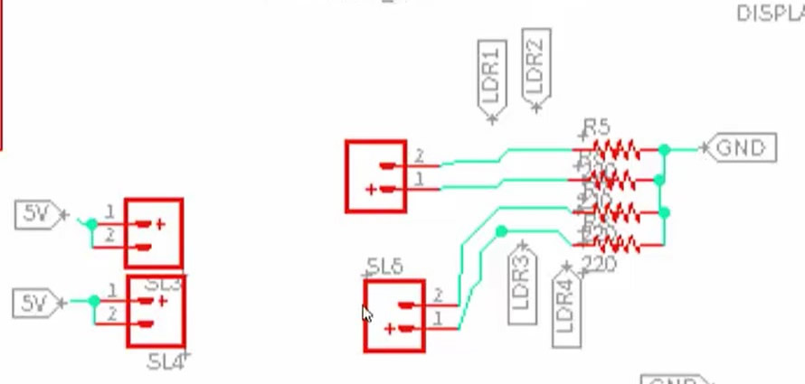
As the main inputs of my Final Project, I need to connect 4 LDRs, that will be connected using a voltage divider with resitors. for this, I placed 2 M02 conectors, and connected them to 5V. Then, another 2 M02 Connector and connect them through 4 resistors to Ground, and then create labels LDR1, LDR2, LDR3, and LDR4 before each resistor, to connect them to pins 1 and 2, to be used as digital inputs, and to pins 27 and 28 of the Atmega to be used as analogue inputs.
Finally, as a second output, I placed an LED to pin25 of the Atmega.
![]()
With this, my schematic will be ready, and I can begin 2nd part of the board which is placing the component in the board and creating the routes. This is the complete schematic of my final board:
Now, I will press the switch to board button on the toolbar:
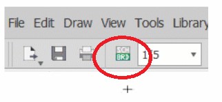
And I will see all the components I need to place.
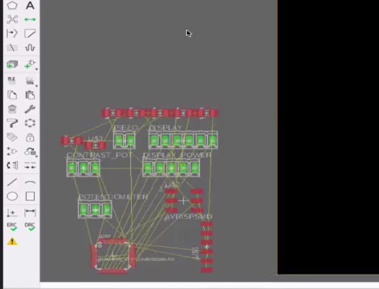
All the component are outside, and I need to place them in the black area. The first step will be moving the microcontroller. For this, I use the move button

and then click on the microcontroller, and then click again where I want to place it.
Now, I need to begin moving the rest of the components, to have as many direct connections as possible. I will begin by moving the FTDI connector. This one I will place above the microcontroller, because the connections will be direct, as shown below.
Now I will move the ISP connector. As seen, we have 2 connections to the FTDI, and 3 on the lower part of the Atmega. To make it easier, I will place it in the lower part.
Lets take a look at the connections. If you see, there are now yellow lines connecting the ISP to the FTDI. If we press the ROUTE NEST button, It will simplify the connections, as so many points are common.
See how the connections changed after clicking this button. Now its easier to connect.
So following this logic, I start placing all my components so that connections are as simple as possible
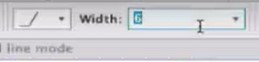
Next, I can begin drawing my routes. for this, I use the route button
adjust the width on the top to 14, and then click on the points I want to connect.
I will begin with the display as the connections are very direct.
Following these same steps for every line, the software will help you find the best routing connection for all the components. At the end, I arrived to this design:
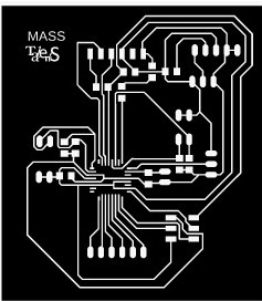
Which can be exported as DXF, SVG, or PNG, to be taken to the Carvey for Fabrication.
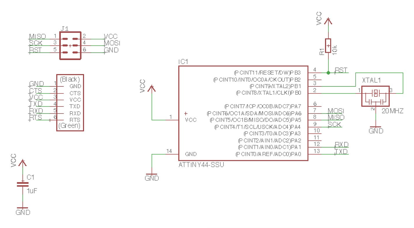
# Also for this week, I will do start by analizing the hello world Board. The original board schematics looks like this:
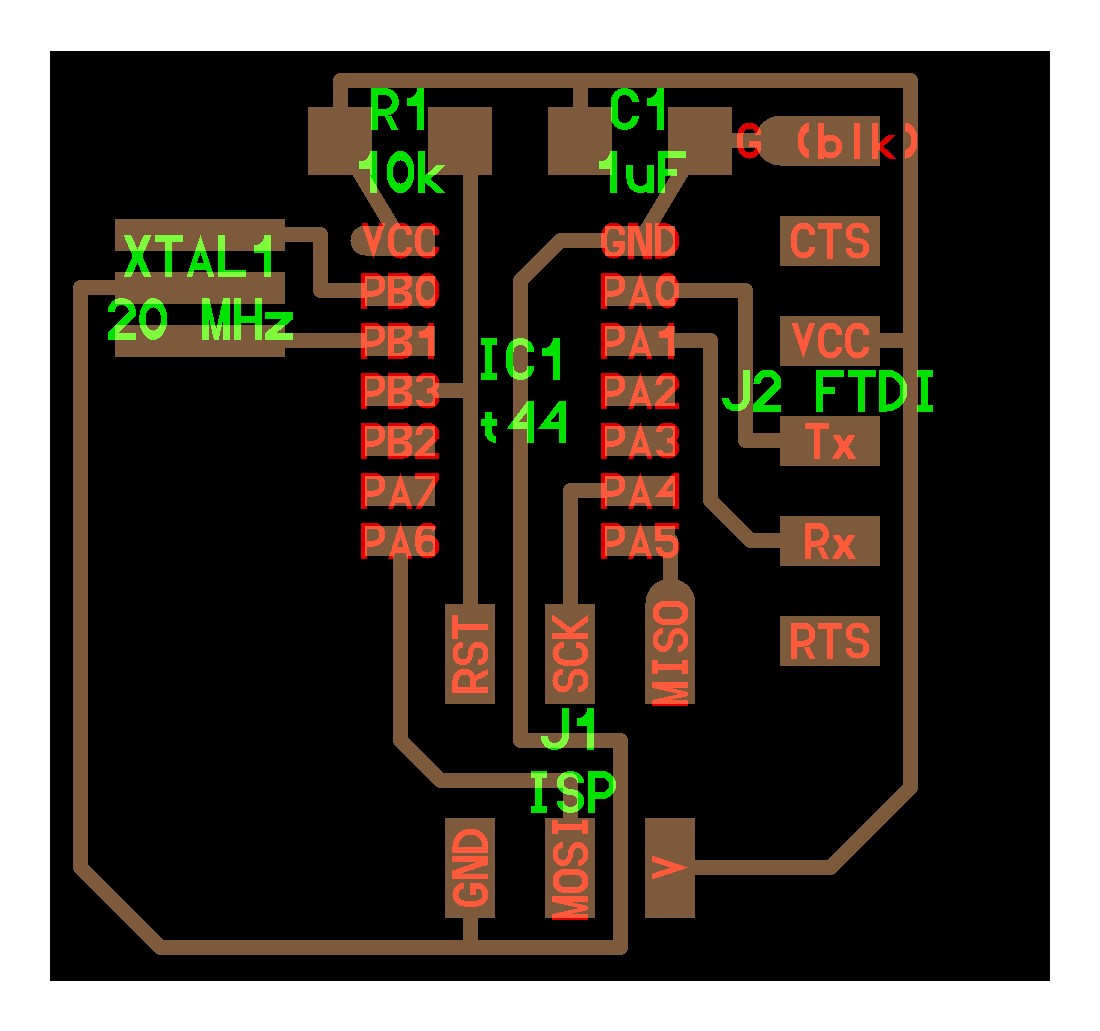
And the board looks like this.
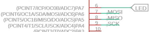
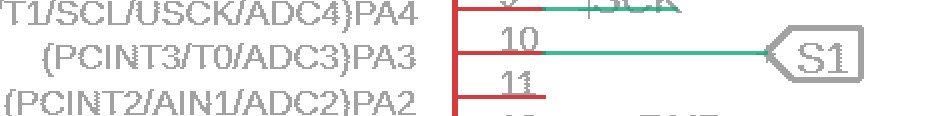
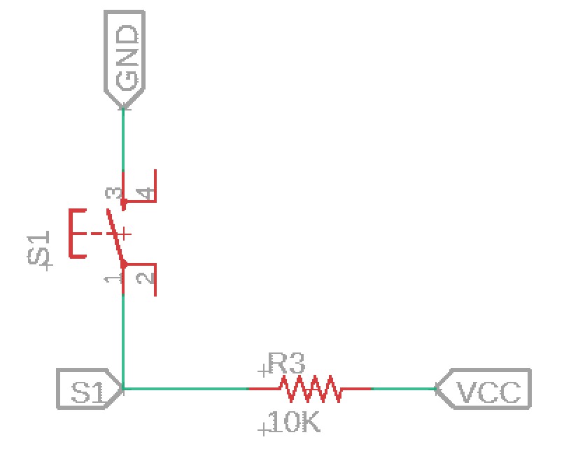
As seen, it uses an ATTINY44 and it has the FTDI connector, an external crystal, and has some extra pins to be used as required. In our case, we will use Use pin 10 on the to connect to a button and Use pin 6 on the to connect to the LED.
For the led, I just add a connection and a label named LED on pin 6, and then place a 499K resistor and an LED, and connect it between LED and GND
![]()
And for the Push Button, I create a connection and call it S1 in pin 10
And then place a push botton and a resistor, and connect them in series between ground and vcc as shown below. Then, a label s1 I send to the pin 10.
Now, I'm ready to begin my board, I switch to the board interface and try to place the components.
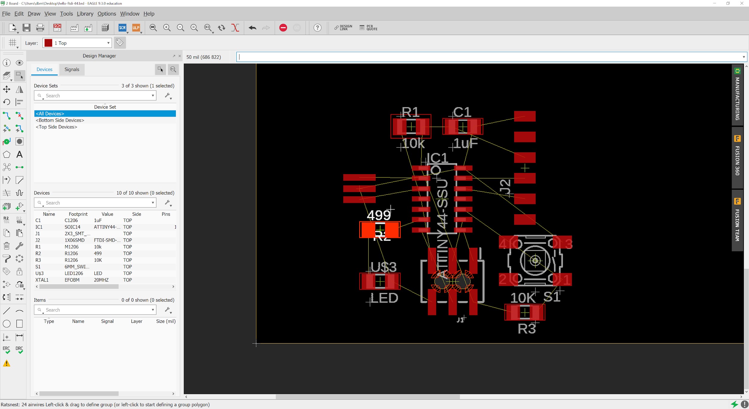
After a lot of placing, this is the best connection I could do
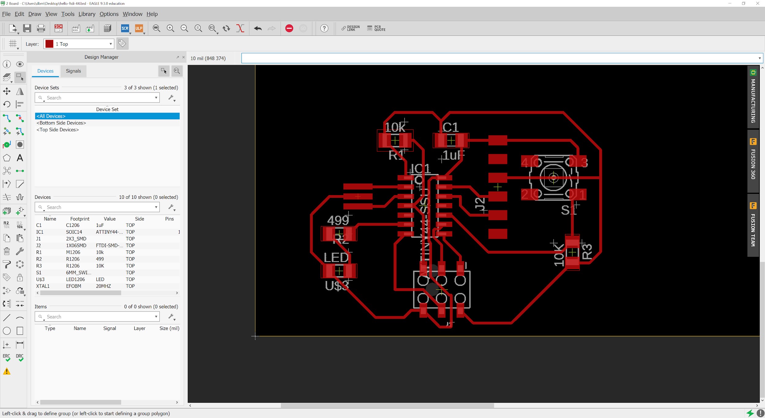
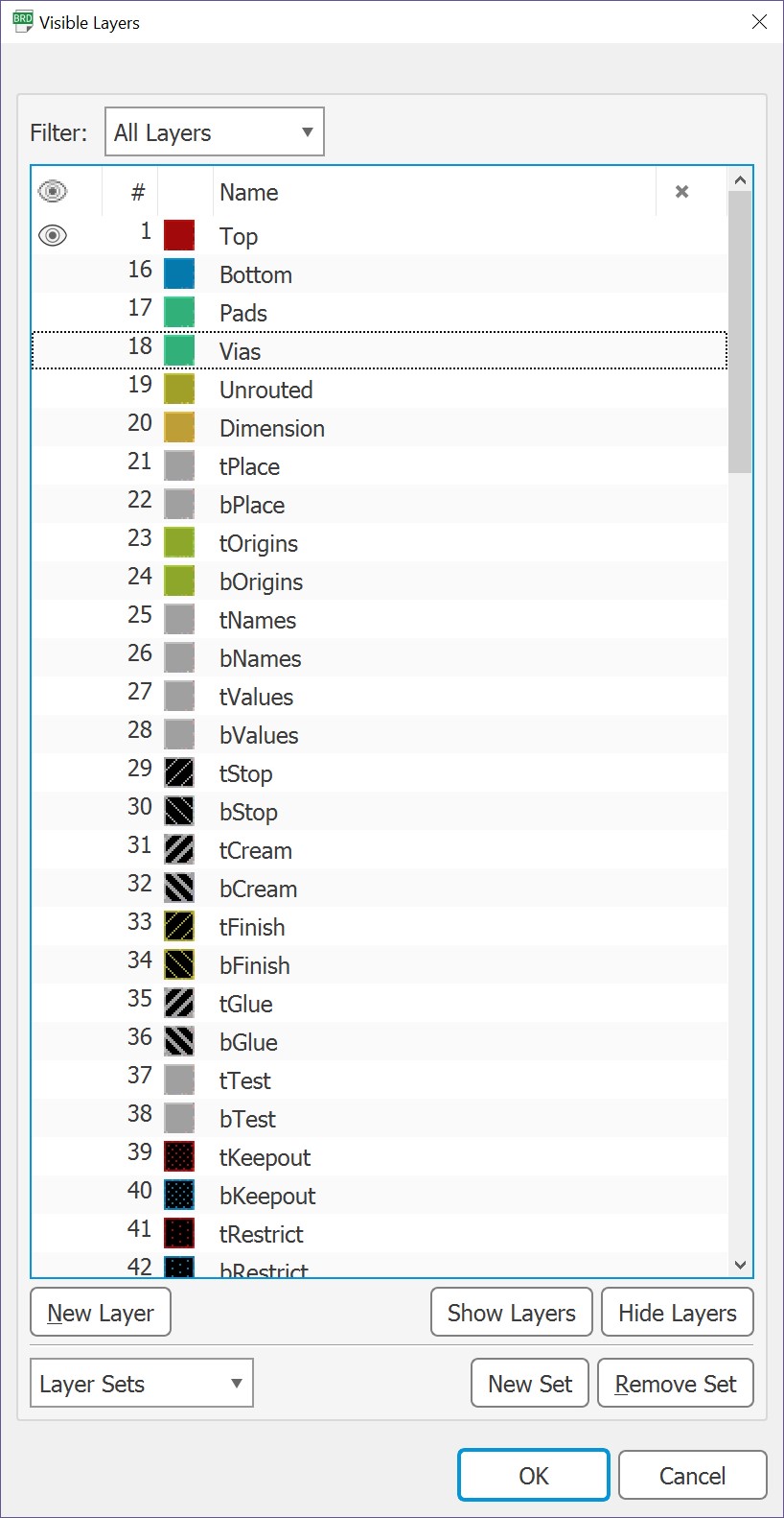
So, after checking all the clearance problems, I'm ready to export my traces for routing. I open the layer settings and only turn on the top layer
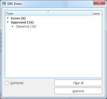
It is very important to you check the DRC-Settings, these make sure the board can be manufactured with no problem. For milling the board I’m using the inventables carvey with a 1/64 inch end mill for the traces, and for the outline 1/32 inch.The DRC-Settings I'm using is from the FabAcademy.
DRC helps you check that the end mill go between traces and pads and makes sure no lines are overlapping. DRC showed some problems so I had to move my traces to correct the errors shown. Please check the link to download my settings here.
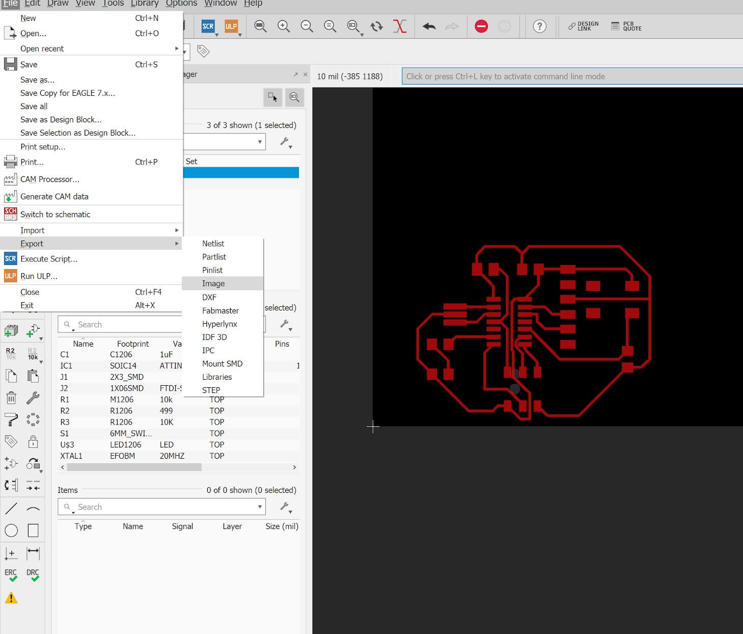
Now I'm ready to export the file.
And then go to file → Export → Image
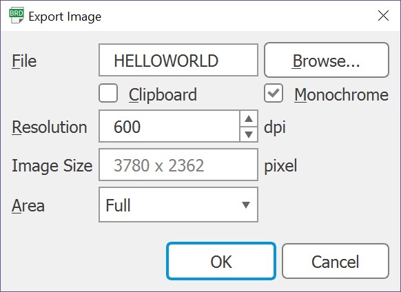
And export the image in 600 dpi as monochrome
Then, I can open this image in Inkscape,
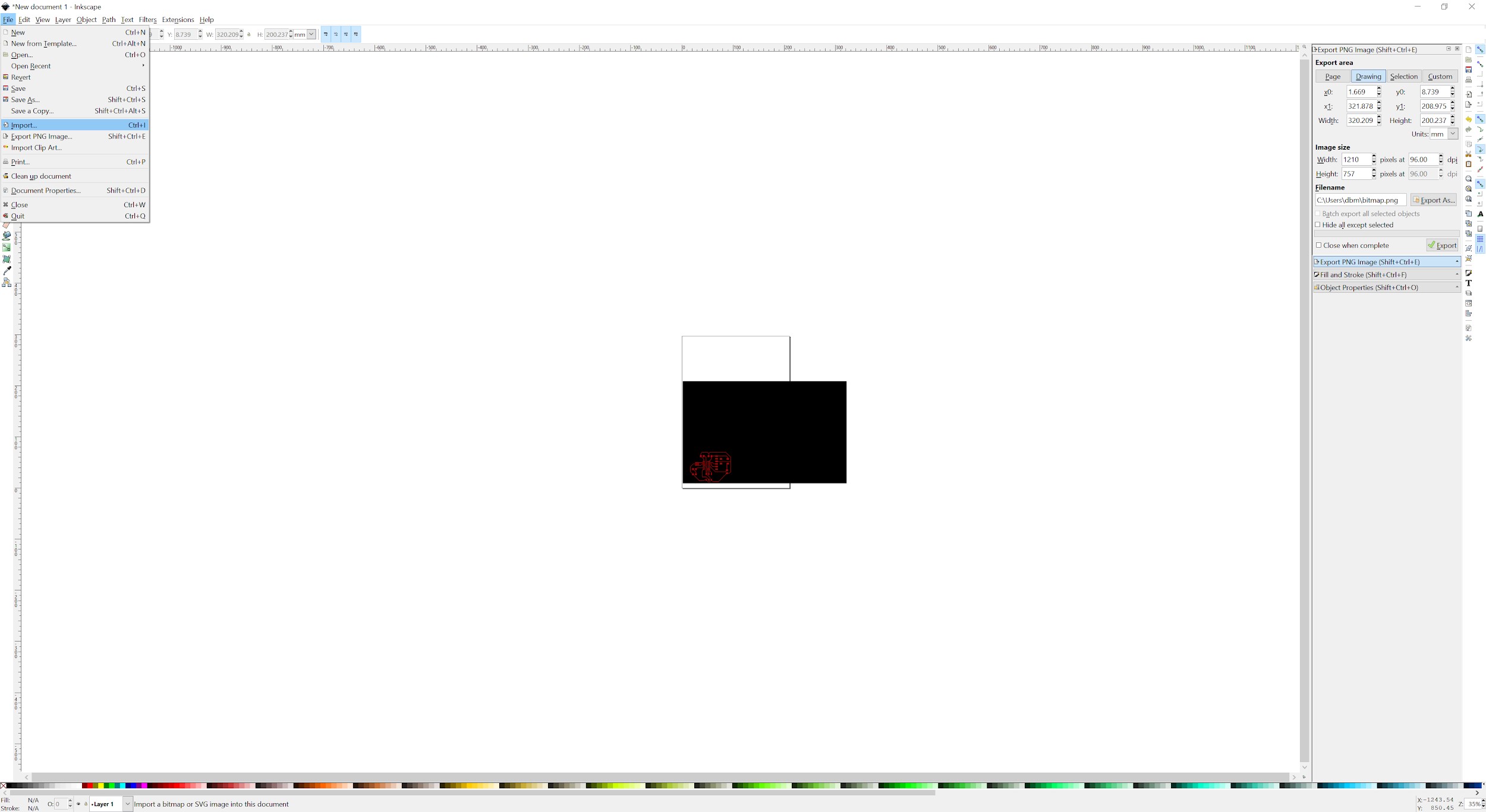
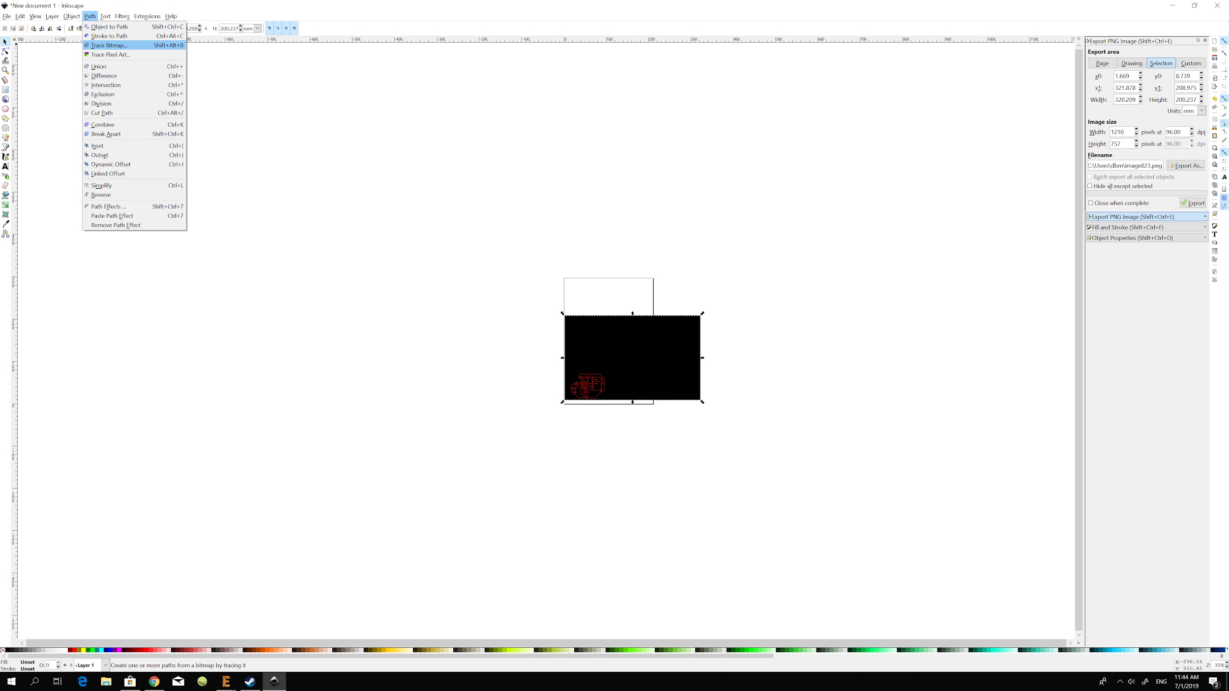
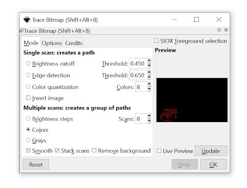
And then go to Path → Trace Bitmap
Trace It,
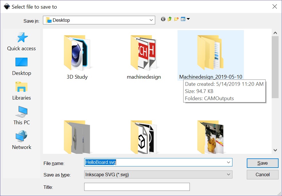
And then save as SVG to be able to route.
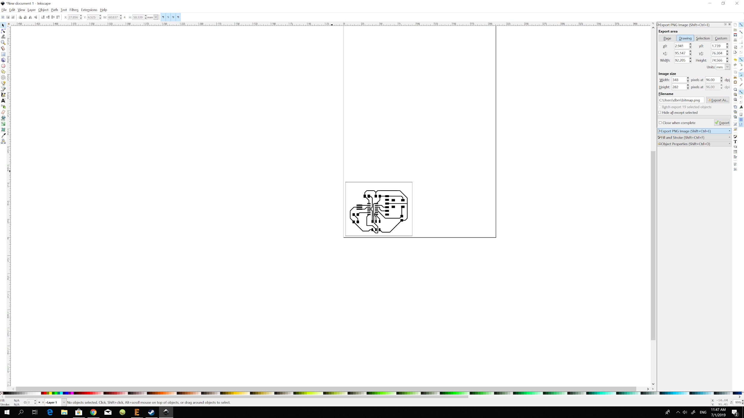
Finally, I just save as SVG
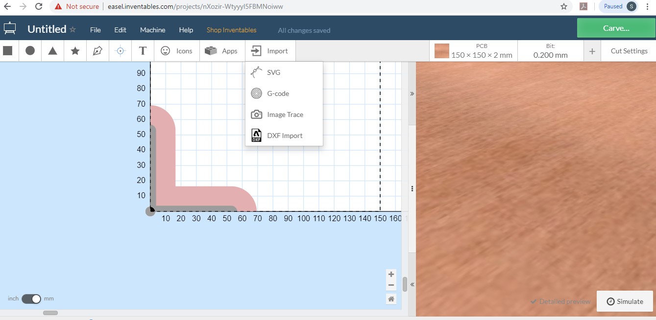
And Im ready to route. For Fabrication, I will use the carvey.
I open the software interface and import the svg
Set my milling to be 1mm depth, just enought to clear the copper from the board.
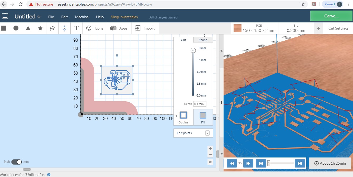
And select the proper end mill for pcb production
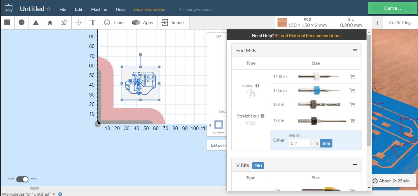
And now, set the settings for production
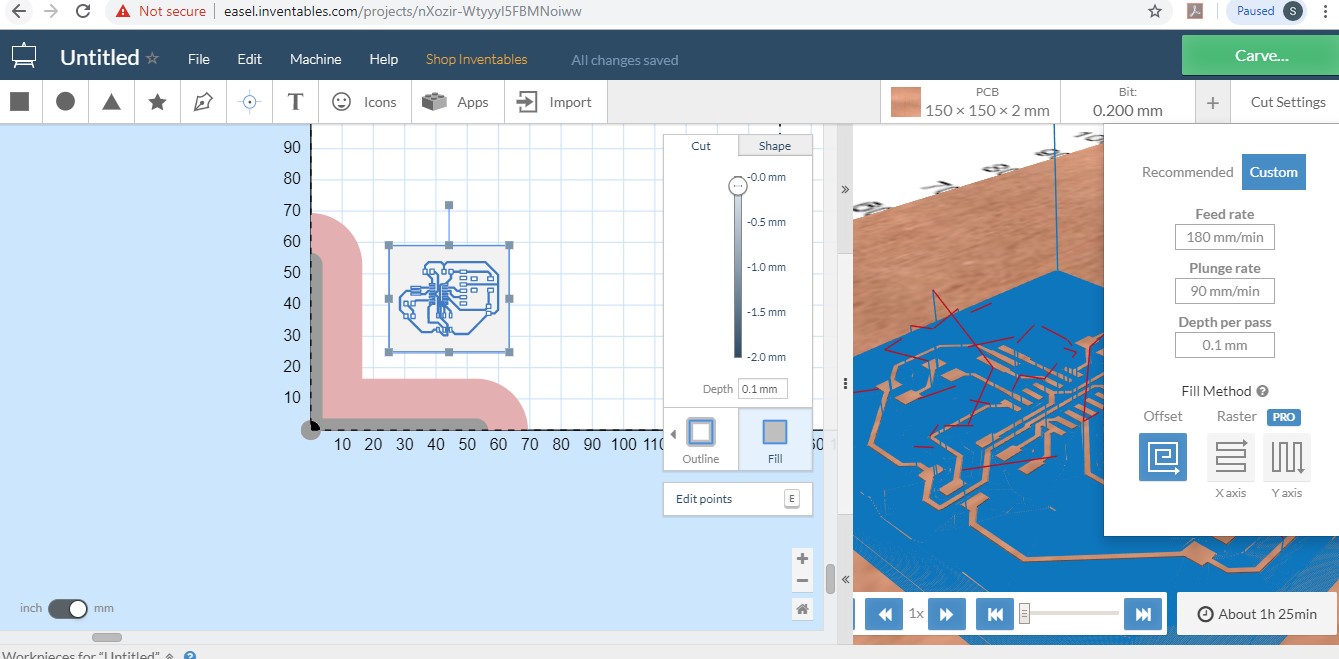
The feed rate will be 180 mm/min, which is 3 mm/s, the plunge rate will be half, 90 mm/min, and for the depth per pass, I will remove all material in one pass, 0.1mm. Now, I send the code to my machine and start the milling process
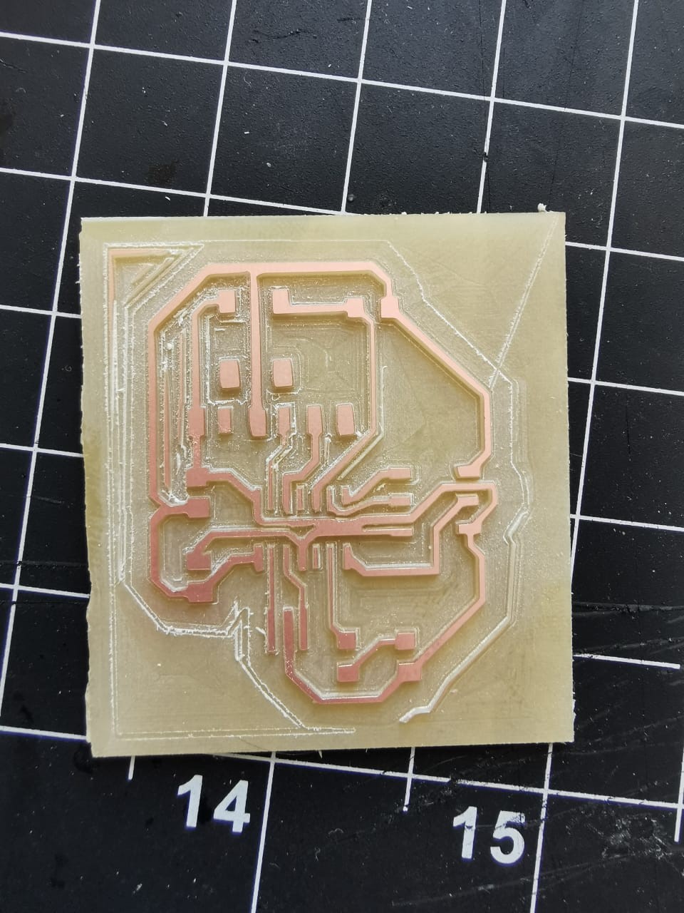
This was the final result after milling,
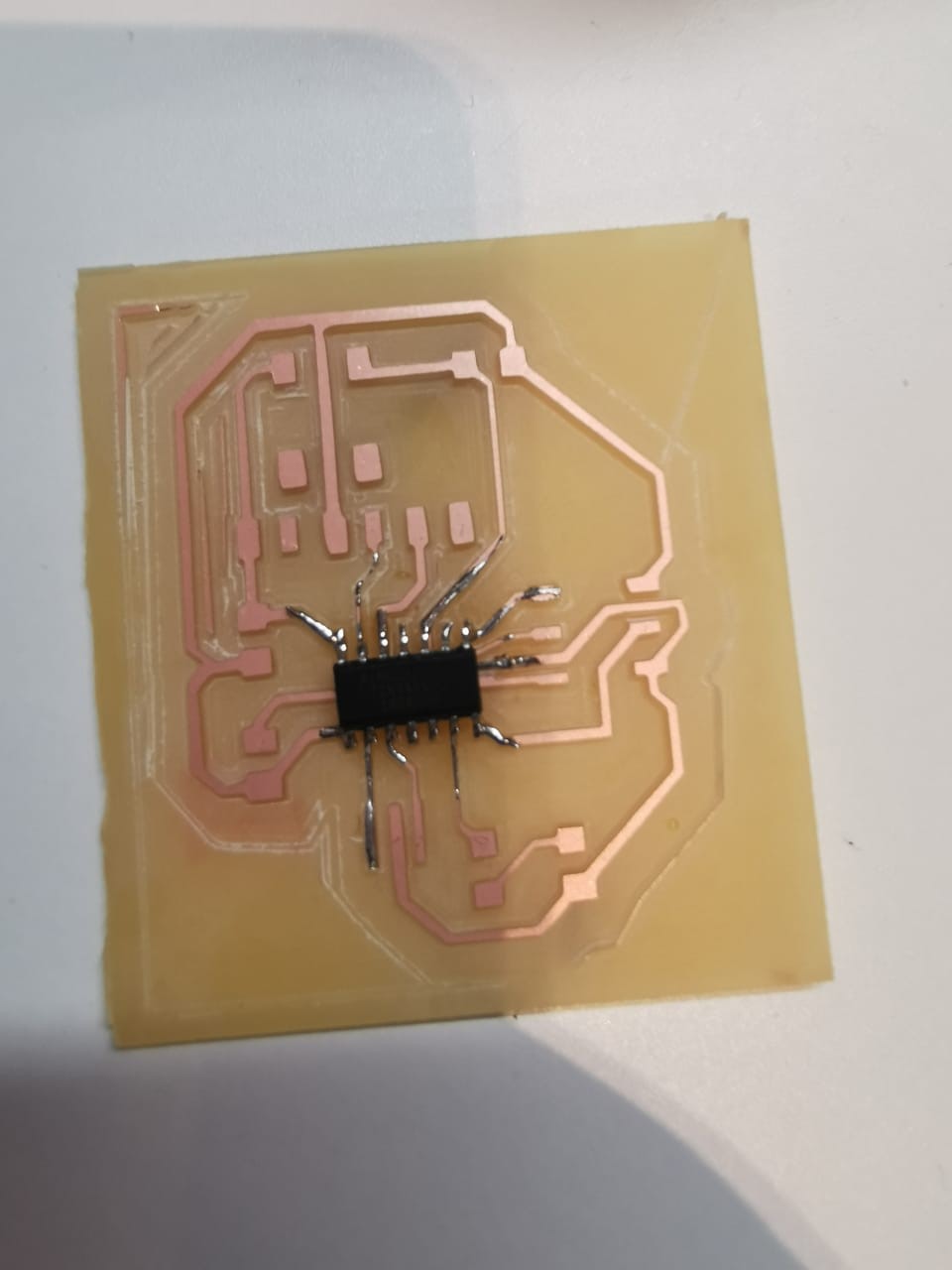
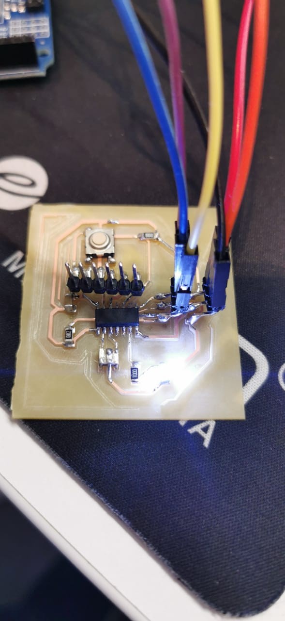
Now, the hardest part for me, soldering. In the previous boards I had made, I always made several to try to test the soldering and finally select the best result, but for this one, I decided to only make one, to push my self to be very carefull and try to get the best result. The first thing I soldered was the attiny.
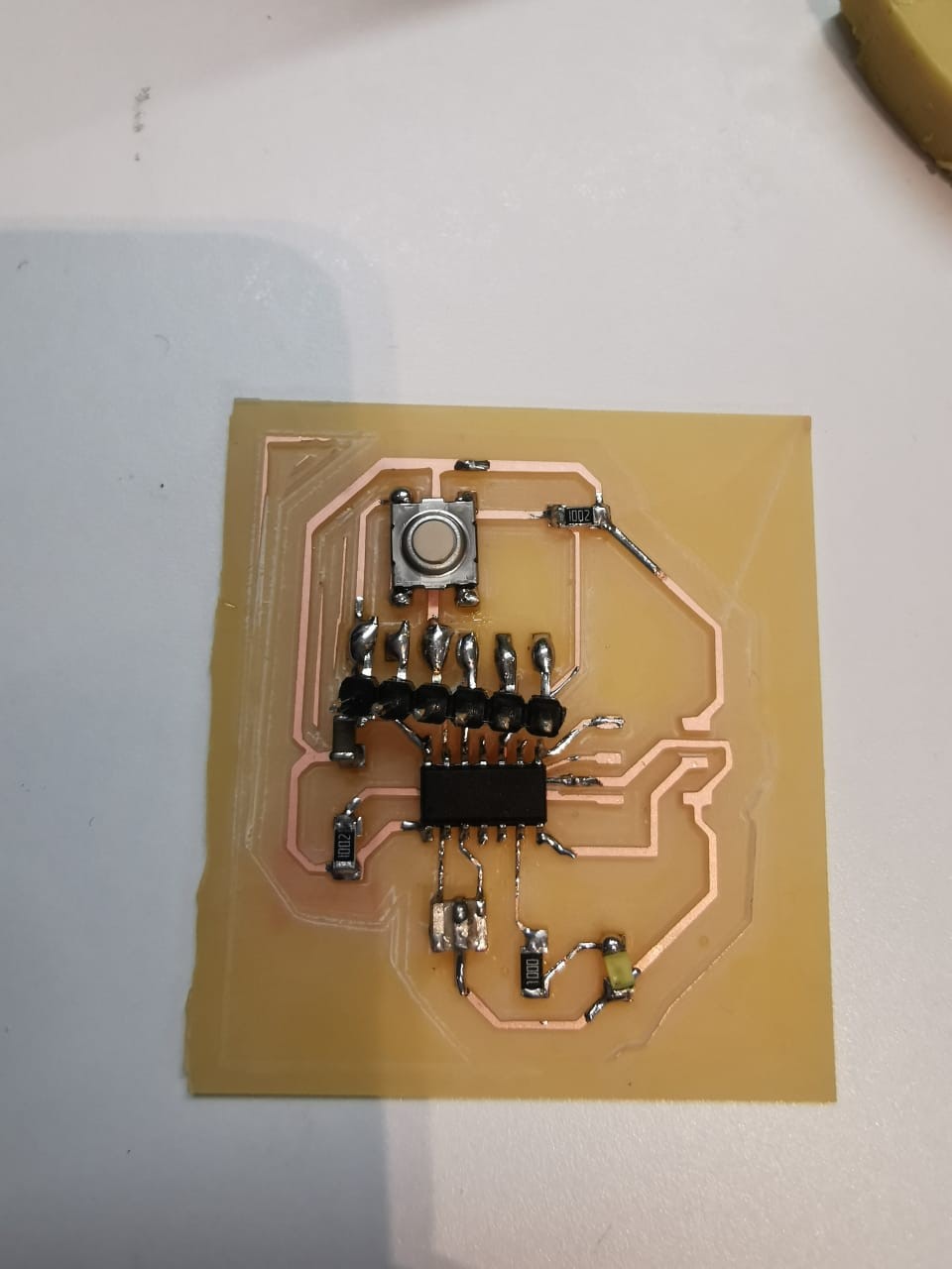
Then, I soldered the rest of the components,
And now, I was ready to test it. For this, I had to use an Arduino as an external programer, by conecting the pins in my board like this:
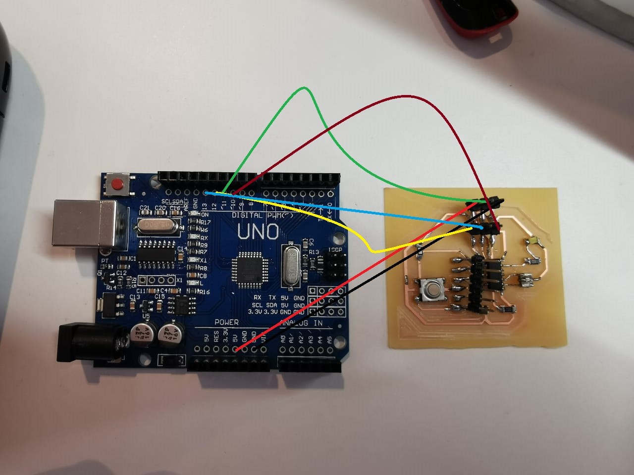
Then I connected the cables and tried programming my board.
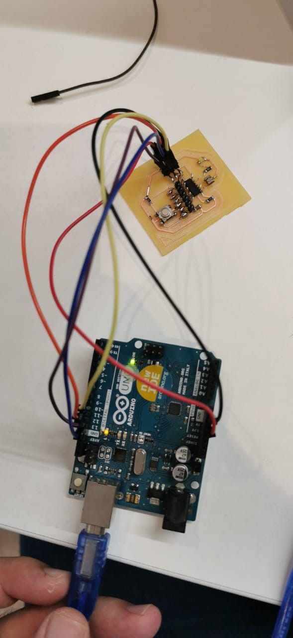
And to test it, I tried downloading the blink Program. I was very happy and excited to see it worked on the first try. This means the practice I had in the other boards help me alot and even though I still have a lot to improve, especially in my soldering, I'm very happy with the result!
Download File: the board design file ZIP
Download File: the Hello board design file ZIP
Download File: the blink code file ZIP