Week seven: Electronic design
Individual assignment
For this task, we have to make a new electronic board based in the "Hello World" model. But to design, we have to know how electronic components work. For this reason, i had to read tutorials about this subject.
Components
I found this and more information in this tutorial
Also, i measured the value of resistors and capacitor to compare with the standard values.
499 ohms resistor
1 uF Capacitor
Software
I downloaded Eagle software and Fab library following a tutorial, because i had to make a board using SMD technology.
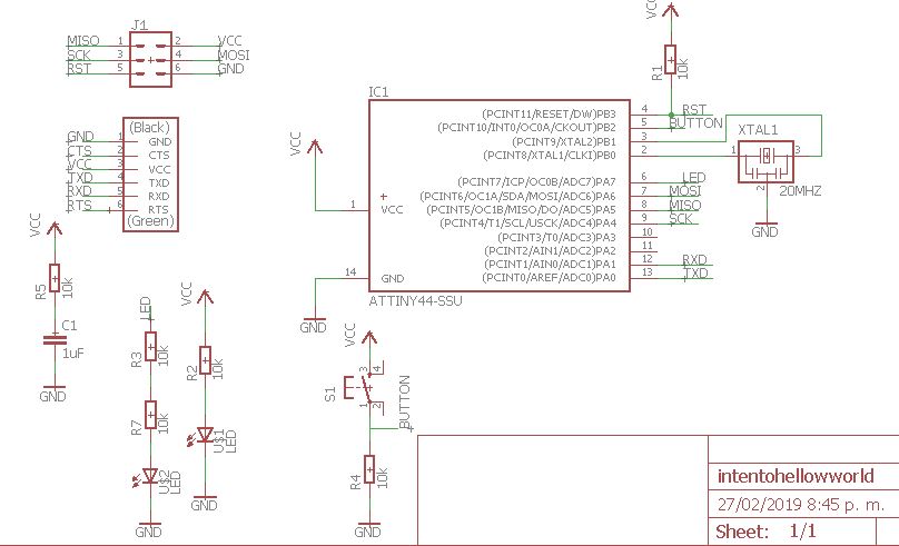
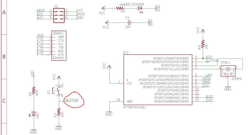
When you start a project in eagle, you start with the schematic design, in this environment, with the add command, we will add the components that we want to put on our electronic board, and the connections are made, it seems to me more orderly to use labels to connect, so I avoid knots or get lost. If the labels have the same name the components that have them will be connected, this also applies with the symbols of power source, in my case VCC and GND, all these pins are connected to each other.
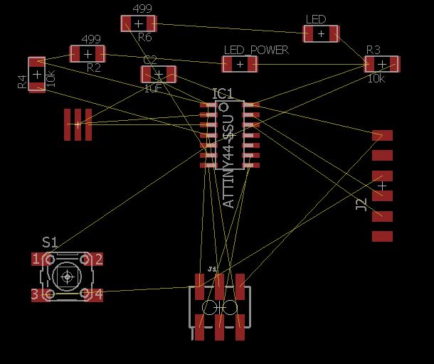
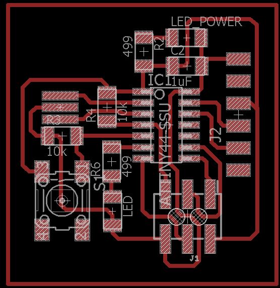
In my case, first i saw the schematic version of "Hello World" board, and added a button as input to Attiny 44, 1 power led connected to VCC and GND, 1 led as output to Attiny 44. 2 resistor of 499 ohms, 2 of 10k ohms and 2 of 0 ohms and made the connections using the wire tool and the labels that I mentioned previously.
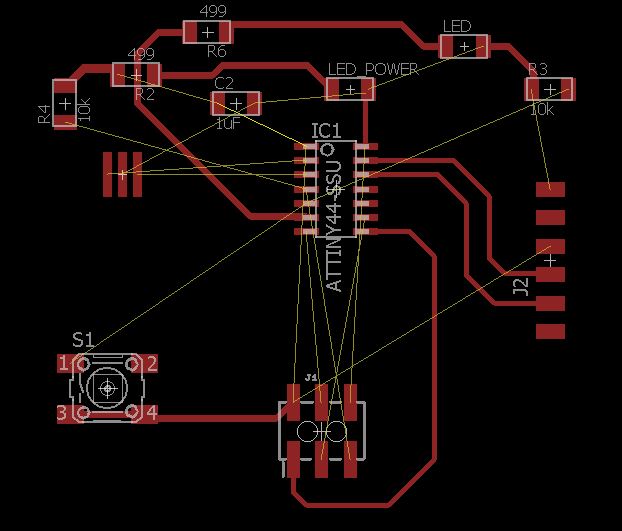
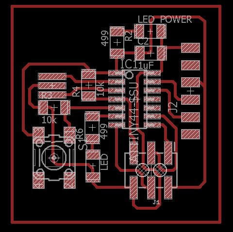
Once the schematic design is finished, it is passed to the board environment, which depends on the schematic, that is, each component that was selected in the previous design will be present in this environment with its real size dimensions, and this environment also has guidelines yellows that also depend on the connections of the schematic design, in order to properly design the board with all the connections, the components must be placed in such a way that it facilitates the tracing of the tracks, then with the route tool the path is traced where they will be the physical tracks, that is to say the copper, for this reason it is important to dimension the width of this.
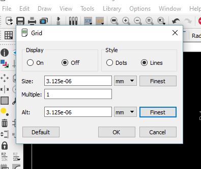
I adjusted the grid and I gave it finest in millimeters, I use 0.6 of width for the external tracks and 0.4 for the internal ones that connect to microcontrollers or components little ones.
Here I placed the components where I thought they facilitated the tracing of traces
In this attempt you can see the difference of the width of traces

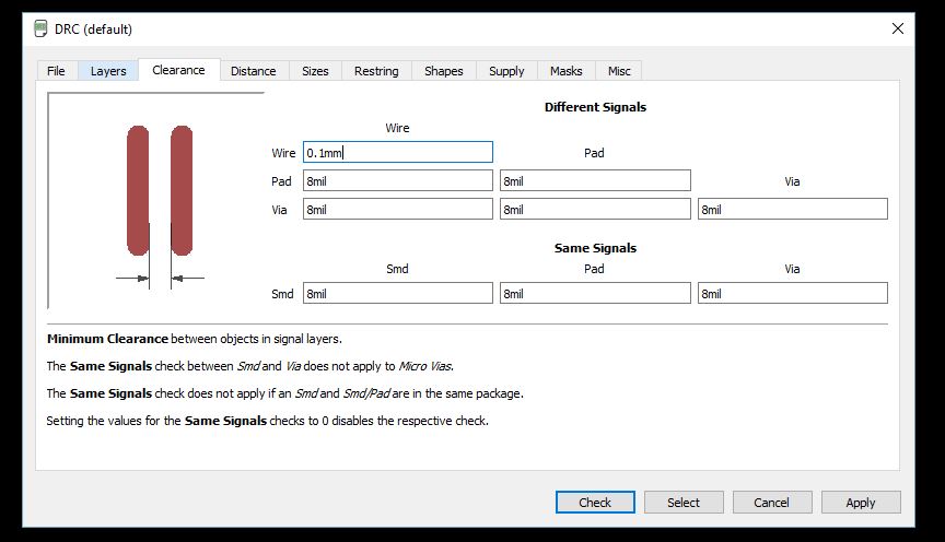
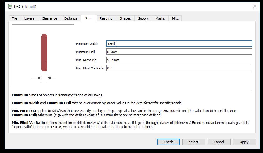
To achieve that the electronic board is manufactured well, it must be secured using the DRC (Design Rules Check), here you can configure some parameters such as the width of the separation between tracks, and the tracks themselves, then I show the parameters that I use .
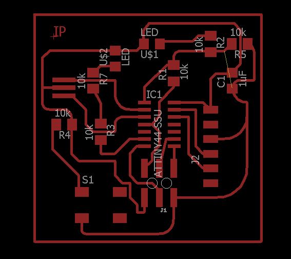
Then I click on the check option of the DRC to see if there is an error with my design that complicates its manufacture, as shown in the image many errors will be found due to how close the pinheader tracks are, for this reason I designed them more separated this time.
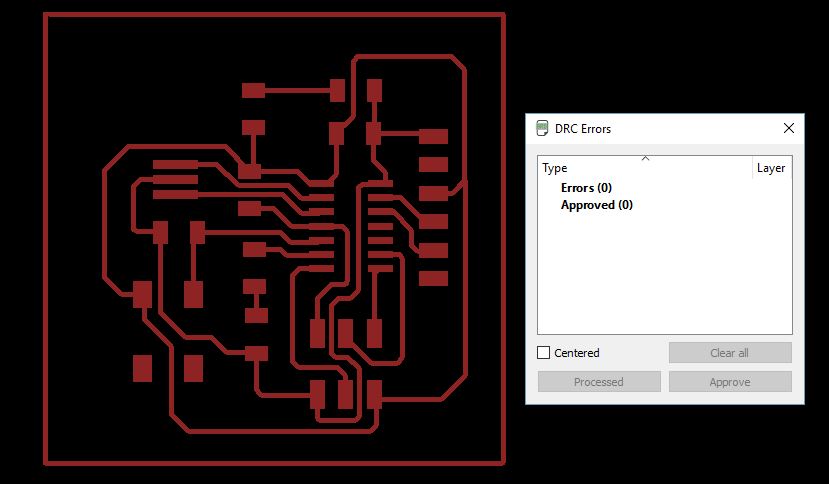
I corrected the tracks and there are no mistakes, respecting the area between traces. I just kept some layers, to see the errors in these, this is the result, apparently had a through hole component, with the same dimensions of the SMD, but with holes
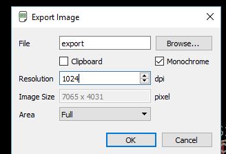
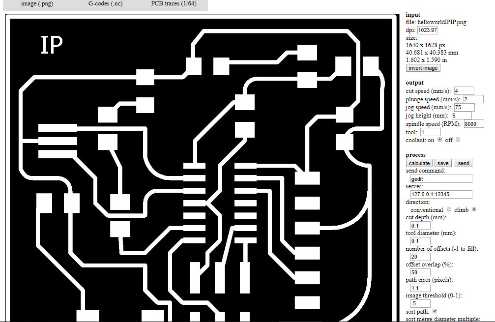
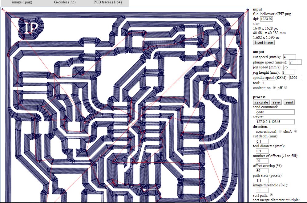
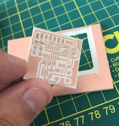
Then i hide the components and show only the traces, i did this to export my design as monochrome PNG with 1024 of resolution, to make the CAM
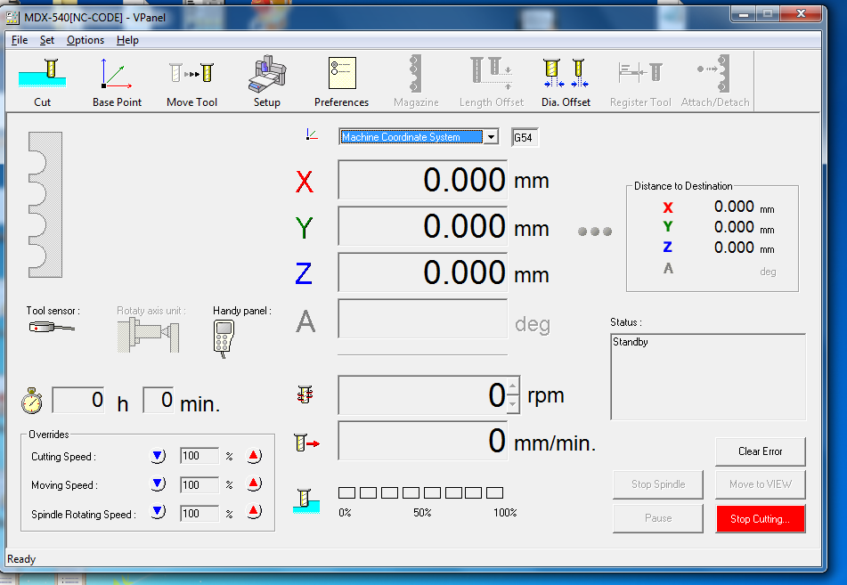
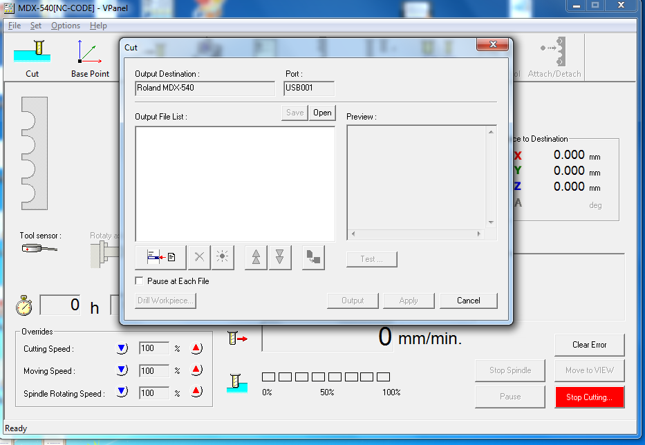
The Roland will machine the black part, removing the copper , i put the following parameters: 8000 rpm, cut depth and diameter tool 0.1 mm
Milling
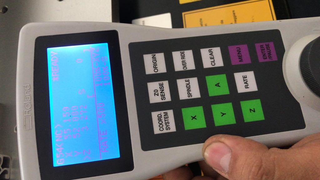
First, i put the board on the plate of the machine and started the calibration
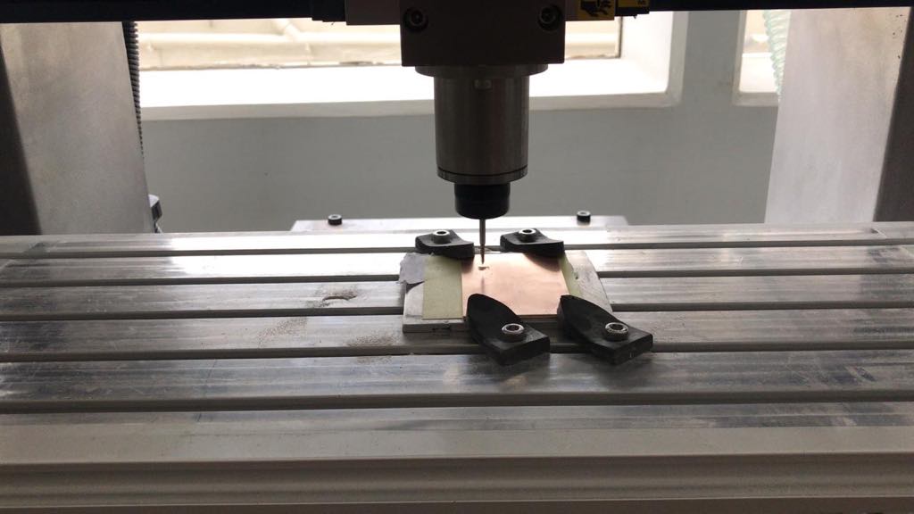
Milling!
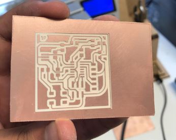
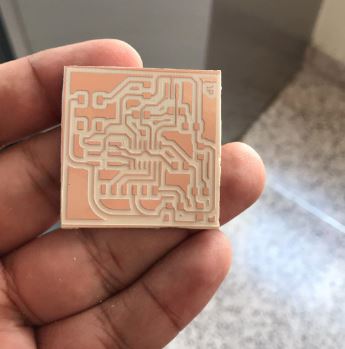
Milling result!
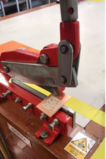
I cut the board with this machine
This is the result
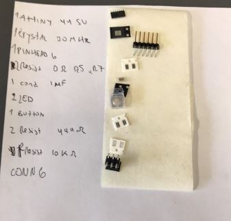
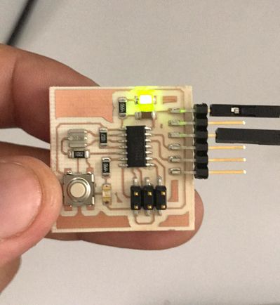
Time to solder
First i identified the electronic components
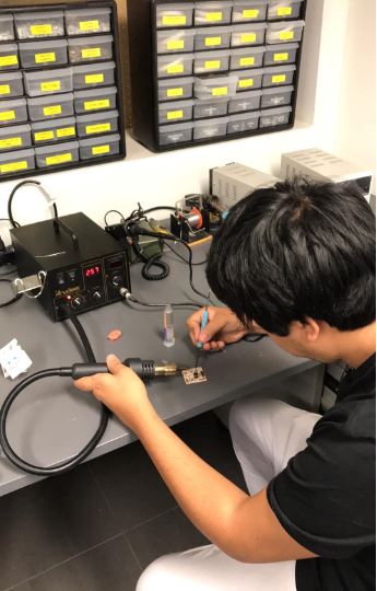
And start to solder
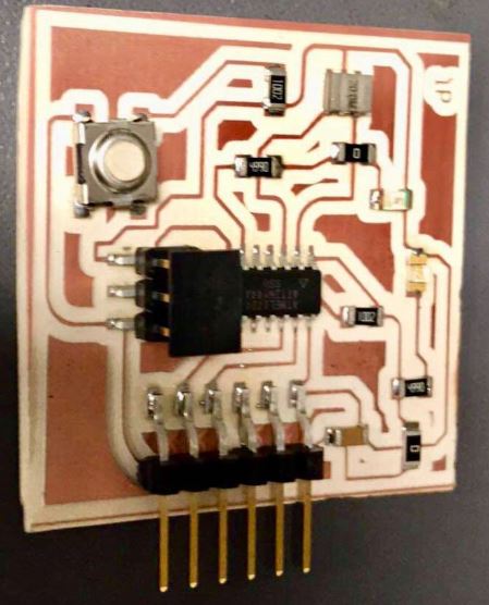
Final result
I forgot to call the label "button" so i had to make the design again
Schematic
PNG
Then I made the machining of the outline traces separately, in a second operation, this is the result
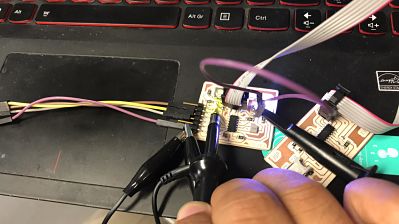
After the solder, i connected my board to vcc and ground, this is the final result!
I uploaded a small code to see if my board worked correctly, the programming is in the corresponding week 9
I uploaded a small code to see if my board worked correctly, the programming is in the corresponding week 9
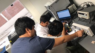
Group Assignment
My partner Edwin designed and soldered the group board, as you can see in his Website.
His design has 2 LEDs as output, so we use an oscilloscope to see the voltage
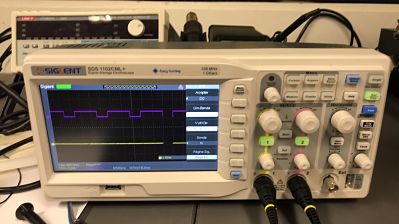
We programmed a blink, when LED1 is ON, LED2 is OFF.
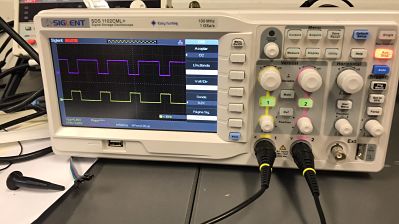
We can see that LED1 has 5V when is activated and LED2 has 2.5V when is in the same situation.
Downloads
Schematic boardPNG board
Board file board