
Electronics Design.
For the assignment of the 7th week: Electronics Design, it will be divided into 4 differentiated parts: Components, Software, Fabrication and a group assignment.
The goal of this week it is create a new electronic board based of the Hello World board.
Components
It is very important to know the importance and the use of the components that we will use for the creation of the hello world board, because it is the bases of the future boards that will be created throughout the academy. For the moment we will see the most important components that will be used this week.Resistors
In order to talk about resistance, the first thing we must know is the electrical resistivity of a material. The electrical resistivity measures the capacity of the material to oppose the flow of electrical charge through them.Depending on the resistivity of the material, they can be divided into conductive, semiconducting and insulating materials. A resistance is a component that varies the intensity of electric current that passes through it. Its unit of measurement is the ohm (Ω).
There are two types of resistances.
- Fixed resistors. It has a fixed value and is standard.
- Variable resistors. The resistance value varies depending on several factors such as temperature, pressure, etc. The most common are the potentiometers.
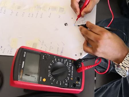
| Stardard value | Real Value |
|---|---|
| 100Ω | 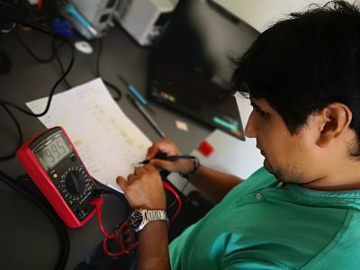 |
| 10KΩ | 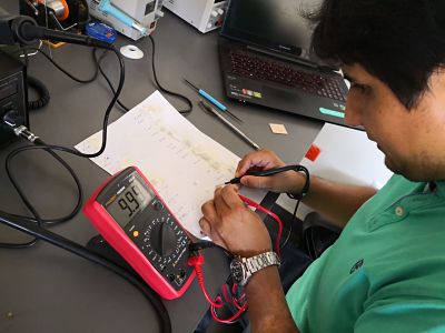 |
| 499Ω |  |
Capacitor
A capacitor is a device that is responsible for storing an electric charge. The most common use given to the capacitors is to filter the electrical current.It is composed of two metal plates that do not touch each other and between which there is a dielectric element (a substance that misses the electricity), which generates a voltage difference between the two plates. The voltage is proportional to the electrical load that the capacitor can be store. This proportionality is measured by a value known as capacitance (C), whose unit is the Faradio.
Some capacitors are polarized, meaning that they have a positive side and a negative side. For this example, we will use a unpolarized capacitor.
Like the resistances, these elements usually have a tolerance, as seen in the picture.
| Stardard value | Real Value |
|---|---|
| 1uF | 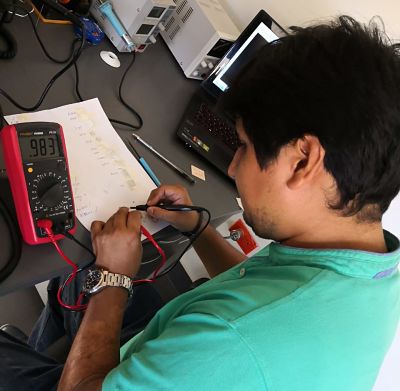 |
Diode
A diode is a semiconductor device that acts essentially as a unidirectional switch for the current. It allows current to flow in one direction but does not allow current to flow in the opposite direction. The diodes have a polarity determined by an anode (positive terminal) and a cathode (negative terminal). Most diodes allow current to flow only when voltage is applied to the positive anode.In the fabacademy we will see three types of diodes:
- Schottky. They are devices that have a very small direct voltage drop (VF). They operate at very high speeds and are used in power sources, high frequency circuits and digital systems. They also receive the name of fast recovery diodes (Fast recovery) or hot carriers.
- Zener. Unlike a conventional diode that blocks any current flow through itself when it is reverse polarized, as soon as the reverse voltage reaches a predetermined value, the Zener diode starts to drive in the reverse direction. This is the most prominent feature of this element.
- Led. A Led diode is a diode that, in addition to allowing the passage of the current only one way, in the direction in which the current passes through the diode, it emits light.
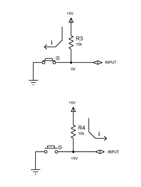
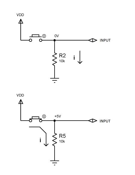
Button.
A button is a device that allows the passage of electrical current when it is held down. There are two configurations:- Pull-up. When the pushbutton is pressed, the current circulates through the resistance and then through the pushbutton, in this way we have that the voltage at the input is Earth or 0V. I use this configuration.
- Pull-down. In the pull-down configuration when the button is at rest, the input is 0 and when pressed, it will read 1 or 5V.
Crystal and Resonator.
Crystal
The crystal oscillator is an electronic component capable of generating an electric current with a very precise frequency, this frequency is used as a clock on our electronics board with a microcontroller. When we subject the crystal oscillator to a certain voltage, the material of the oscillator produces a current with a certain and precise frequency. These are usually accompanied by two capacitors that act as a signal filter.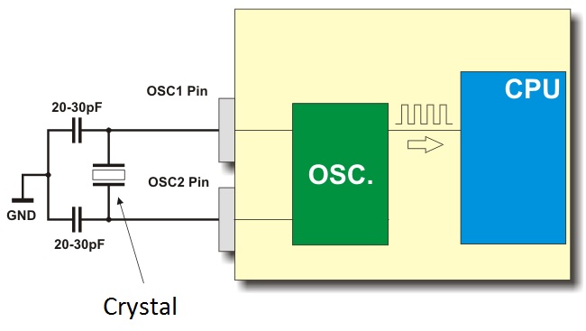
Resonator
A resonator is a component composed of a crystal oscillator and two capacitors in the same encapsulation, as shown in the picture.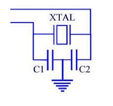
Microcontroller
The Microcontroller is an integrated circuit that is the main component of an embedded application. It is like a small computer that includes systems to control input / output elements. It also includes a processor and of course memory that can store the program and its variables (flash and RAM). It works like a mini PC. Its function is to automate processes and process information. The microcontroller is applied in all kinds of inventions and products where it is required to follow an automatic process depending on the conditions of different inputs.Attiny44
The high-performance, low-power Microchip AVR RISC-based CMOS 8-bit microcontroller combines 4KB ISP flash memory, 256-Byte EEPROM, 256B SRAM, 12 general purpose I/O lines, 32 general purpose working registers, an 8-bit timer/counter with two PWM channels, a 16-bit timer/counter with two PWM channels, internal and external interrupts, an 8-channel 10-bit A/D converter, a programmable gain stage (1x, 20x) for 12 differential ADC channel pairs, programmable watchdog timer with internal oscillator, a internal calibrated oscillator, and three software selectable power saving modes. By executing powerful instructions in a single clock cycle, the device achieves throughputs approaching 1 MIPS per MHz, balancing power consumption and processing speed. More information here.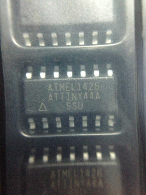
Software
Among the diversity of existing softwares for the creation of PCB, I have decided to use the software: Autodesk Eagle for windows. I have been using this software for several years. In week 5 I refer to the use of the software.Eagle
This software is specialized for the creation of electronic circuits for its later manufacture. This software does not specialize in the simulation of its fining, only in the creation. If you want to simulate you can use other software such asfritzing or KiCad.
Library
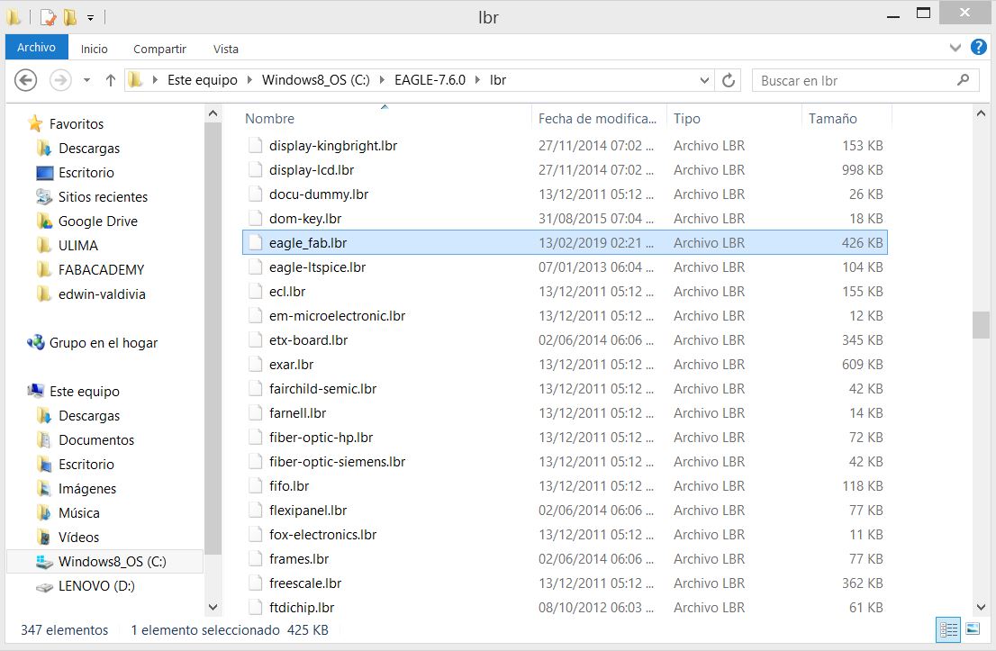
To avoid errors when manufacturing our design, we must use the correct library with the components that we have in the laboratory with their exact measurements. Therefore, the first thing we must do is download the eagle_fab libraryOnce downloaded, we must paste it into the library folder where we have installed our eagle, as shown in the picture.
Fabrication
With the software and the library installed, we proceed to make the new design of the board using the fab academy tutorial as a reference.Schematic and board
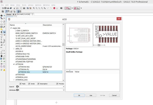
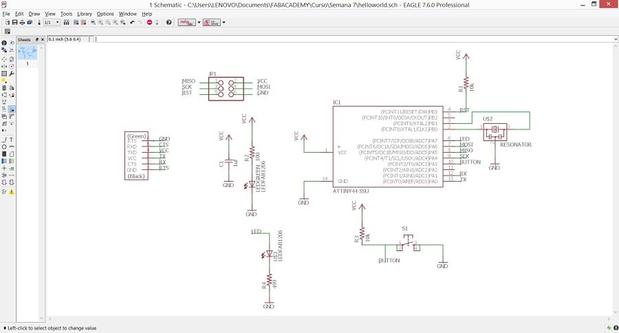
A schematic in electronics is a drawing representing a circuit. It uses symbols to represent real-world electronic components. The most basic symbol is a simple conductor (traces), shown simply as a line. If wires connect in a diagram, they are shown with a dot at the intersection.To start making the new design, you must add the necessary components, the process of adding the components are seen in the picture.
 The list of the components of echo hello world are the following:
- 6-pin programming header.
- Microcontroller attiny44A.
- FTDI header.
- 20MHz resonator.
- Capacitor 1uF.
- Resistor 10KΩ.
- White Led.
- Blue Led.
- Button.
- Resistor 100Ω.
- Resistor 499Ω.
- Resistor 10KΩ.
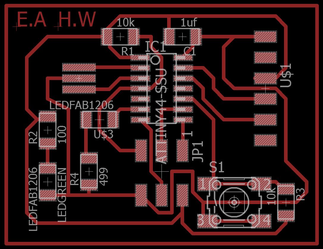
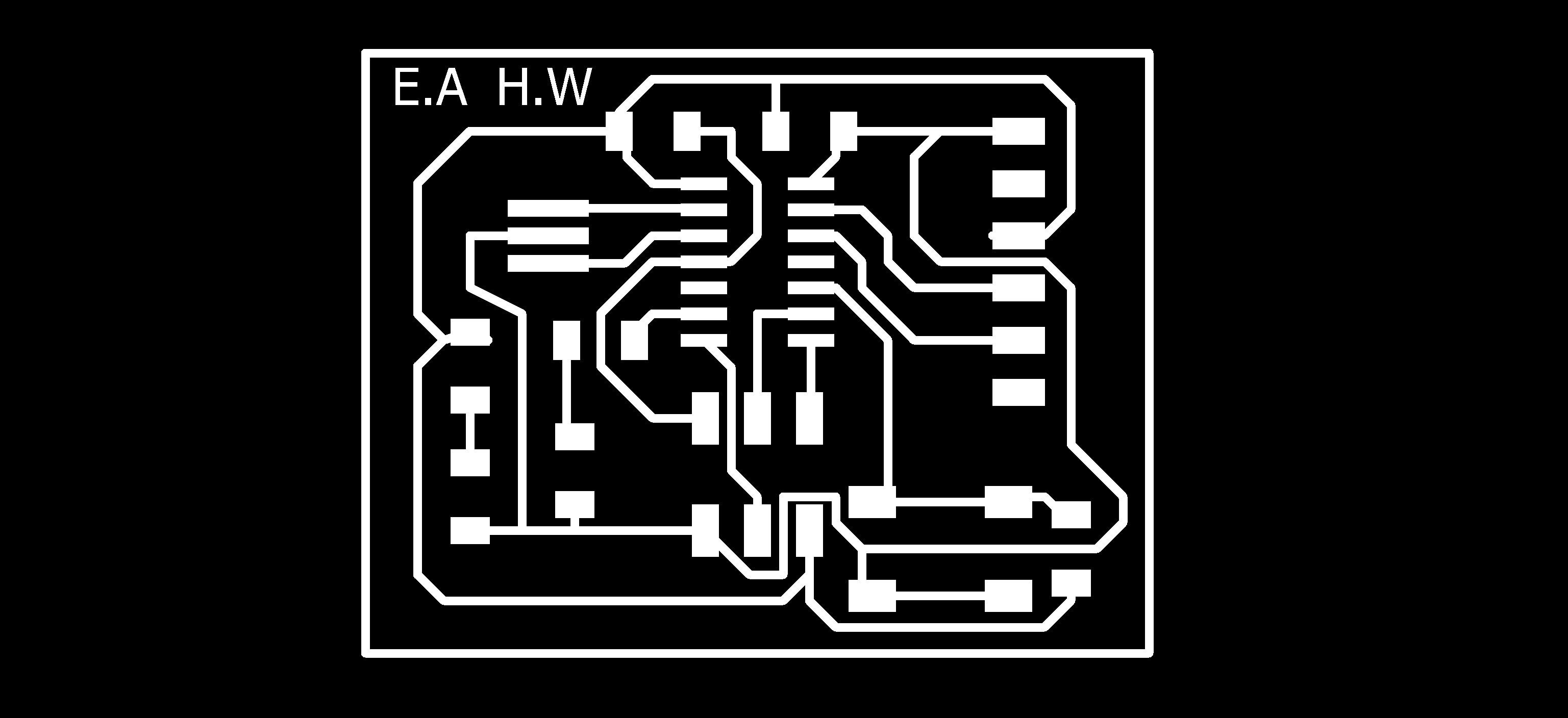
 Once the schematic is finished, we have to carry out the board, where we will define the routes of the conductor tracks and the location of the components, for this we click on file-switch to board.
Based on this tutorial, we made our design that has this final design.
Once the schematic is finished, we have to carry out the board, where we will define the routes of the conductor tracks and the location of the components, for this we click on file-switch to board.
Based on this tutorial, we made our design that has this final design.
 To avoid failures at the time of manufacturing, you must use the DRC (design rules check). From here we can configure parameters of cutting distance, diameter of the milling cutter, etc.
When using the DRC, the parameters are configured as shown in the picture.
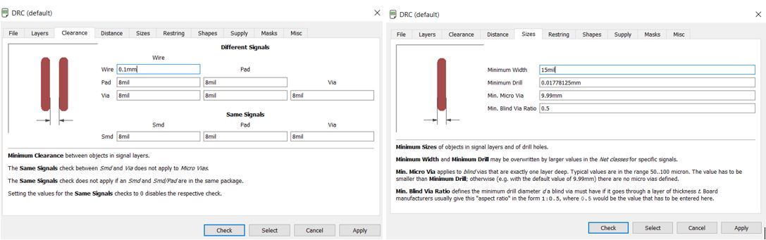 These parameters are defined according to the tool that is used in the Roland.
Once the parameters are configured, click on check and check the errors.
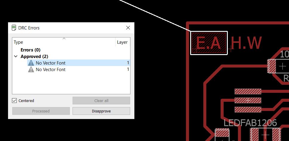
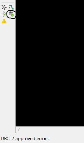 The errors that are appreciated only affects the size of the letter, it is not directly to a serious error of the design, that's why I approve it manually.
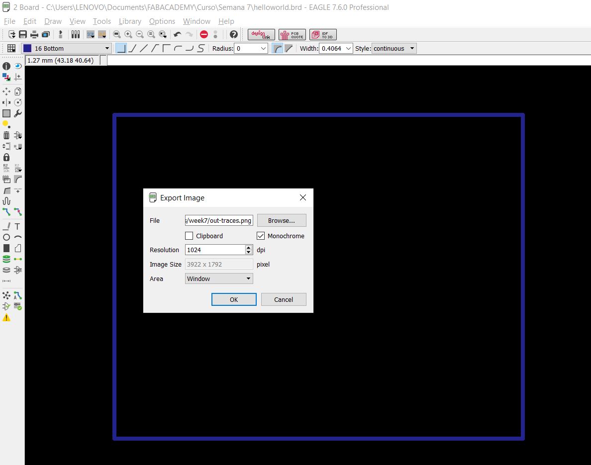
 Before exporting our design to an image format, we must cancel the unnecessary layers, we just have to keep the layers we see in the picture:
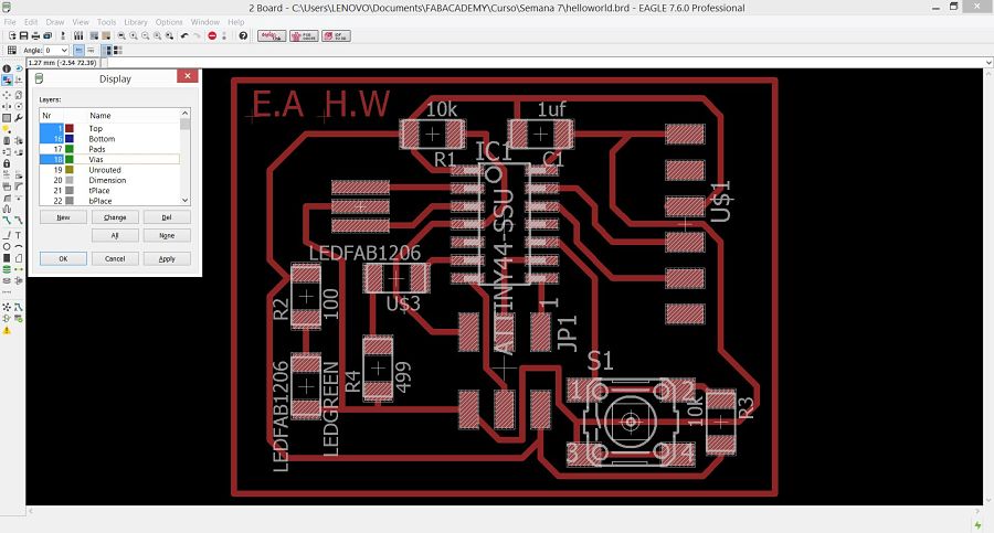 By activating only the necessary layers, we have the following result.
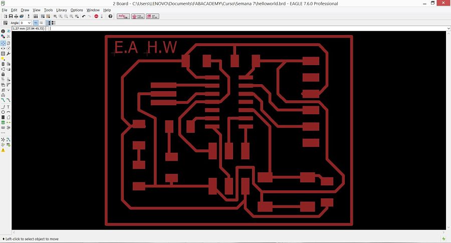 In the bottom layer I draw an outer rectangle with the wire tool, as shown in the figure.
This external square is created to obtain the out traces, this is necessary to be able to cut the plate to a reduced size as we will see later.
In the bottom layer I draw an outer rectangle with the wire tool, as shown in the figure.
This external square is created to obtain the out traces, this is necessary to be able to cut the plate to a reduced size as we will see later.
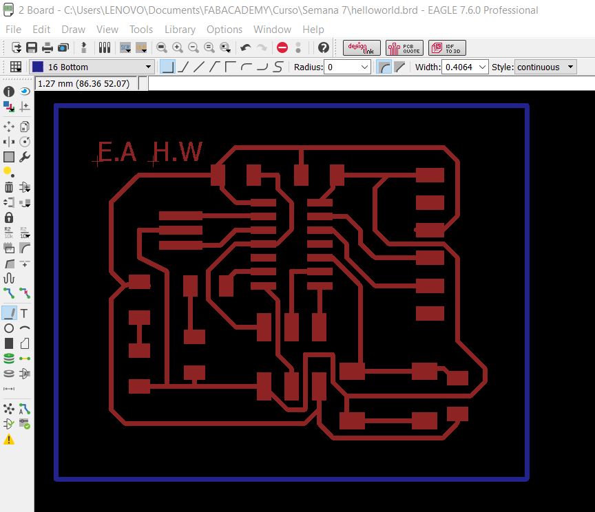 We carry out the same steps to export the image of the exterior for its later cutting, only that in this opportunity we activate only the bottom layer
Machining
Proceed to perform the same steps that can be seen in week 5 (click here), the plate is cut using the first fabmodules of the helloworld board with the same parameters as the ISP, as shown in the picture.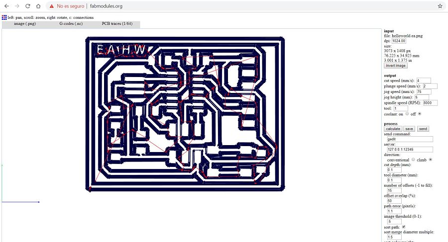
Below is the result of machining.
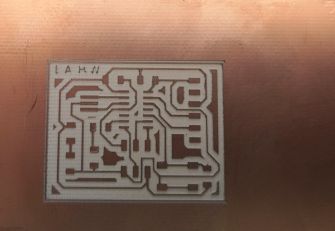
We can appreciate that a correct in the manufacture of the board was made. In addition, a test of a linear cut was carried out manually to check if they really are the correct measurements.
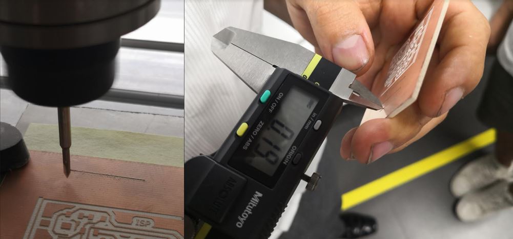
At a 0.1mm depth cut, the width of the line is 0.19mm, the theoretical measure being 0.1mm. With this result we must be careful not to overlap the circuit lines to avoid continuity cuts.
After cutting the traces, an exterior contour with a depth of 1.55mm is cut. For the out traces other parameters are used that are detailed below:
| Cut Speed | 2 mm/s |
| Plunge speed | 1 mm/s |
| Jog speed | 40 mm/s |
| Spindle speed | 10000 RPM |
| Cut depth | 1.55 mm |
| Tool diameter | 1 mm |
| Number of offsets | 1 |
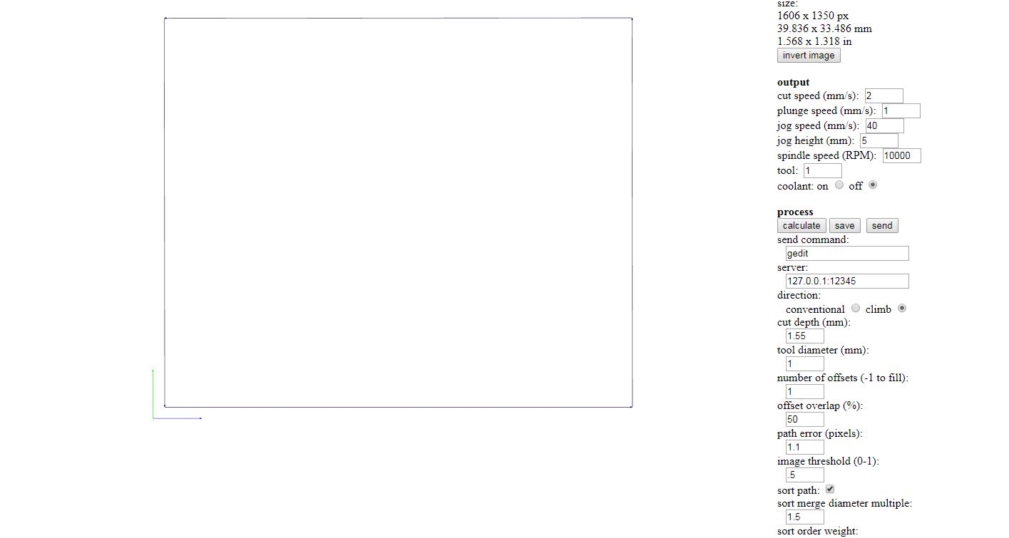 In order not to break the board, 4 similar cuts will be made, the first at 0.1mm depth, then the others increasing to 0.5, 1.0 and 1.5mm, in total 4 similar jobs are performed.
Soldering
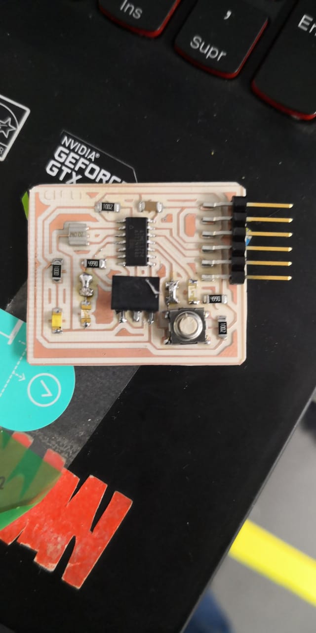
Finally, we started to carry out the soldering operation, having identified all the necessary materials until obtaining the final board.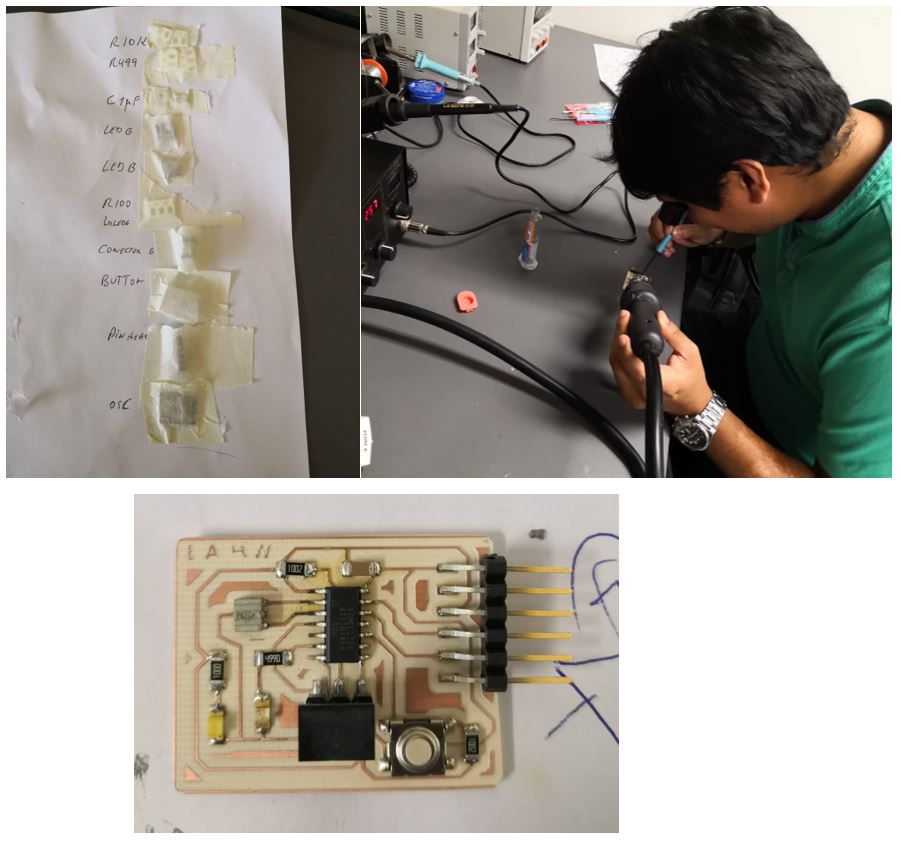
First test
The only way to test this board without programing, is connecting 5V to vcc and test the leds, like the picture.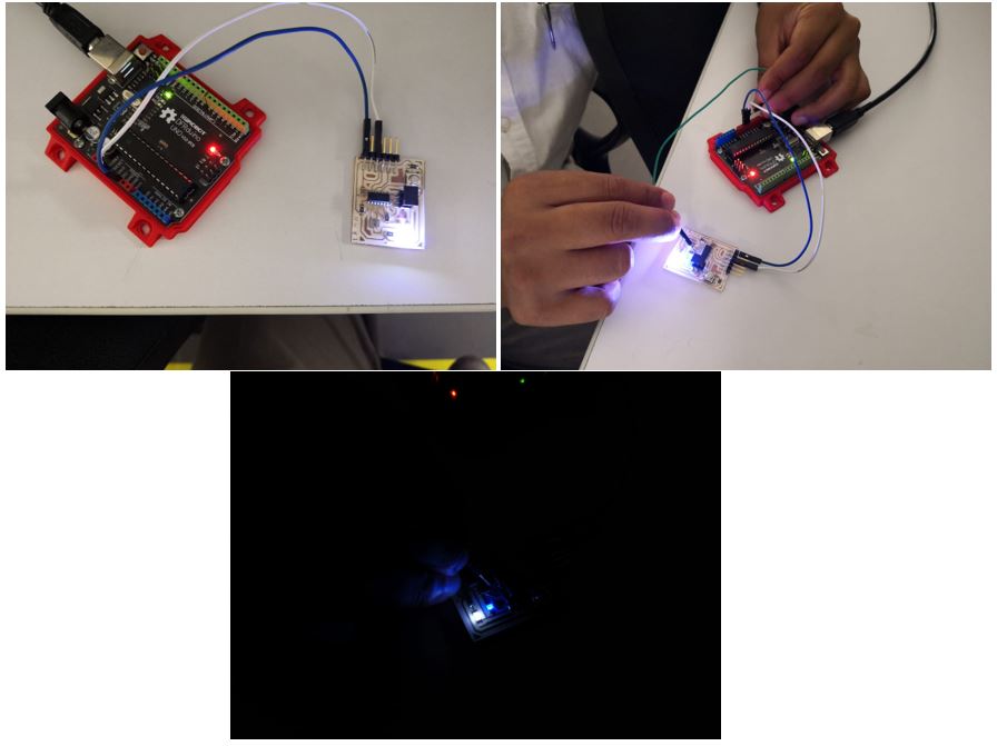
Second test
Using the following tutorial, I went ahead in making the programming of the board, getting its operation that can be seen in the following video.Group assignment
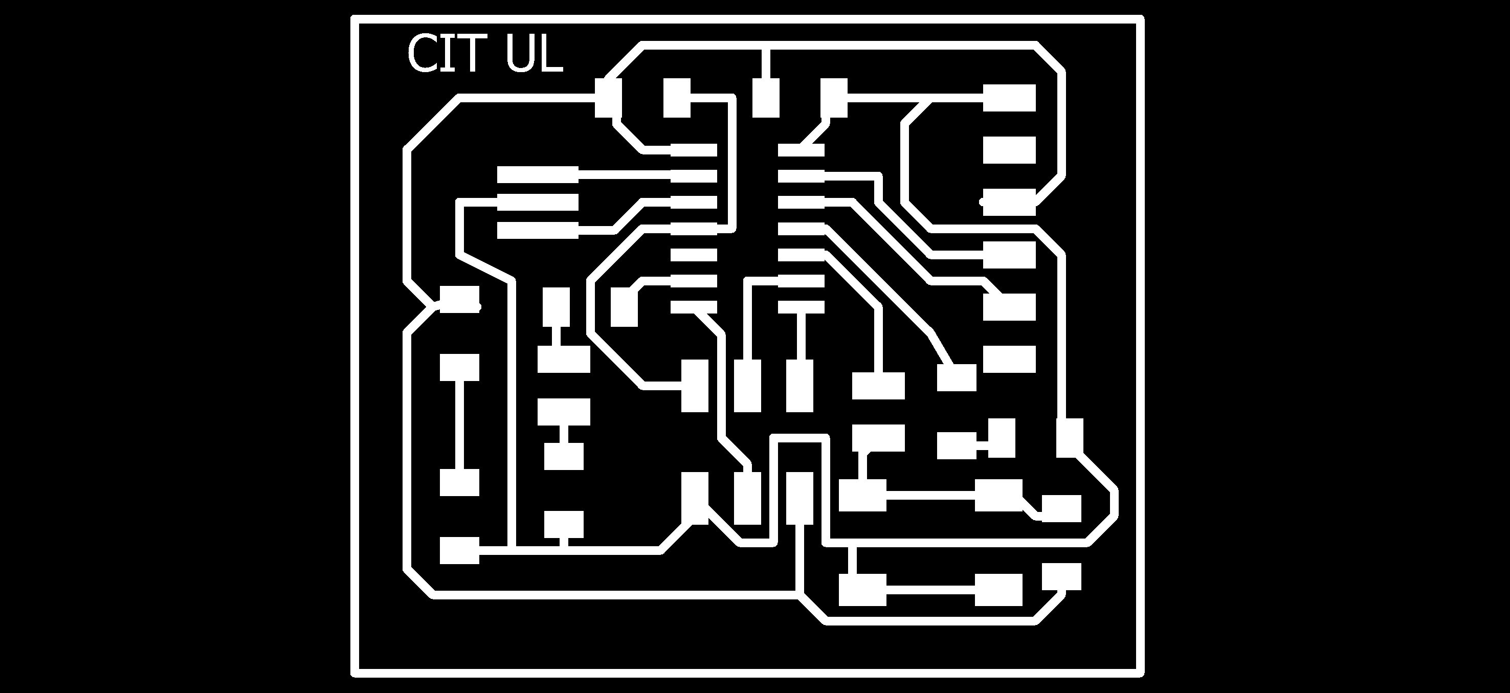
For group work, my contribution was the creation of the plate, in which I basically add an additional led to my design, in addition to using a welding jumper on a led and the button, to know the current consumption and use the oscilloscope.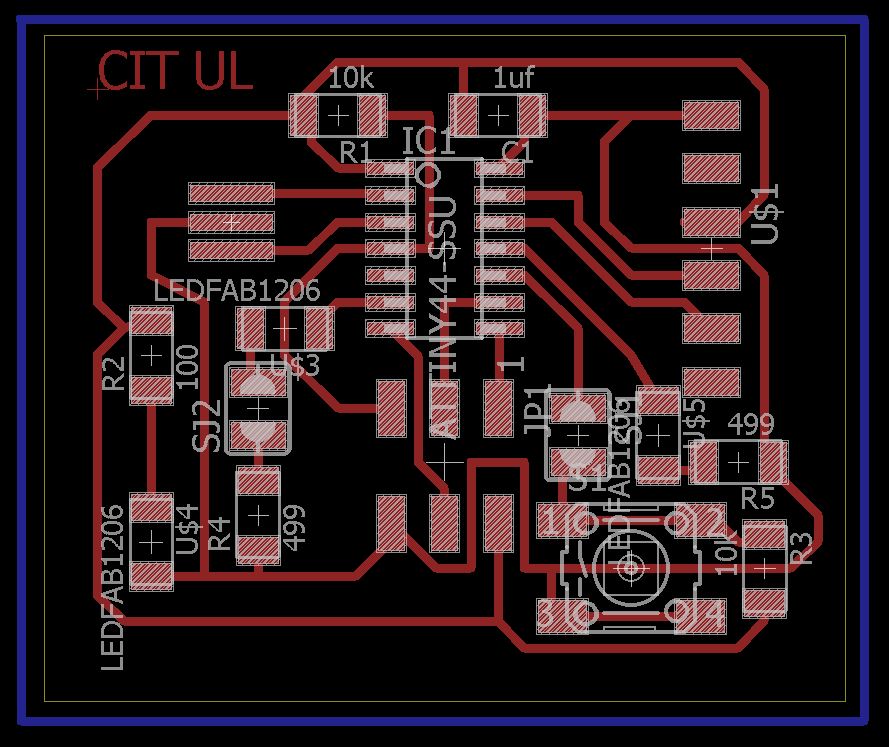 After fabrication and soldering, the final board is the one shown in the picture:
Test
The first test that is carried out is to know the intensity of current that circulates through the Led of pin 6 of the Attany, resulting in a consumption of 4mA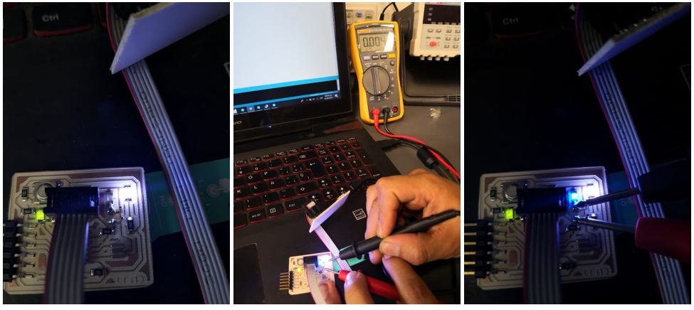 A second test that is carried out is the power on of the led with the oscilloscope. On the board there is a led on pin6 and another one on pin11.
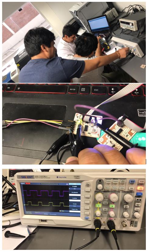 We can see how one LED is activated and the other is not, depending on the programming, with one LED having a voltage of 5V while the other one has a voltage of 2.5V. The attany's data sheet must be checked to verify the correct voltage.
To see all the documentation of the group work, you can visit the CIT page.
Download files
You can download this files Here:Hello World board
Hello World schematic
PNG board
PNG out traces
Group files.
PNG Cit board
PNG Cit out traces