

13/2/2019
Characterize the design rules for your PCB production process
Make an in-circuit programmer by milling the PCB, program it, then optionally try other PCB processes
In order to characterize the design rules for our PCB production process, we have to do the line test (see below image). This test enables us to check the range of the line thickness that our milling machine can drill with a specific drilling bit tool
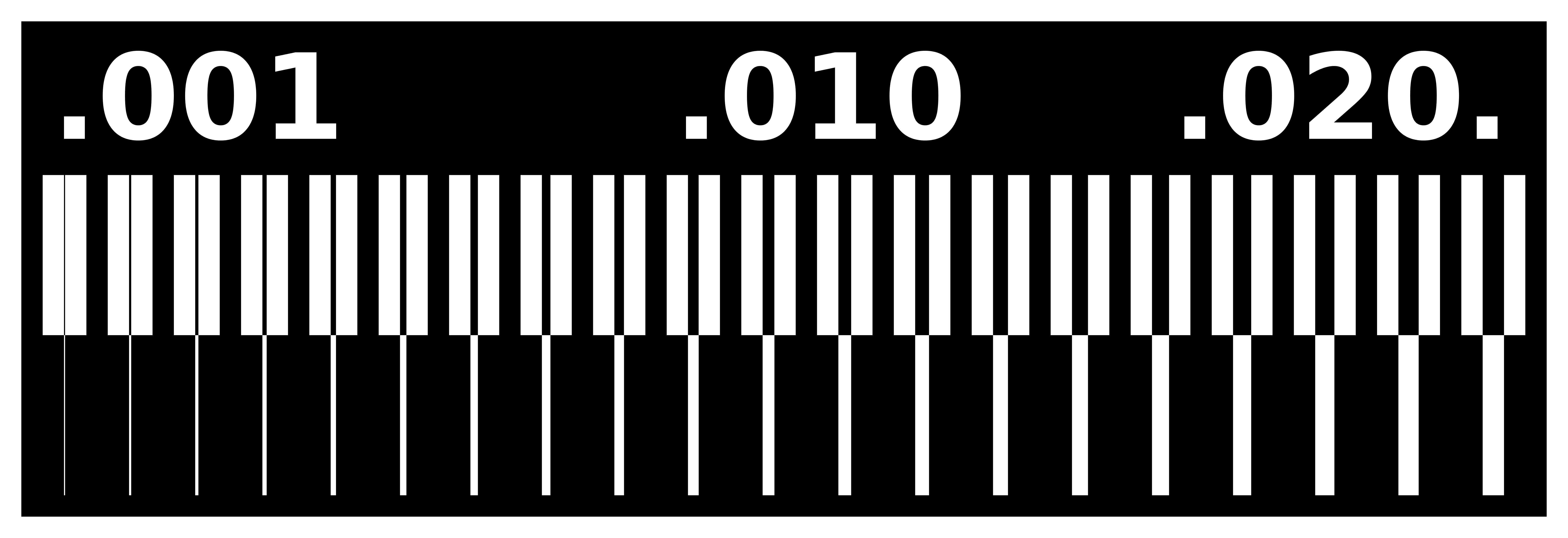
You need to know that the drilling bit cuts or engraves around the white line. All what is in black stays as it is. This means that we need to have two images to be printed; one for the internal path (which is what needs to be engraved inside our frame) and another one for the external path (which is the outer frame that needs to be cut). And for that we need to use GIMP (which you may download from here ) in order to generate the two images
P.S. Make sure that you export your images as PNG
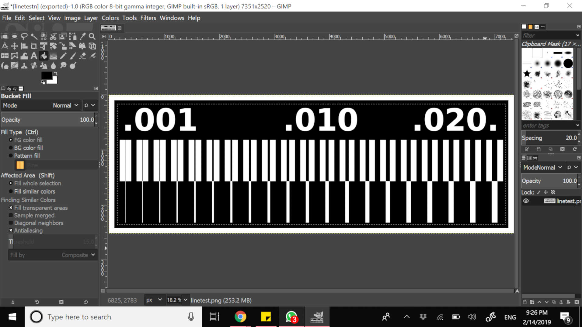
For the image of the internal path, you need to fill the outer border with black paint (from the bucket fill paint tools)
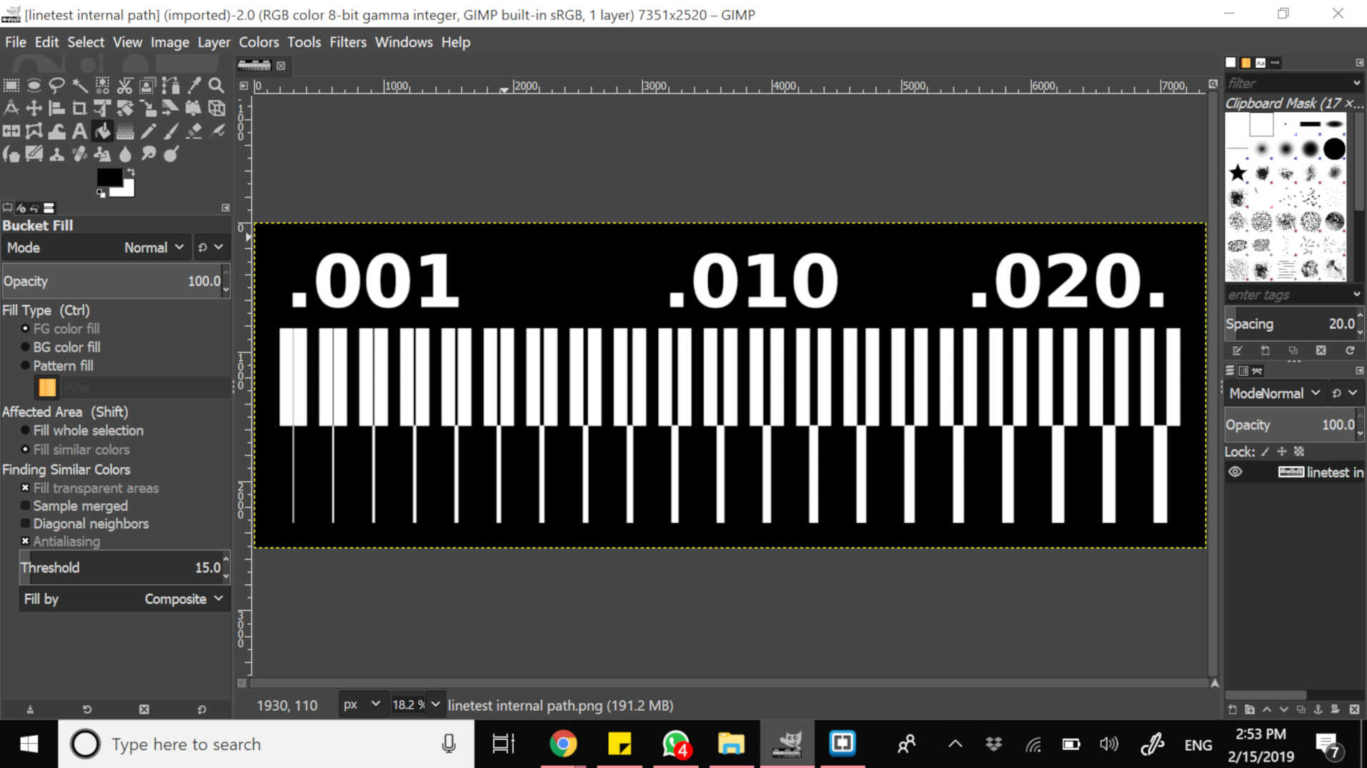
So you may have your PNG of the internal path
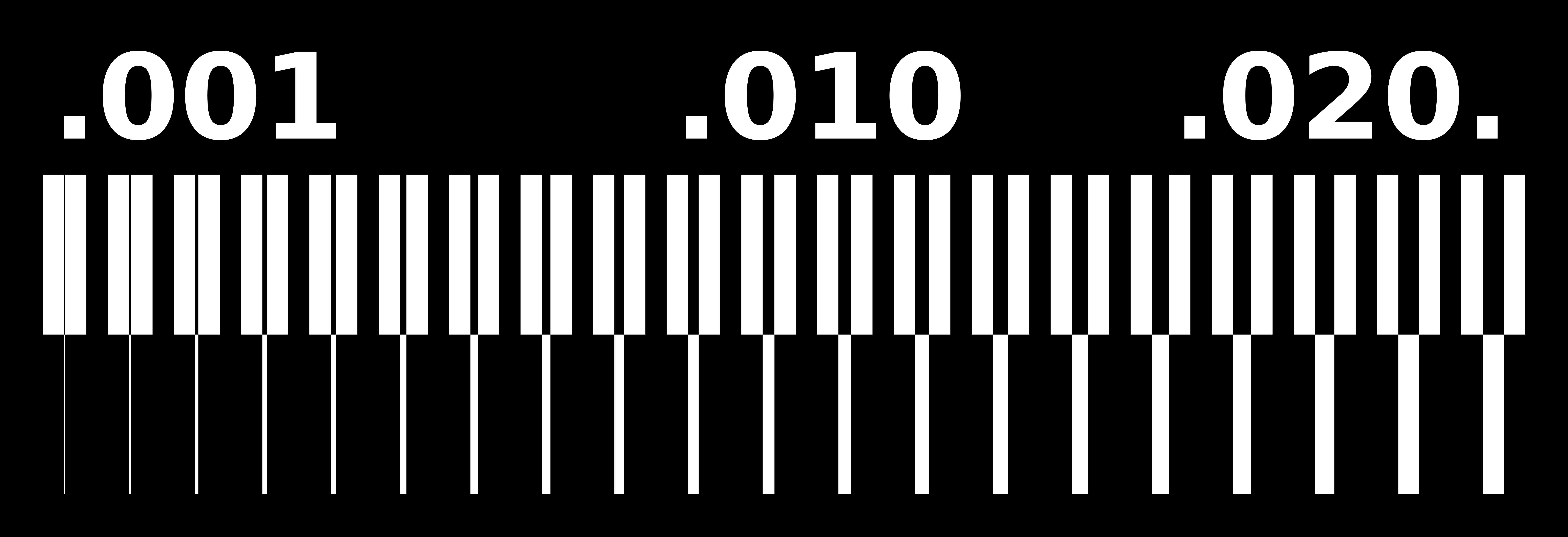
For the image of the external path, you will to draw a selection rectangle all around the white lines and use the bucket fill from the paint tools to paint it in black

Now you have the below image of the external path or outer border of your test

But you need to invert it because the drill bit cuts around the white line. You can do so later
Now you need to generate something called the G code. The drilling machine cannot understand those photos. It needs a G code in order to work. This code can be generated from Fab modules
In fab modules, you need to go step by step. Note that the settings vary between the image of the internal path and the one of the external path
Let's start with the settings of the internal path
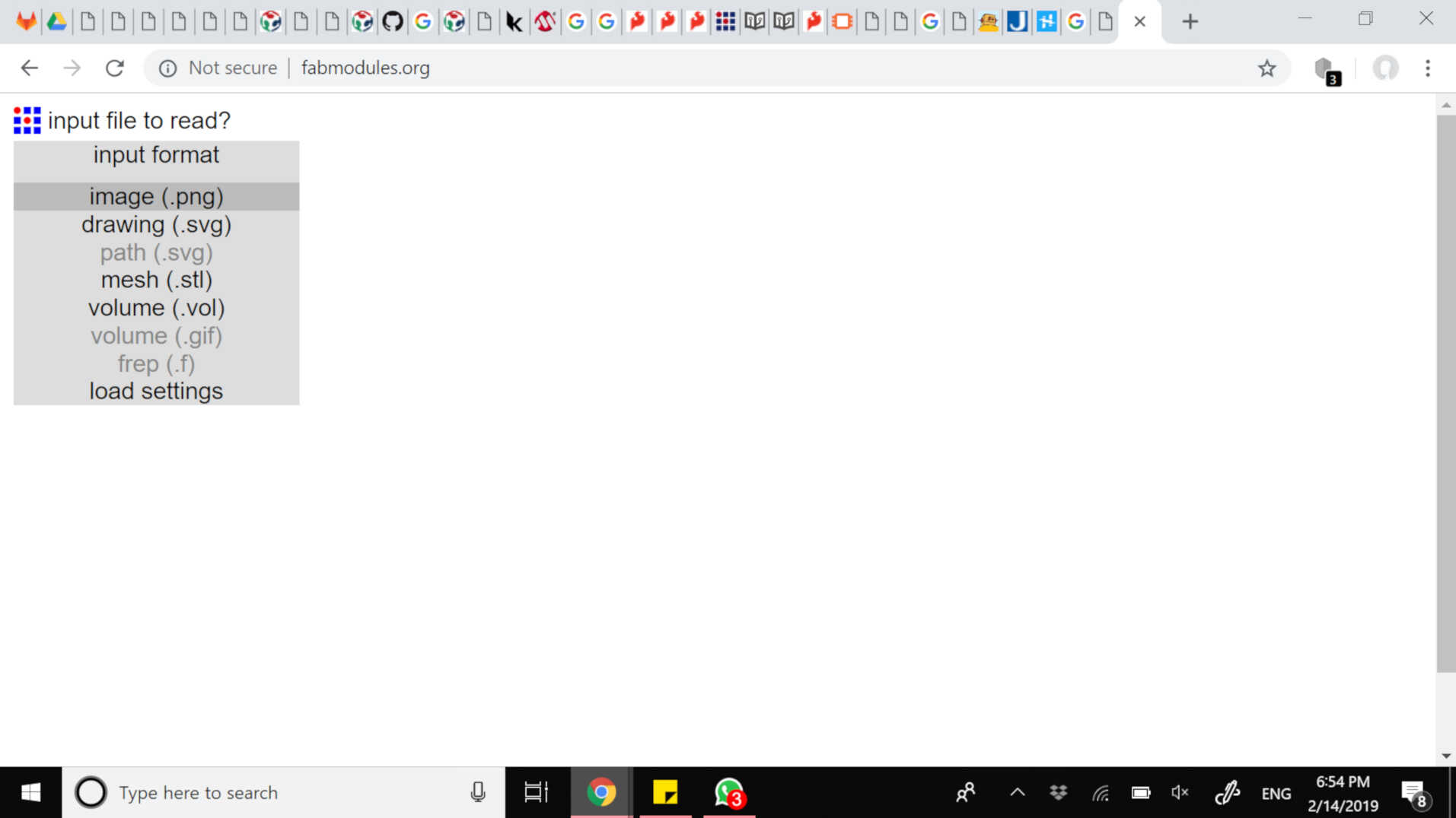
First, import your image
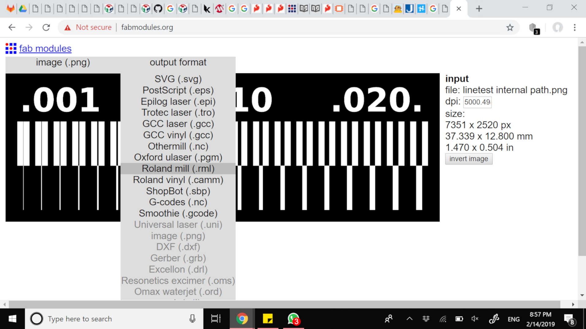
Then choose your milling machine
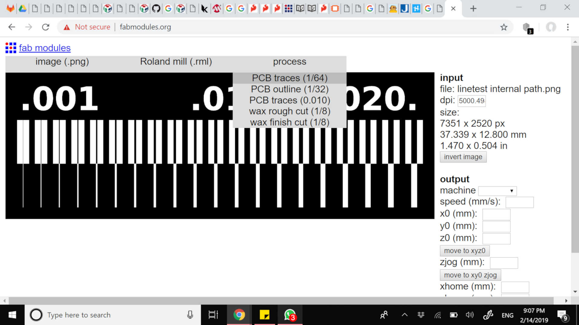
For the internal path or traces, choose PCB traces (1/64)
Then you may complete filling the rest of the settings. You need to select your machine and which is the MDX-40 in our case. Then your speed needs to be 4 mm/s. Your X and Y are always 0. Your cut depth is 0.1 mm, tool diameter is 0.15 mm in our case and the number of offsets is 4 (enough). As for the offset overlap, you may choose 60 or 70%

You may then click on CALCULATE (under process) and wait until you have the below image of your G code
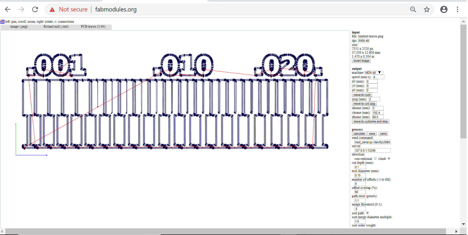
And finally you click SAVE (next to calculate) so that your file is saved as .rml -and which is the format that your drilling machine
You will then repeat the same steps for the external path but you need to apply some changes. First, invert your image. In this case you need to choose PCB outline (1/32), speed of 0.5 mm, cut depth of 1.7 mm, tool diameter of 1 mm, and the number of offsets is 1. The remaining settings are like the ones for the internal path. Do not change any of the rest! And then you calculate and save
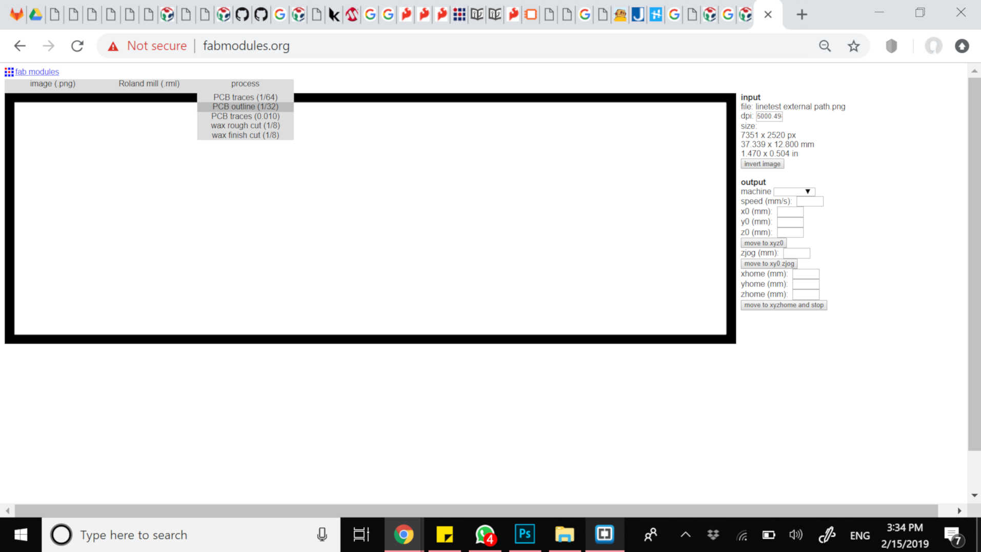

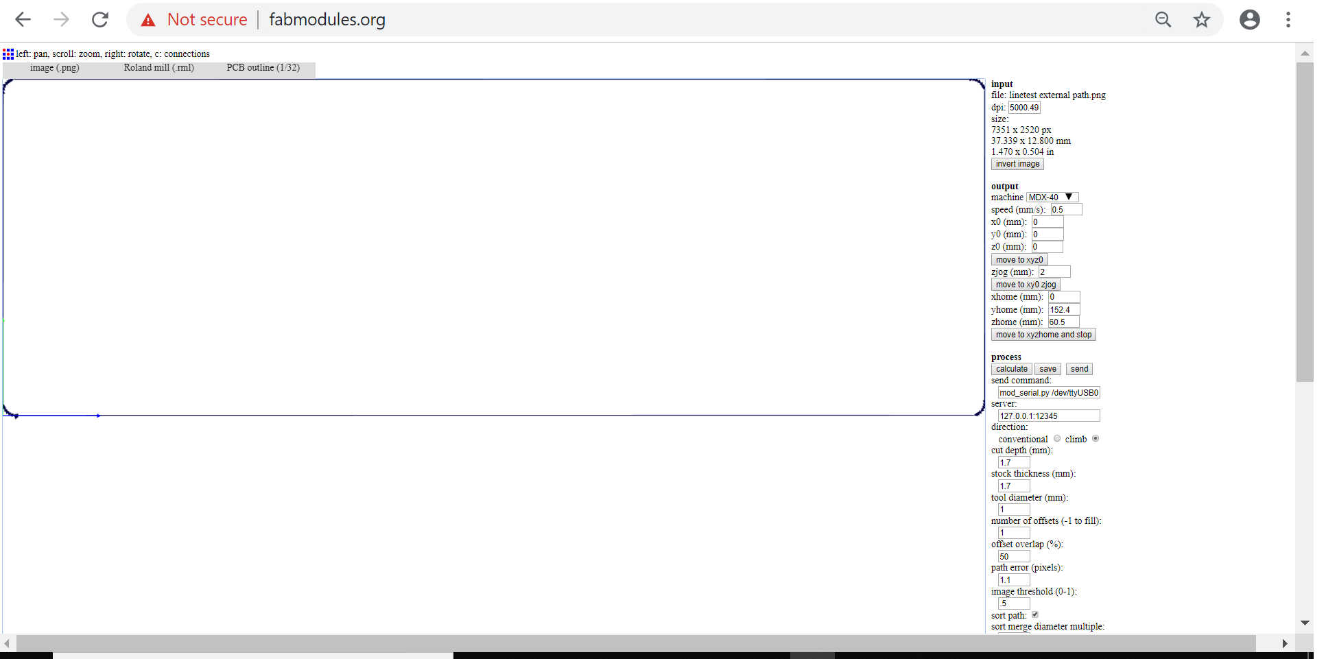
If we want to analyze the above in terms of the relation of the settings we have filled to the drilling machine, we understand that we would need to change our drilling bits (0.15 mm for internal path and 1 mm for external path)
Now, how would we print this file? We need to place our copper board on the bed of the machine and put the corresponding drilling bit of 0.15 mm and close the machine
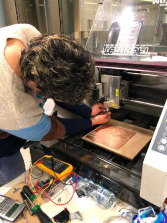
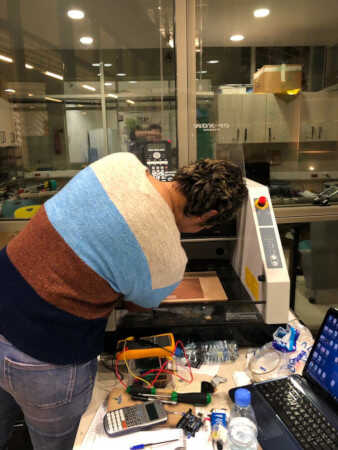
Then we need to open DropOut software on the desktop connected to the machine
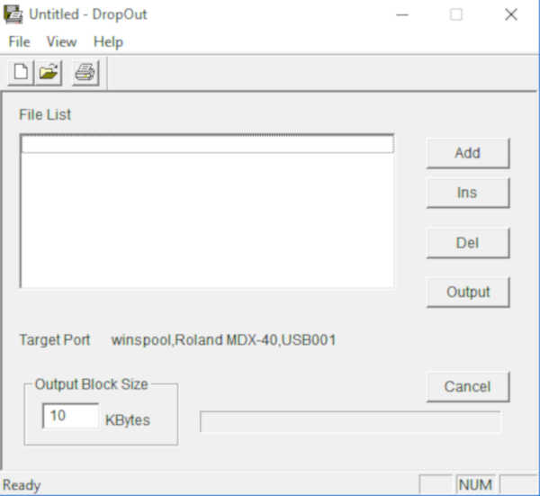
Then add our first file of the internal path which we have saved from fab modules

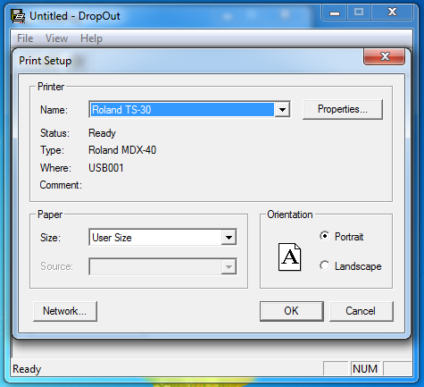
Choose the machine

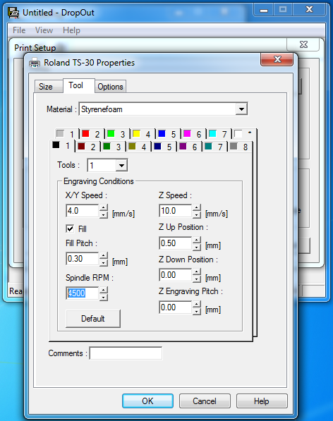
Spindle RPM should be 4500 or 5000 for the internal path
Then we need to position our milling bit
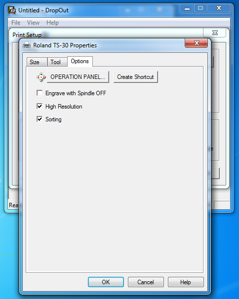
We need to 0 the X and Y axis and set them. Then we set our Z axis. For the Z axis, it is a bit more complicated as the drilling bit (0.15 or 0.2 mm) is very fragile, it shouldn't be touching the board much; it should be pretty close to it without the chance to be broken. So you may connect your drilling bit and your copper board to a multimeter and keep moving your Z axis down until you hear the beep. Then you set it and you are good to press OUTPUT in order to print your file

You will need to repeat the same steps for the file of the external path, after changing your drilling bit to 1 mm (or 1.2 mm). Do not change your X and Y axis. You just need to reset your Z axis. You do not need to use the multimeter in this case. You may just place a paper under your drilling bit and keep pushing the Z axis down until the paper is not coming out very easily from under the drilling bit
Spindle RPM should be 10000 for the external path and you change the below
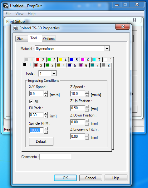
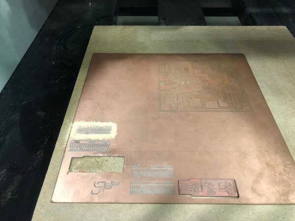

The results of the linetest were unfortunately not satisfying.
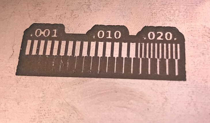
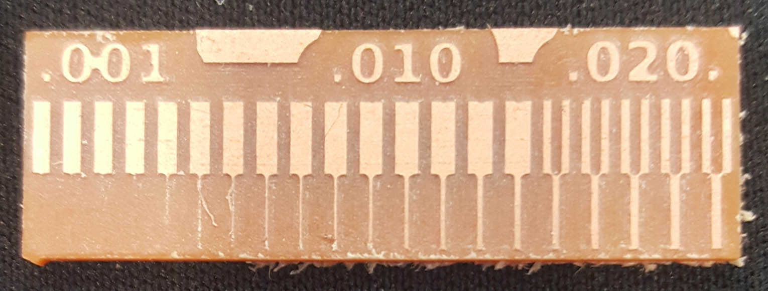
During week 7 of the electronics design, we have repeated the test and used a new milling tool of 0.4 mm instead of 0.15 mm; The results were quite satisfying as per the below!
Time to mill the FabISP
The same steps need to be undertaken as per the above group assignment. And for more instructions or details, you may refer to Brian's page
Below are the ISP internal and external path
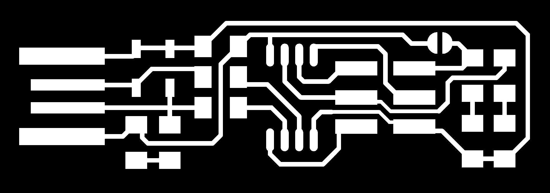

Then you generate the G code of both images
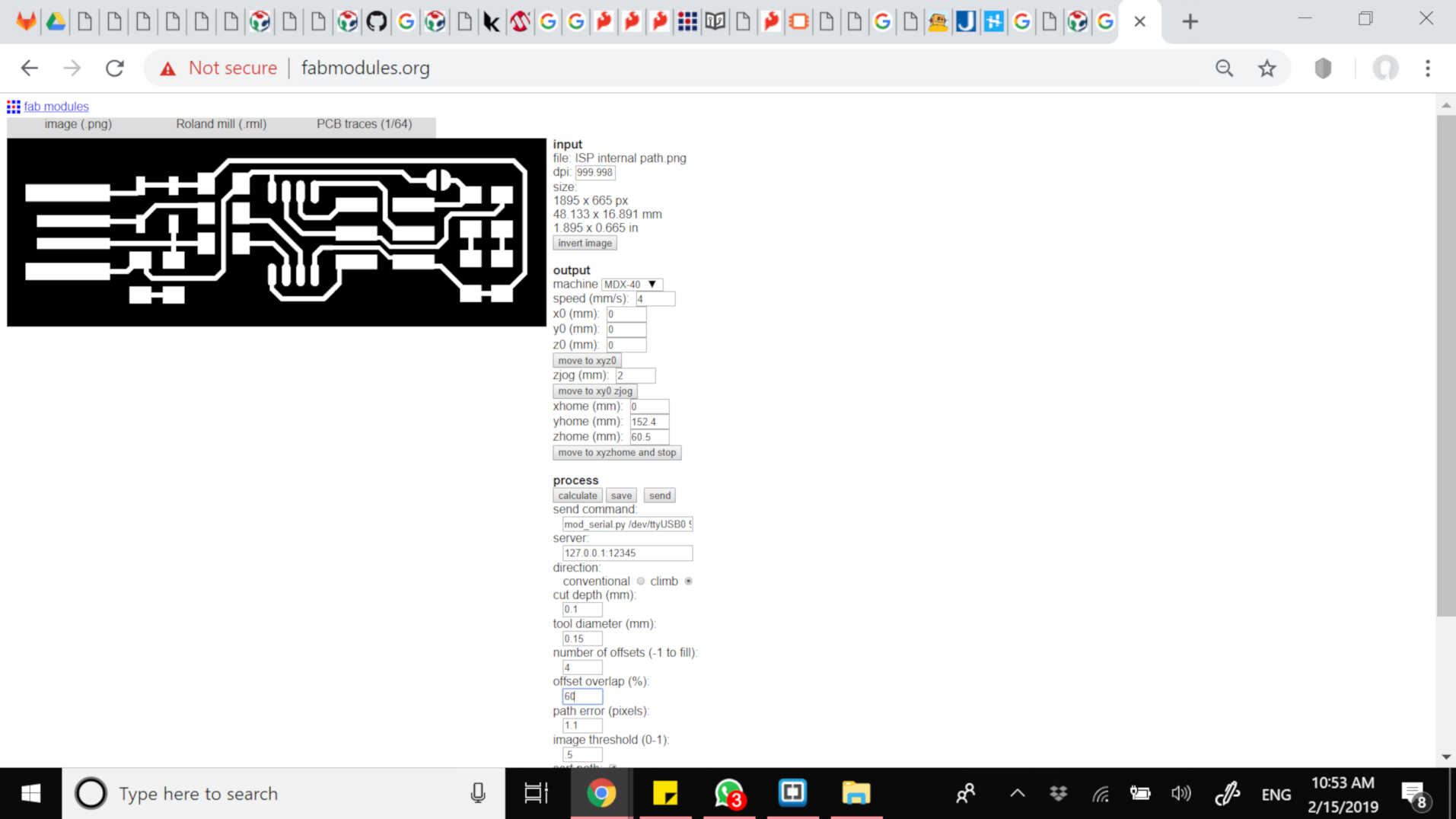
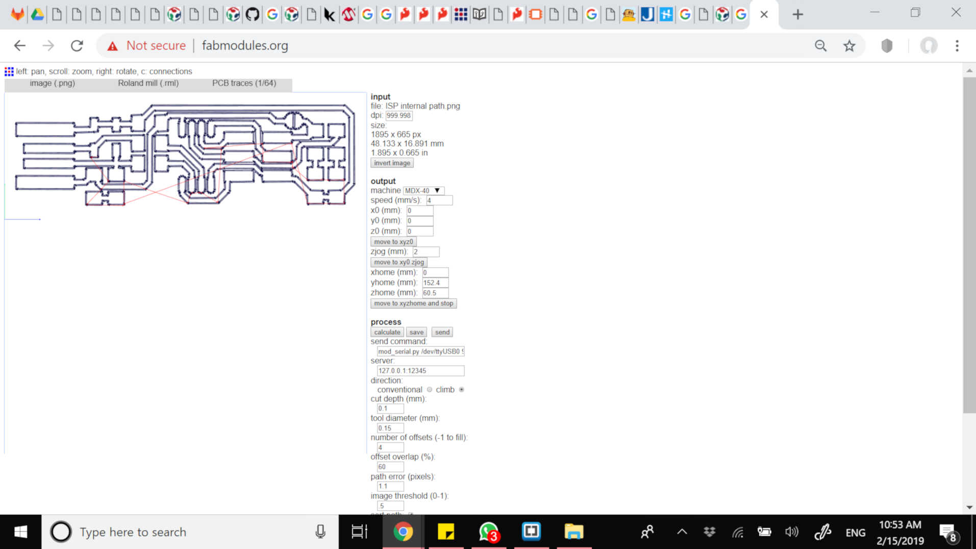
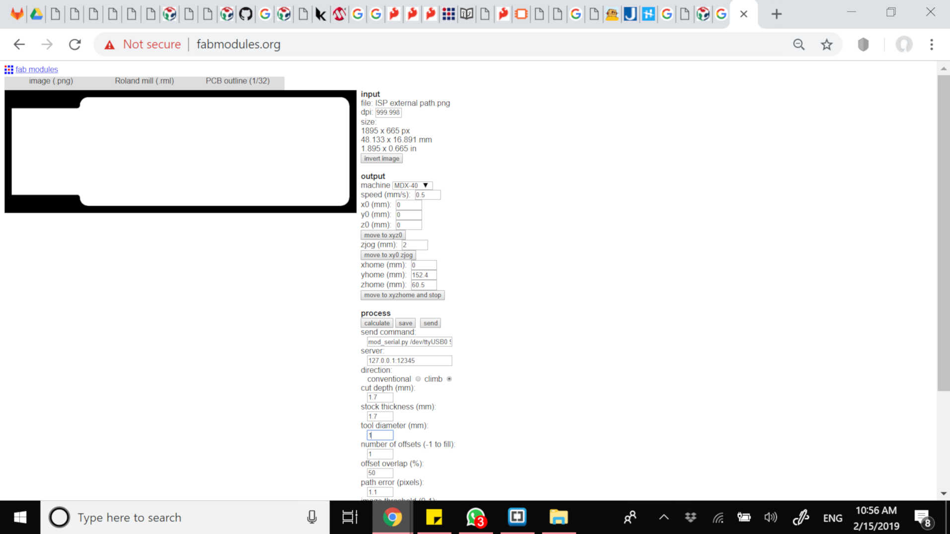

And you mill
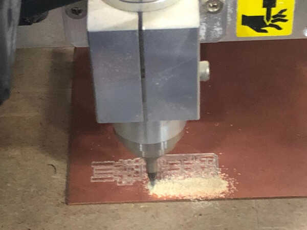
And here it is
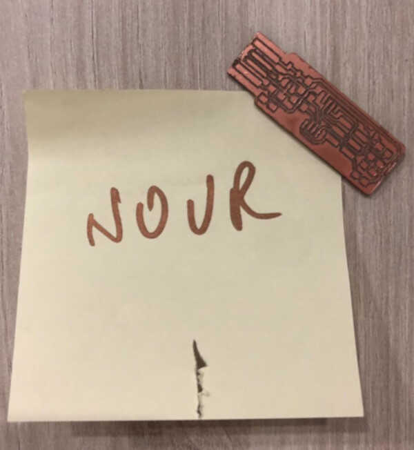
It took around 20 min all in all (internal and external path)
Now it is time to practice some soldering before doing it on the final ISP
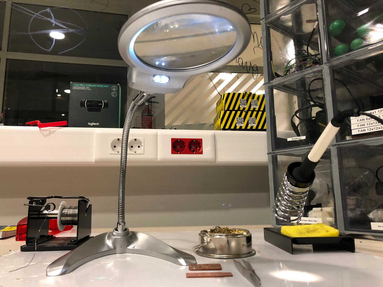
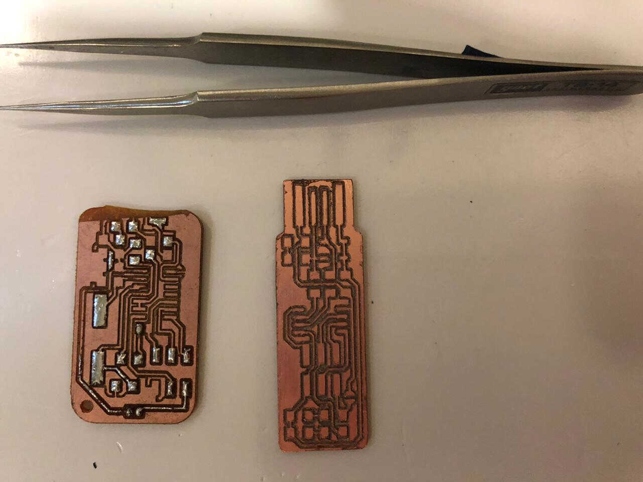
Prepare your workplace and your components and start welding, all while referring to Brian's page
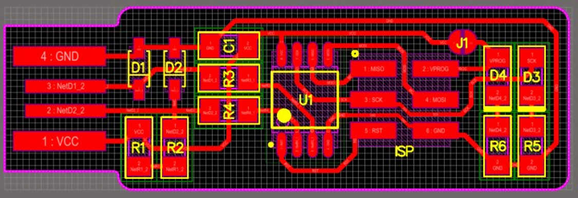
The components are the following in our case:
Keep referring to the below schemata while welding the components and pay attention to the orientation of each
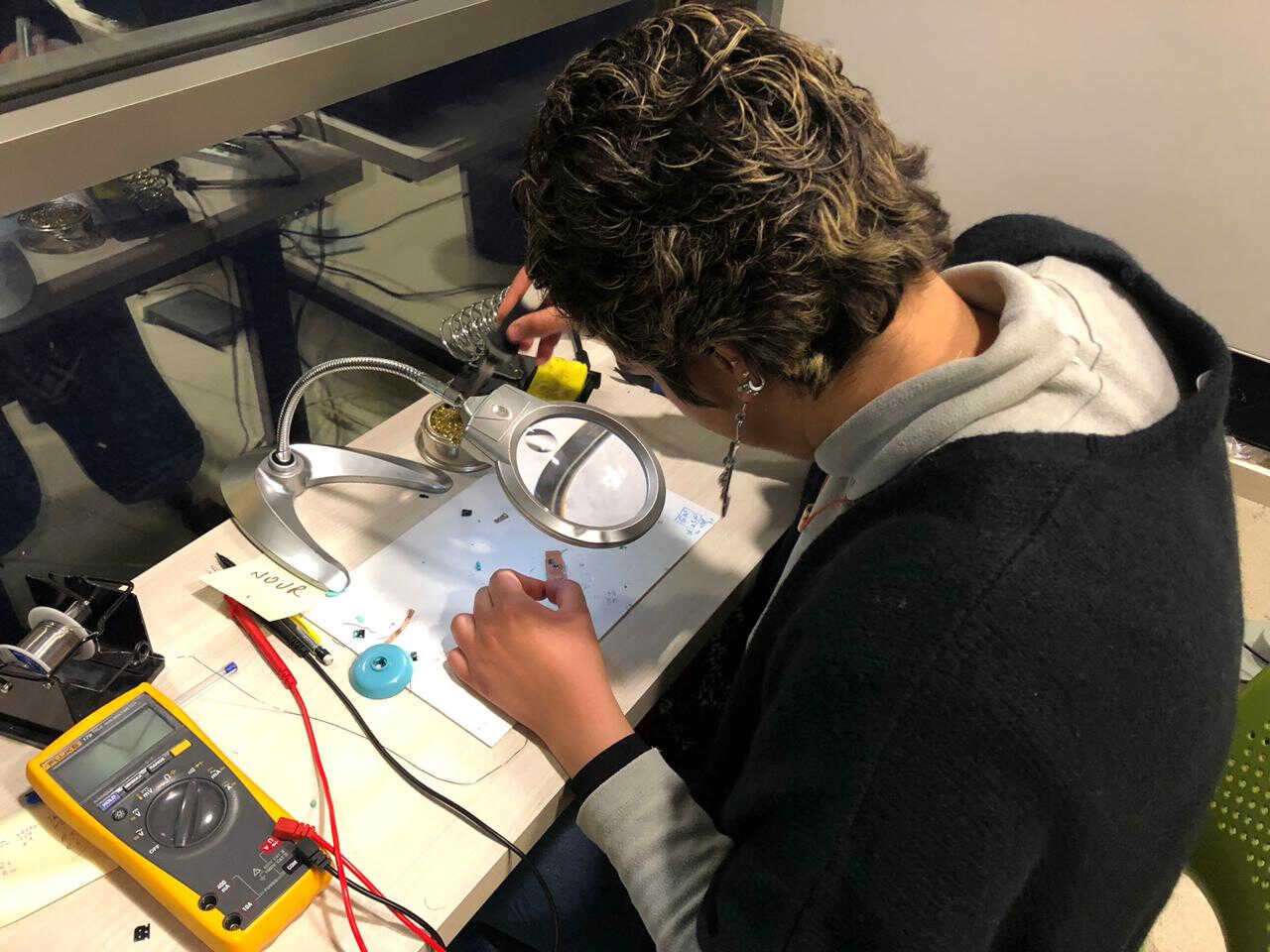
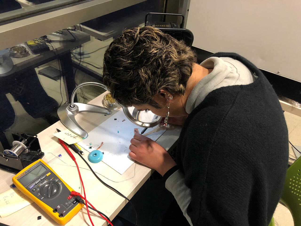


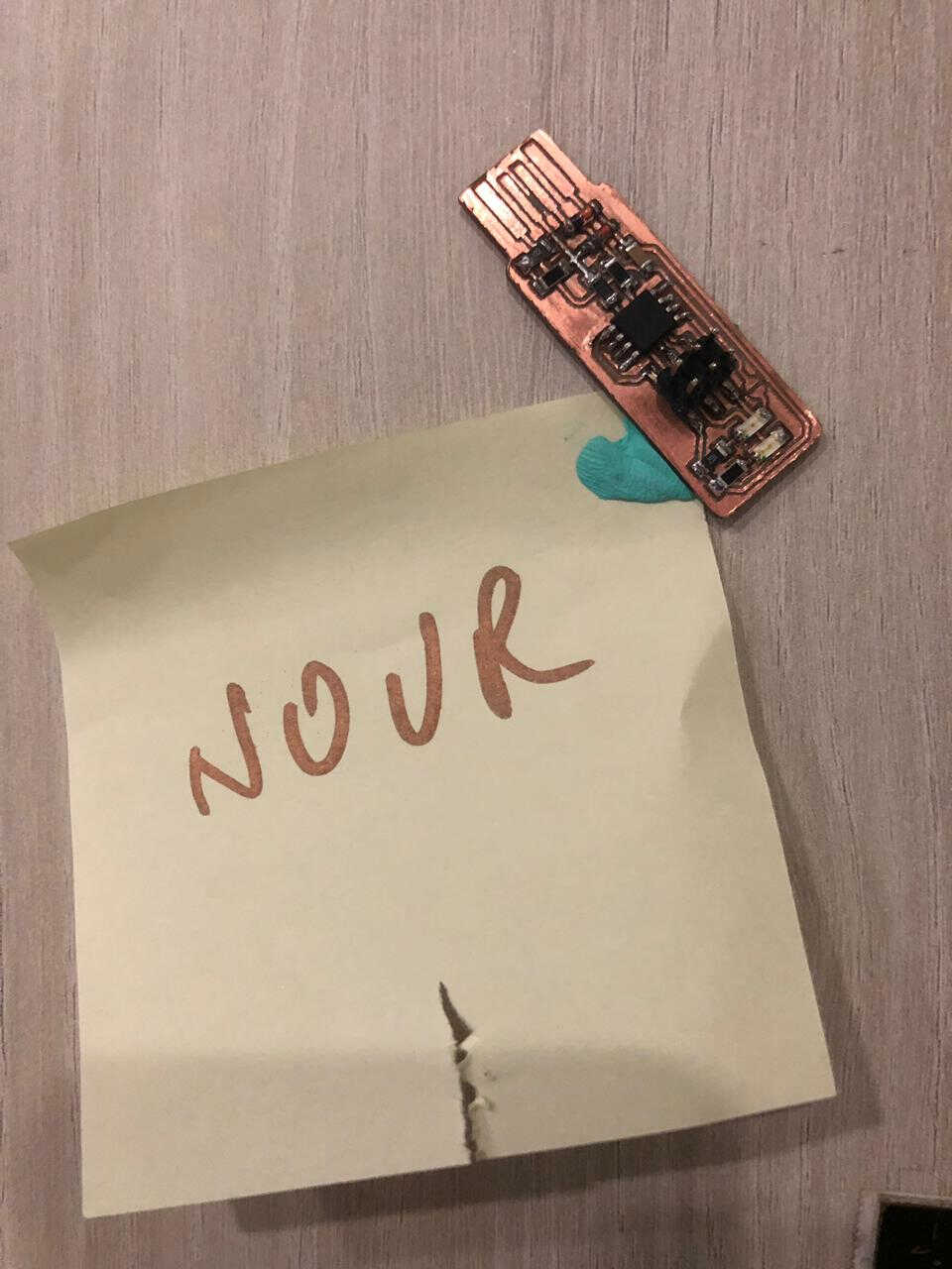
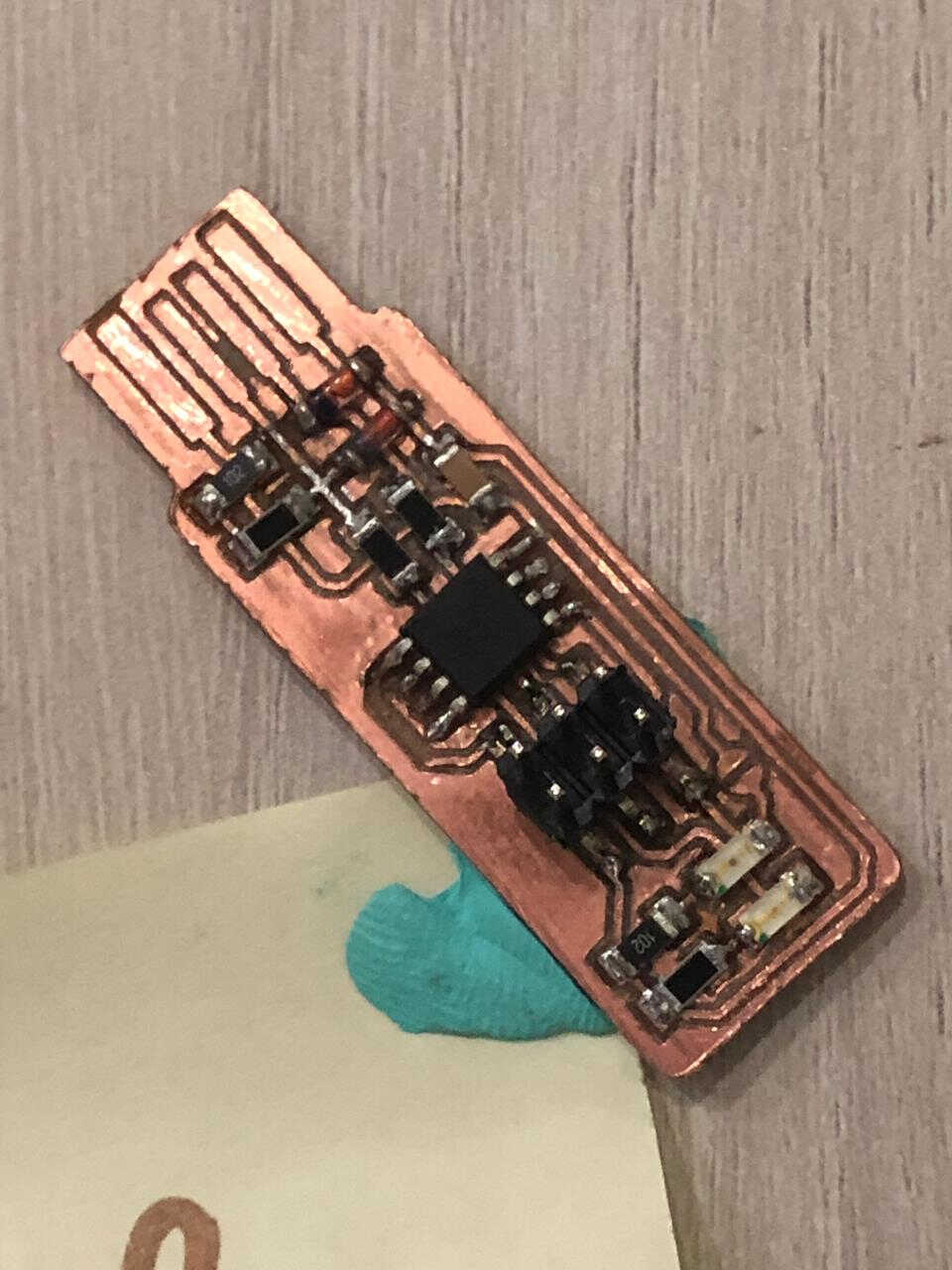
THE PROBLEM IS THAT THERE IS A PATH WHERE THE COPPER HAS BEEN REMOVED ACCIDENTALLY!

A very nice guy helped and sorted out the problem by adding a wire. It does not look very nice but it does the job -especially after checking every path with the multimeter
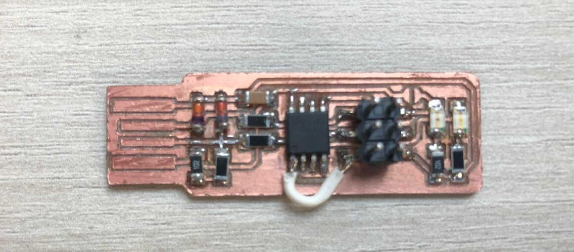
A very nice guy helped and sorted out the problem by adding a wire. It does not look very nice but it does the job -especially after checking every path with the multimeter and after the programming part
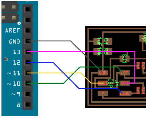
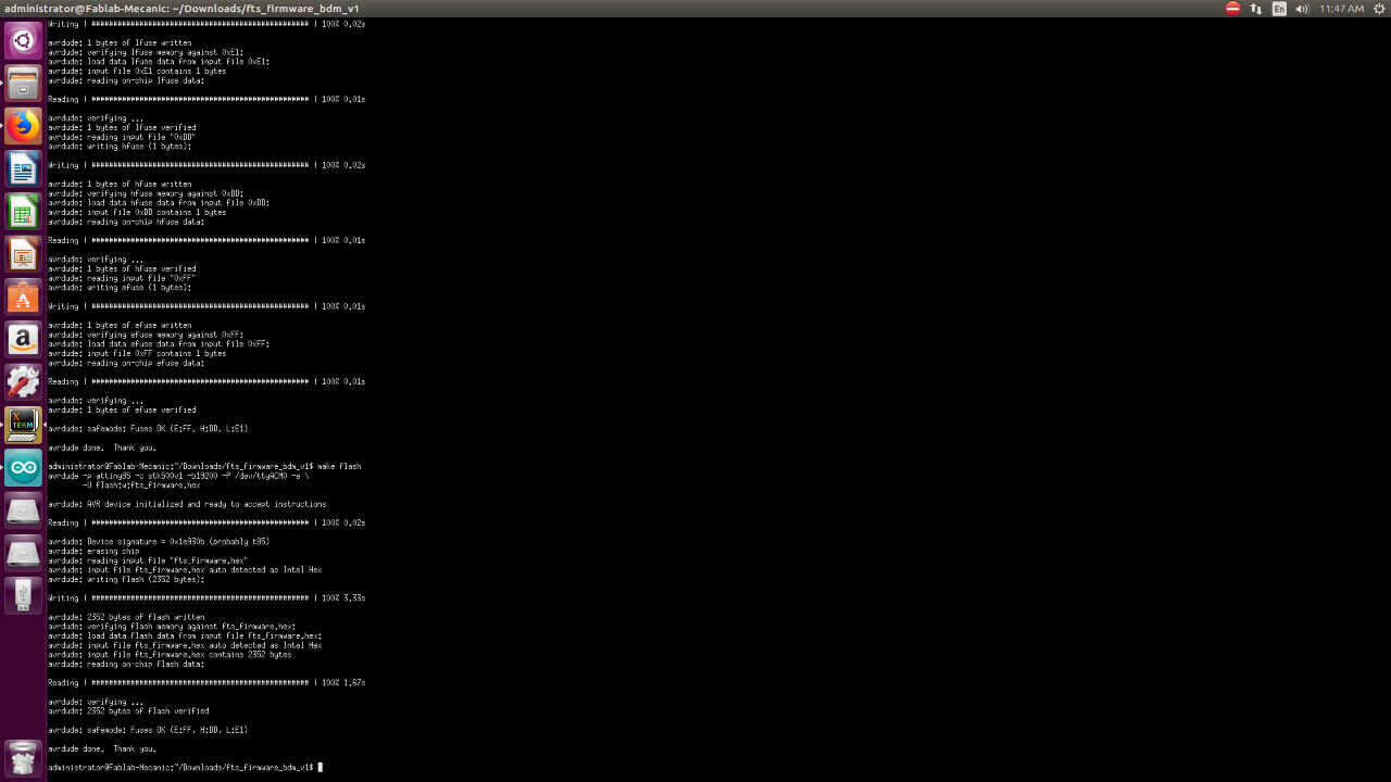
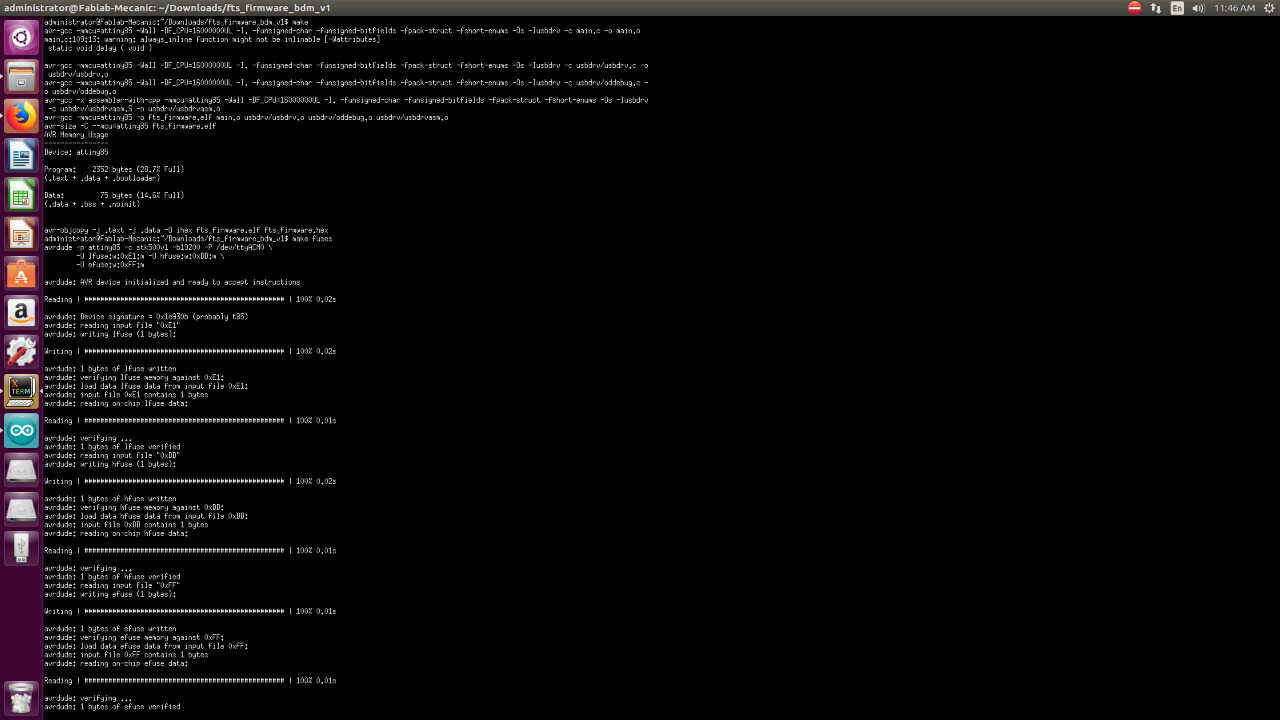
Now is the time for programming
G code of line test internal path
G code of line test external path
G code of Fab ISP internal path