experimentation
make it happen
Group Assignment - participants:Josep Marti, Felipe Santos, Alberto Lopez, Diar Amin, Gustavo Abreu
Fab Lab Barcelona have two different Roland milling machines
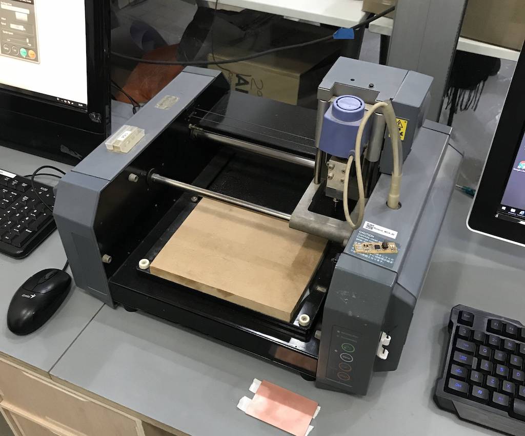
The Roland Modela MDX-20 is a small milling machine and a 2 1/2D precision scanner. This machine is mostly used for milling circuit boards, though it can also mill in other soft materials like machinable wax. For milling circuit boards you should export you design into a black&white monocroome png. For milling out 3 dimensional molds you should export your design as .stl The second use of this machine is scanning. It uses a thin needle to gently touch the object and calculates from this a 2 and a half dimensional model. Though slow at processing, it can create a high detailed model. Work area: 203 x 152 x 60 mm From wikipedia
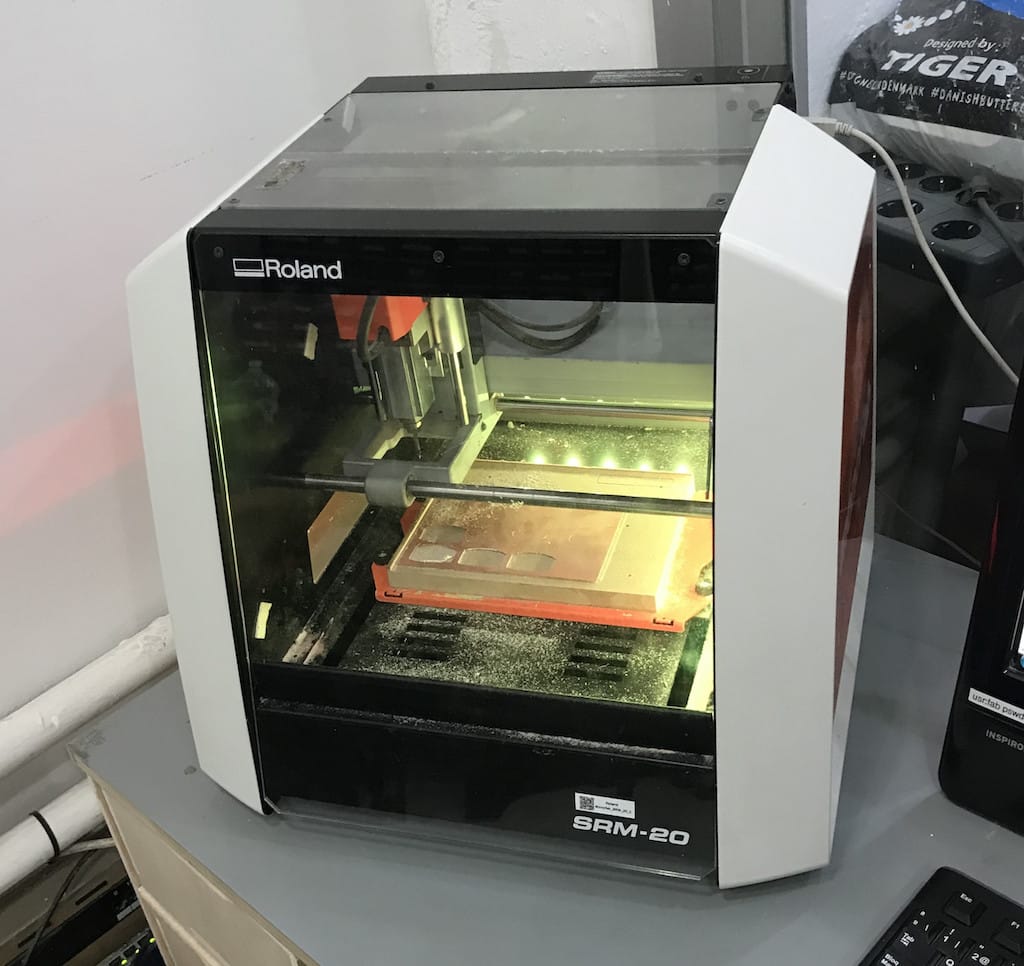
The Roland SRM-20 This machine is capable of cutting a wide variety of materials including chemical wood, acrylic, and ABS. It is also capable of a range of accuracy settings from prototype to product design. Plus its small size and fully covered design allows you to enjoy cutting more safely and with peace of mind. Work area: 203 x 152 x 71 mm from User Manual
Milling bits
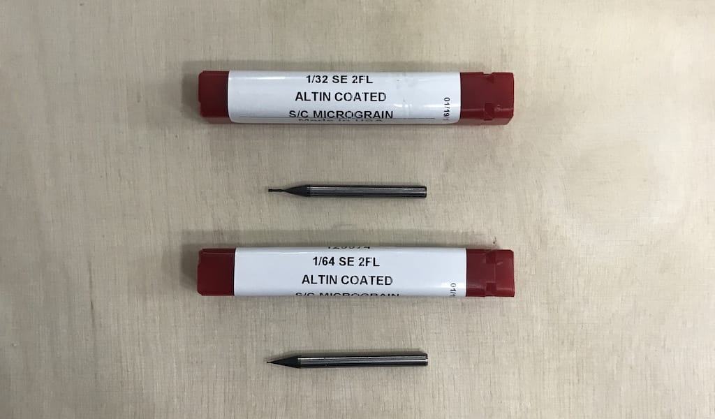
We have two different bits to work with our PCBs. 1/64” - Used for milling the trails on the board and 1/32” - Used for drilling holes and cutting the board
Softwares
Our instructors recommended us to test the machines generating files from two diferent softwares: MODS and Fab Modules.
MODS_link
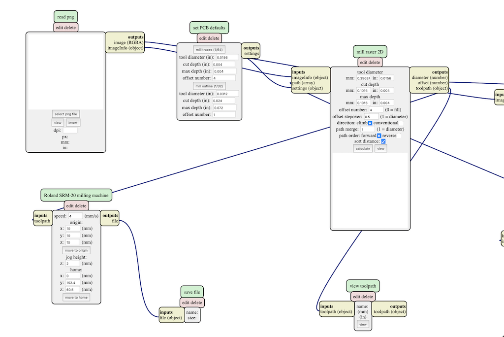
Right click program, open server program,machines, roland, mill, srm-20, PCB. Steps followed: 1. load png file 2. select trace or cut 3. change settings for the machine to origin 0,0,0 and home 0,0,5 (x,y,z) 4. delete the WebSocket module 5. add the save module instead 6. calculate path.
And then you’ll get the rlm file.
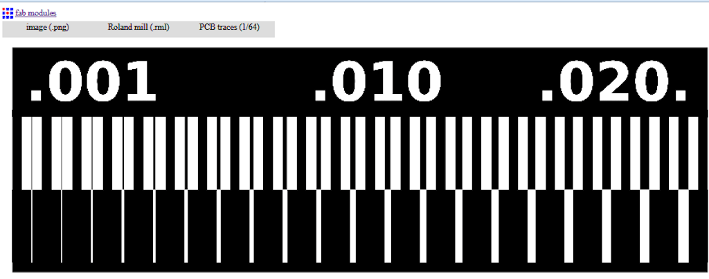
Fab Moduleslink
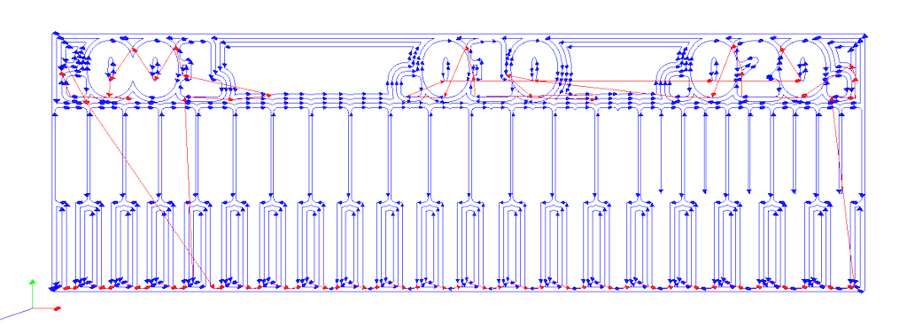
Download the line test documenthere
Click fab modules, than index.html and open the format png-document. Select Roland mill and PCB traces.
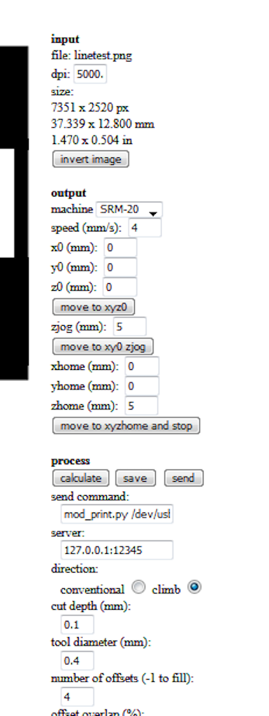
Insert settings:
Work file:
Now we do the same procedure with the outline cut. Dropping the “linetestinginterior.png” file into the Fab Modules. Same machine (Roland Mill) and different cutting (PCB Outline 1/32).
Process description
Choose the correct mill bit for the job and insert it into the machine. Than adust the z-axis “by hand”.
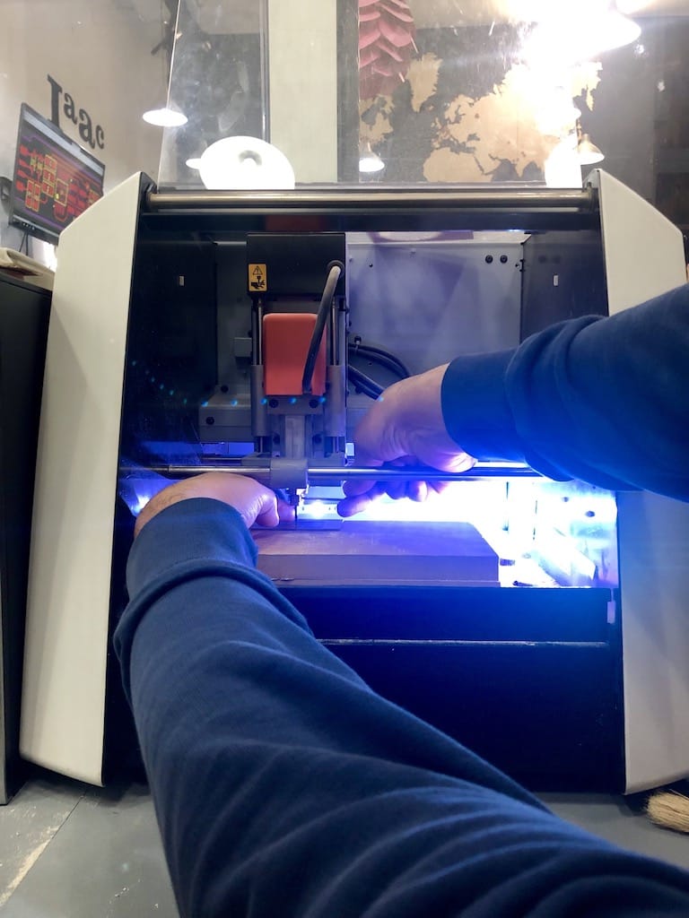
After that, set origin point for all axis
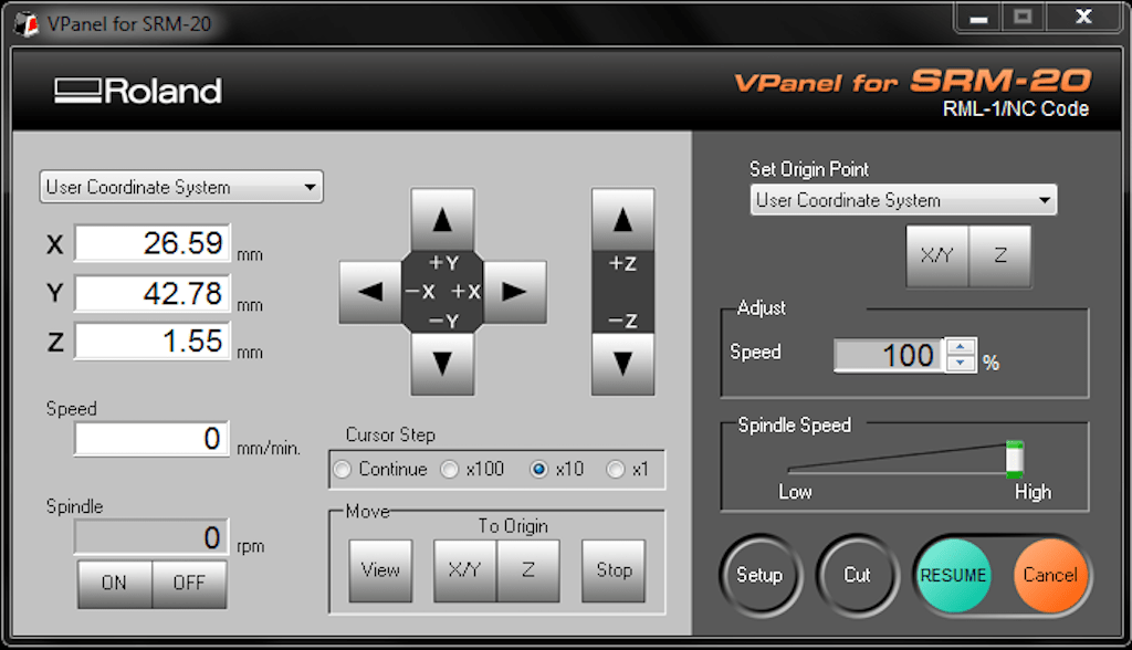
After that, set origin point for all axis
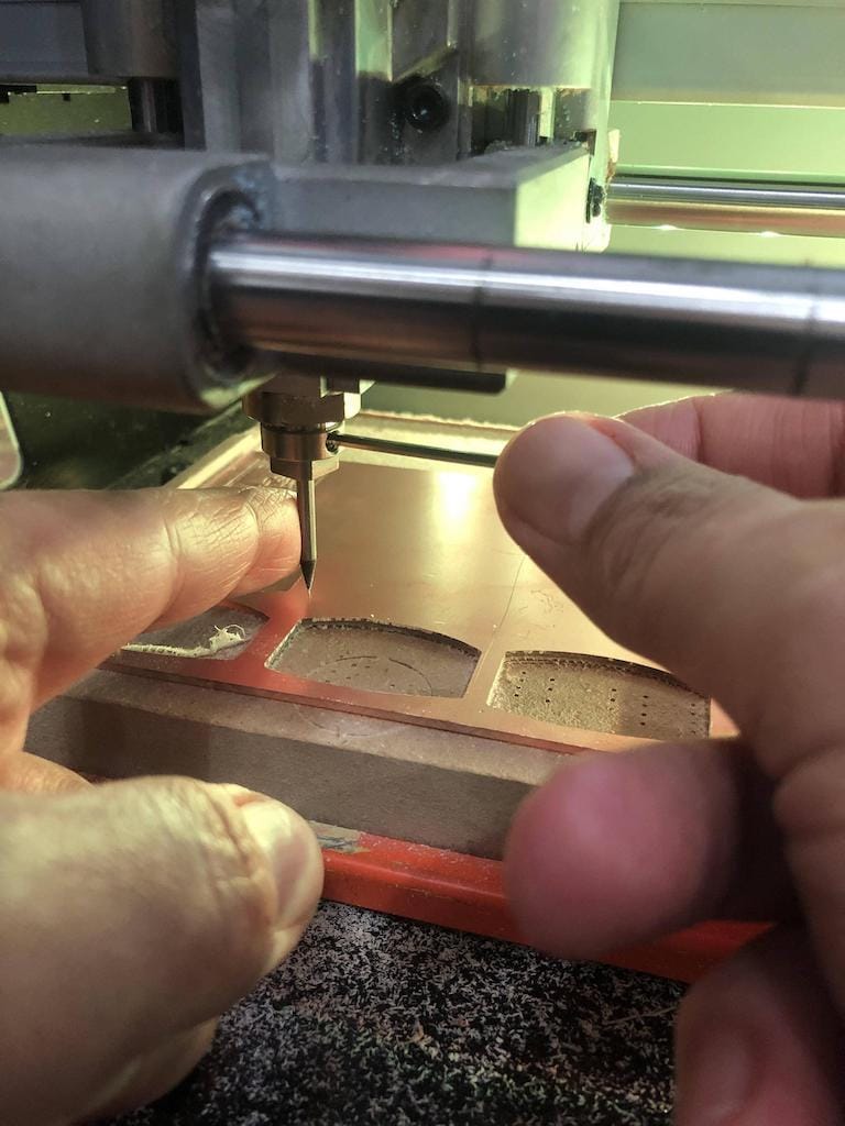
Then press “cut” to get to add the file “linetest.rml” and the job will start. Check if the milling goes well, not to deep, not cutting air. After finishing, just press view and it will bring the piece forward. Then we get the milled piece.
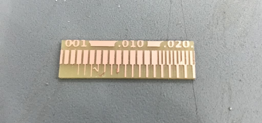
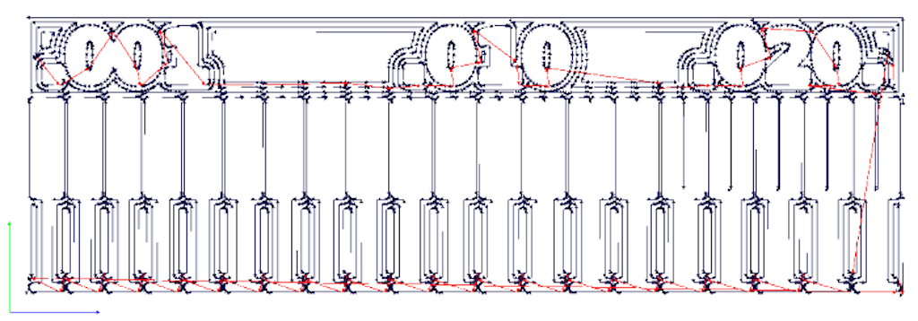
Compare results
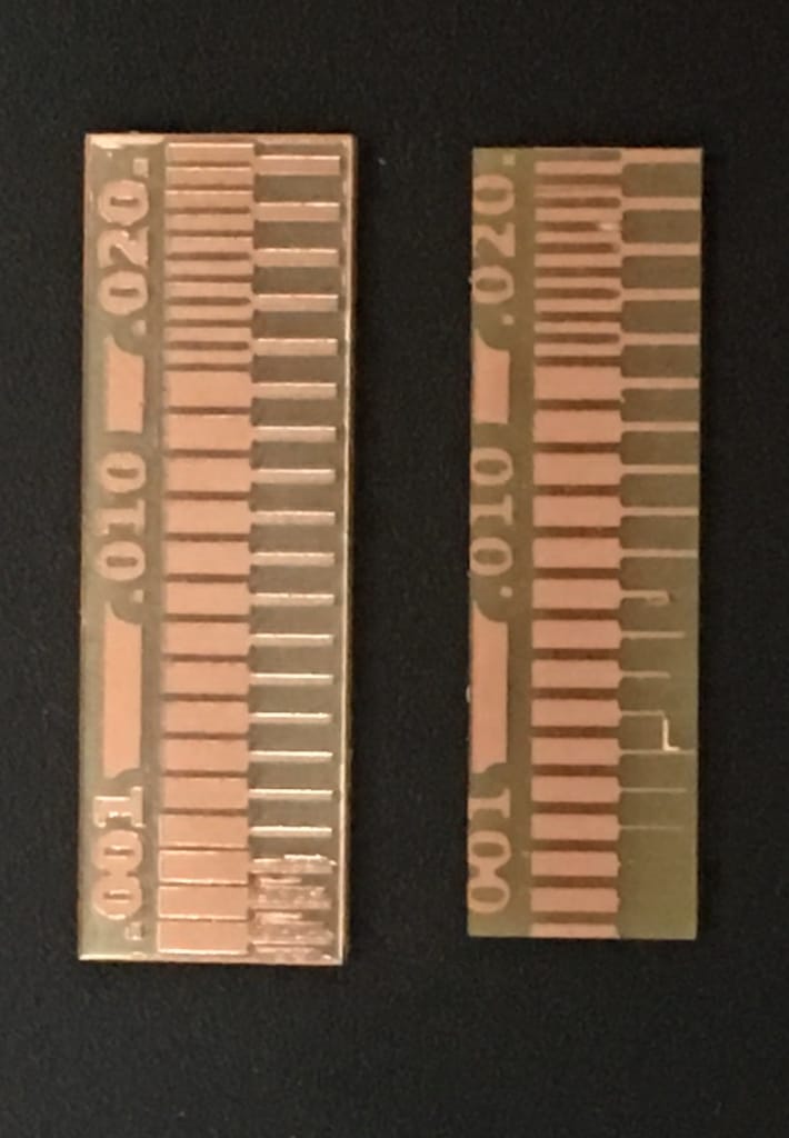
Conclusions
Using the same machine, bits and board; MODS presented better results. Begin able to mill up to .005 lines when fab modules only could do .011. So our software of choice for the rest of the process will be MODS.
Individual assignment
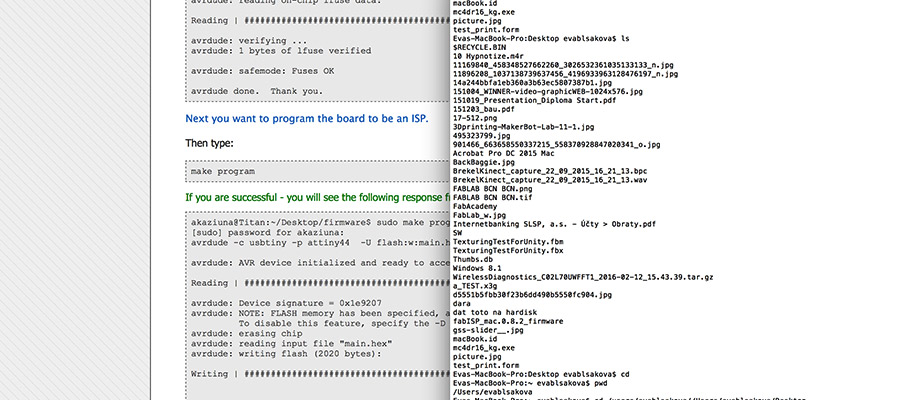
Here is a tutorial for creating PCB. FabAcademy Docs guiding step by step on how to build a FabISP.
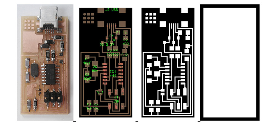
01_This is the goal - following Neils Example
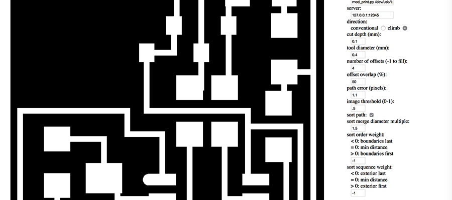
02_First upload the picture and re-check the size/resolution, than choose the machine in the output format. Make a decision which process is needed. See the options with the right drill besides. Change the tool for different process, of course, as we already did in the group assignment. Just follow the same pattern. Then we have to adjust the levels, ask for calculation, and save in order to put in in the IAAC Cloud.
03_Step back explanation - Before uploading my .png image we customized the board creating a personal label what we added in Photoshop (see the letter e). Settings in FabModules: we used x0,y0,z0 with a 0 value. xhome and yhome value 0 and zhome value 5. Cut depth 0.1 tool diameter 0.4 number of offsets 4 (you can fill the gaps using level -1), image threshold 0.5.
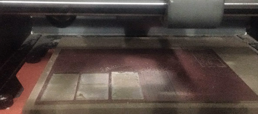
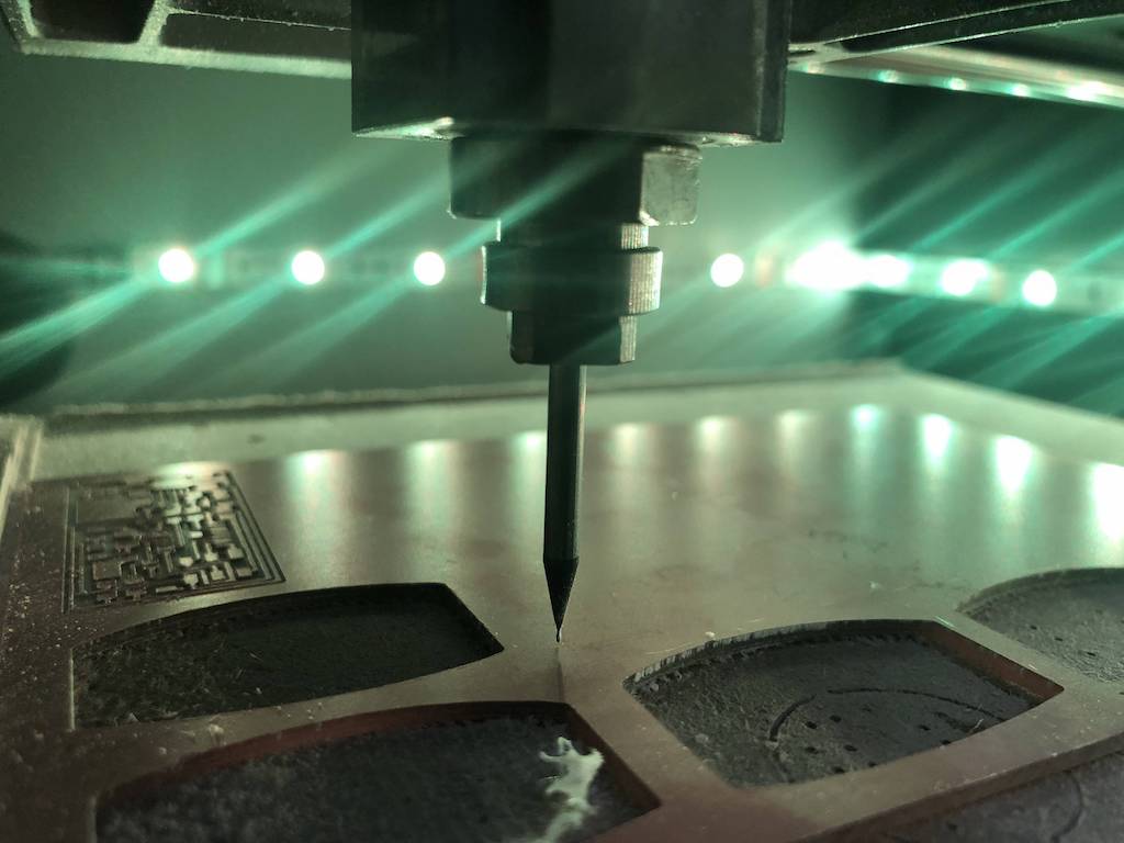
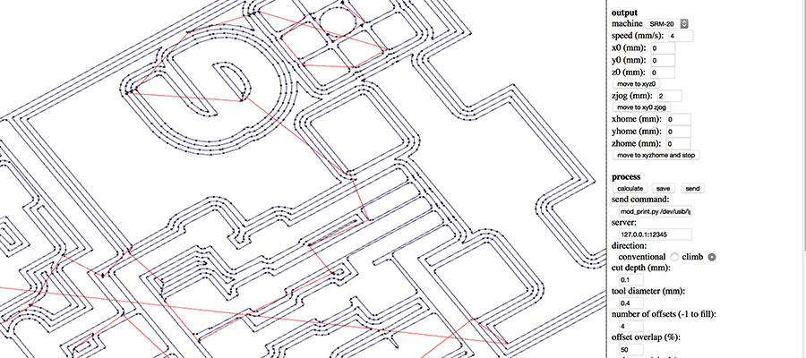
04_The procedure - the milling of the traces.
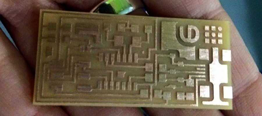
05_Finnished milled board, ready to adopt all components by soldering.
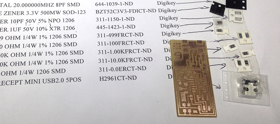
06_The information sheet specifies all components needed. Sticking them next to their description helps.
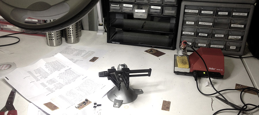
07_Assembling all components starting from the middle of the board, working towards the edges.
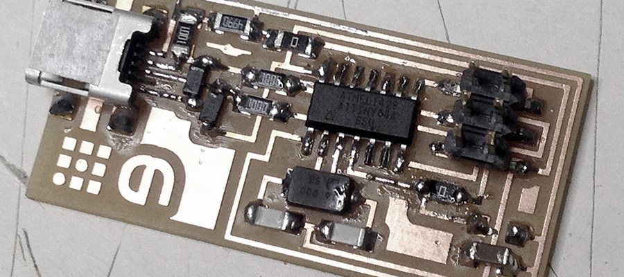
08_Final board with all components ready to be programmed.
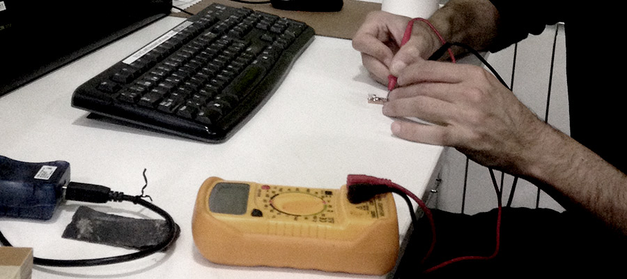
09_Next: Our Lab Instructor Ferdi helped me with debugging...with the multi-meter to check the connections between the components on the circuit board. - "beeping" through all connections to check if something is wrongly dis/connected.