
5.1. Introduction to electronic production
What is a PCB?
PCB is an acronym for Printed Circuit Board. It is a board that has lines and pads that connect various points together. Before the advent of the PCB circuits were constructed through a laborious process of point-to-point wiring. This led to frequent failures at wire junctions and short circuits when wire insulation began to age and crack.
Solder is the metal that makes the electrical connections between the surface of the PCB and the electronic components. Being metal, solder also serves as a strong mechanical adhesive. (Source: Sparkfun.com)
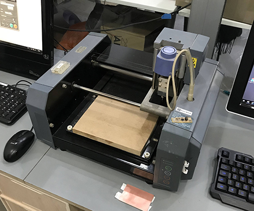
Milling machines
There are two different Roland milling machines in Fab Lab Barcelona:
The Roland Model MDX-20 is a small milling machine and a 2 1/2D precision scanner. This machine is mostly used for milling circuit boards, though it can also mill in other soft materials like machinable wax. For milling circuit boards you should export you design into a black&white monocroome png. For milling out 3 dimensional molds you should export your design as .stl The second use of this machine is scanning. It uses a thin needle to gently touch the object and calculates from this a 2 and a half dimensional model. Though slow at processing, it can create a high detailed model. Work area: 203 x 152 x 60 mm. (Source: wikipedia)
The Roland Model SRM-20 is capable of cutting a wide variety of materials including chemical wood, acrylic, and ABS. It is also capable of a range of accuracy settings from prototype to product design. Plus its small size and fully covered design allows you to enjoy cutting more safely and with peace of mind. Work area: 203 x 152 x 71 mm (from User Manual).
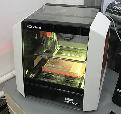
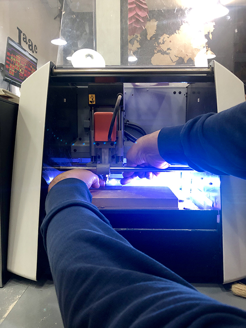
As the first one (Roland MDX-20) had some problems in terms of calibration, I chose the Roland SRM-20 milling machine.
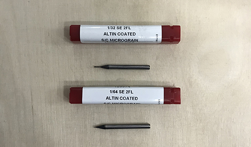
Milling bits
We are given two different milling bits to process the PCB. The 1/64" tip, to engrave the inner circuit, and the 1/32" tip, used for drilling holes and cutting the board's outline.
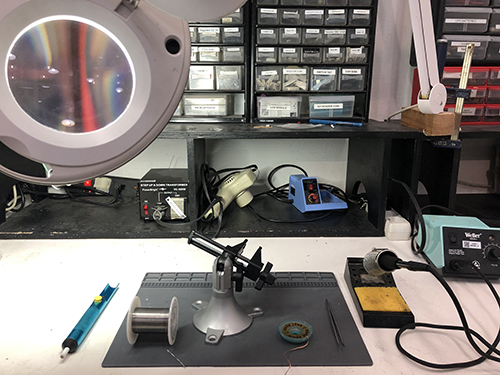
Electronic tools
These are some tools I used for the soldering process:
- A) Magnifier lamp
- B) Desoldering pump
- C) Tin soldering wire
- D) Soldering station
- E ) Desoldering copper wire
- F ) Tweezers
- G) Soldering stand base
- H ) Solder
- I ) Soldering sponge
- J ) Electronic components
Software
The software needed for the assignmet is the following:
- Illustrator: for editing or customizing the design of the board.
- FabModules or MODS: for creating the cutting files (.rml) attending to the necessary cut parameters.
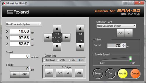
- VPanel for SRM-20 (Roland): for running the PCB cutting process.
5.2. Group Assignment
Autors: Josep Marti, Felipe Santos, Diar Amin, Gustavo Abreu and Alberto Martinez.
We first download the .png files from the documentation. Then work separately with both files to process the 2 works on the board.

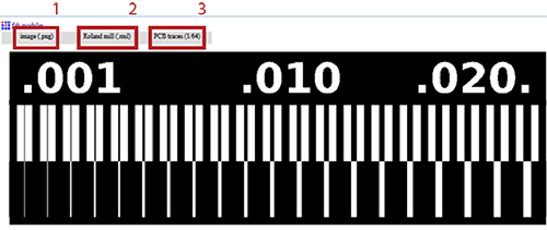
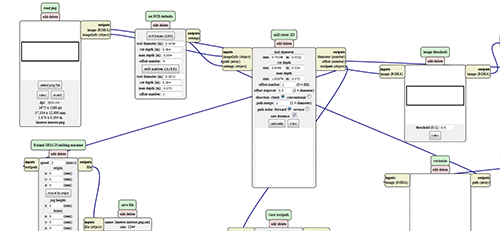
The first trial will be with FabModules. We need to load first the .png file on the program, and select the machine model and choose between traces and cuts.
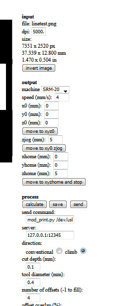
Then adjust the settings for the milling axis, setting the speed (we may need to change from 4 to 3mm/s), zjog (height of the mill to change from path to path), home location and the calculate the path.
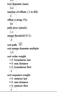
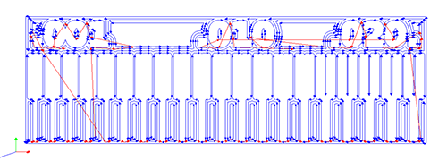
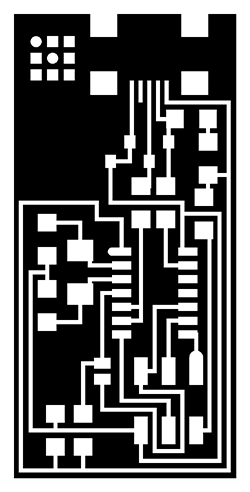
This is the .rml file calculated by the program:
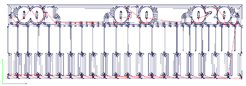
On the 3D view, we can see how probably the lower part of the outline may fail on cutting due to the path calculation.
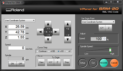
After setting the origin point for all axis, we drag the .rml file into the milling machine's software (Cut > delete all old files > Add new .rml file), and adjust the machine's parameters.
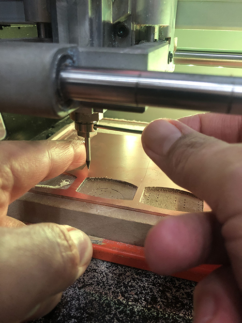
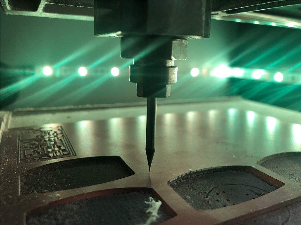
First we set the copper board on the working area of the milling machine.
XY and Z (this last one must be adjusted manually)
We can appreciate, how the outline wasn't cut propperly due the cutting path set on the .rml file created with FabModules.
Then we change to Mods. While opening the website, right-click on the site to start a new program, open the server program and select the machine model and the milling bit.
The steps to follow are:
- Load first the .png file- Select to trace or cut.
- Change the settings for the machine to origin (0,0,0) and home (0,0,5), to prevent from dragging the mill over the PCB.
- Delete the WebSocket module.
- Add a save module instead.
- Calculate the path.
- Then we get the .rml file:
Check if the milling goes well, not to deep, not cutting air. After finishing, just press view and it will bring the piece forward.
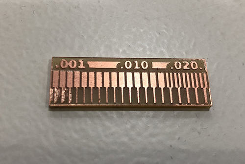
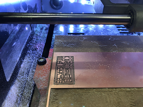
Then we get the milled piece:
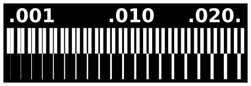
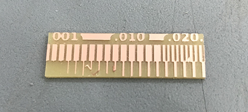
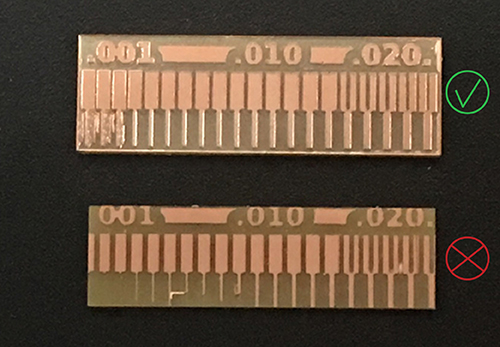
After comparing the results, we can see that using the same machine, bits and board; MODS presented much better results. Begin able to mill up to 0.005 lines when fab modules only could do 0.011.
Actually to solve the problem on the FabModules, we had to invert the outline .png file so that the path could be joint correctly. Anyway, the quality of cutting would be finest with the MODS path calculation.
5.3. Individual Assignment
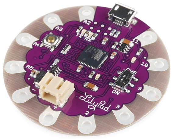
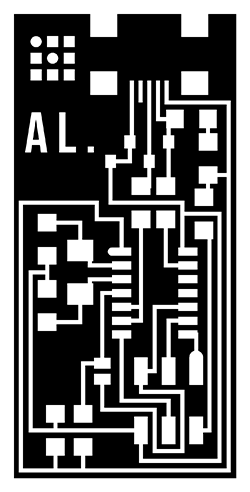
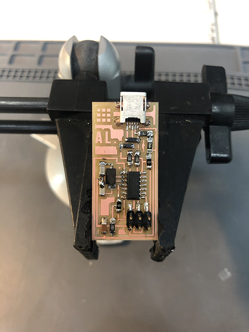
For the individual assignment, I chose to modify and program the Hello.ISP.44 PCB.
Grab .png file from the documentation.

I added a my initials to persolanize the design of my PCB using Illustrator:
I opened the file with mods, and followed the same steps as in the group assignment with both, interior and exterior parts. Then, the .rml file was generated with the software. And finally, opened Roland software and added the new file.
Cutting process
For the cutting process, after setting the position for the 3 axis, I set the order "Cut" on the Roland VPanel Software, and the milling machine starts cutting the inner part with the 1/64" milling bit. Then repeat the same proces for the outline .rml file, changing to the 1/32" milling bit in the machine.
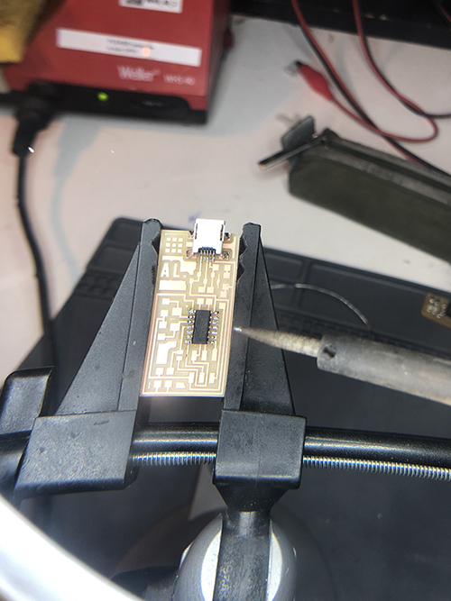
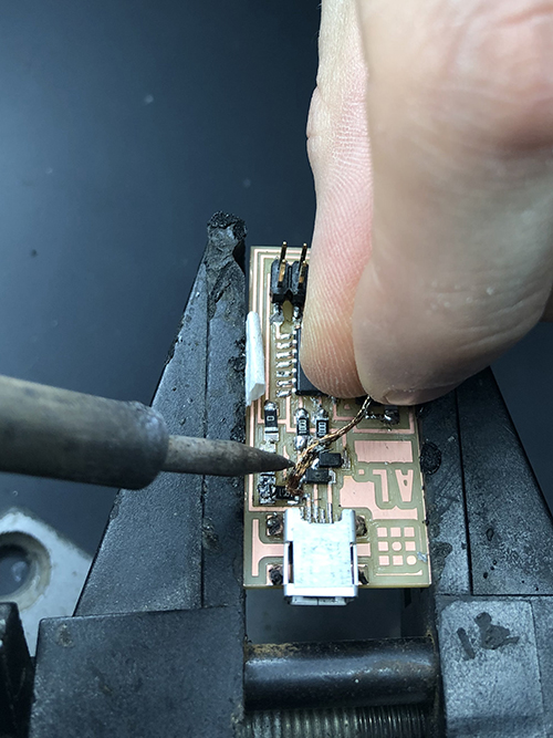
Soldering process
First I take into consideration the scheme of components and connections of my Hello.ISP.44 board:
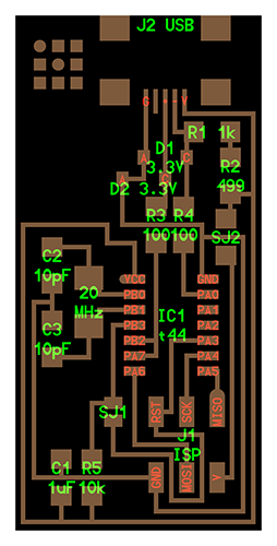
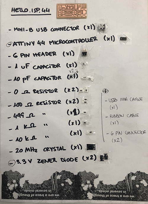
List of materials:
- Hello.ISP.44 board (x1)
- Mini-B USB connector (x1)
- ATTiny 44 Microcontroller (x1)
- 6 pin header (x1)
- 1 uF capacitor (x1)
- 10 uF capacitor (x2)
- 0 ohm resistor (x2)
- 100 ohm resistor (x2)
- 499 ohm resistor (x1)
- 1 kohm resistor (x1)
- 10 kohm resistor (x1)
- 20 MHz crystal (x1)
- 3.3V zener diode (x2)
And placed all the elements onto a paper:
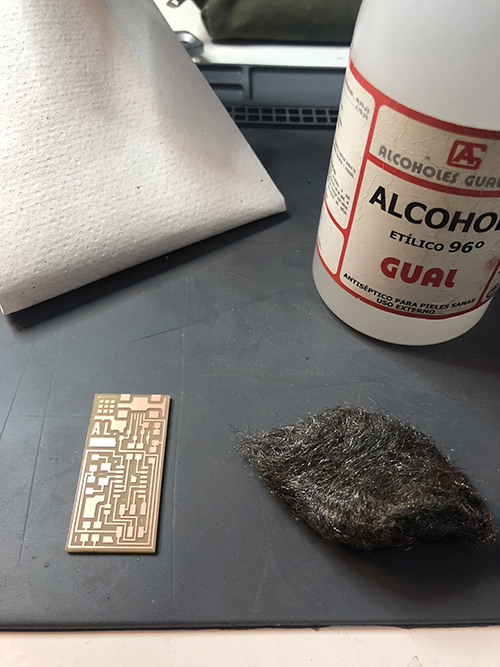
Clean the surface softly with alcohol and steel wool to avoid dust or any material left from the cutting process. Then start soldering the different components onto the PCB.

A soldering station and a magnifier lamp may help to work more comfortable with the rest of the tools.
How to program it?
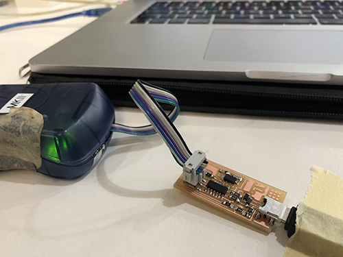
First I need to check conductivity, to confirm that all connections are fine, and there won't be any problem with shortcuts that may injure any component.
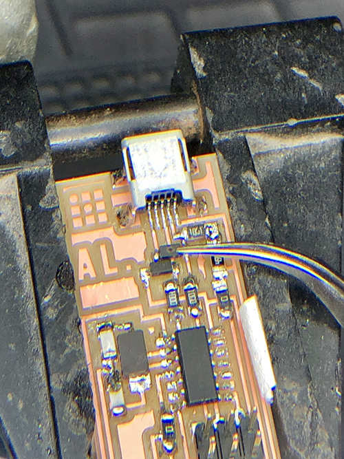
I burned one zener diode so I had to replace it with a new one.
Finally, after testing all connections are OK, I followed the steps to program my PCB shown here.
This means, first, installing the necessary software for my OS (as I already have my XCode installed, I just need to download the Crosspack AVR) and download the firmware.
Then, open the terminal and unzip the firmware.zip directory (cd ~/Desktop > unzip fabISP_mac.0.8.2_firmware.zip), and enter into the new directory created on my desktop.
To power the board, I need to plug the mini USB connector for the FABISP into my computer. Parallely, plug in my ATAVRISP2 prgrammer into the 6-pin programming header. As I'm using this programmer, I don't need to edit the Makefile with TextEdit.
And at last, to compile the firmware, I typed on the Terminal "make clean", with succesful response, then "make hex"; to set the fuses so my PCB will use the external clock (crystal), I typed "make fuse"; and to program the board as an ISP, "make program".
Then check on the "About this Mac" Menu, if the FabISP USB appears correctly on the USB-tree hub.
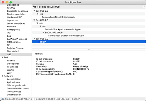
The PCB is successfuly programmed!
After programming the board, 0 ohm resistor and solder bridge must be removed. With the help of the desolding copper wire and the pump, once heating up first the tin, I take out both components from my PCB.
Now my PCB is prgrammed and ready to use!!