This assignment gives the student experience on connecting devices such as a switch and a LED to a Micro-Controller Unit (MCU). It also goes through PCB fabrication by milling with a CNC mill. This is an important experience as an introduction to automating machines by creating a circuit which receives programming instructions in order to control output to and receive input from external devices.
I could find freedom-enabling software to design electronic circuits: KiCAD and Fritzing. I have tested the former. But the later looks very easy to use and could be a better introduction for newbies.
KiCAD is libre software suite of programs for automation of electronic design. Each program of the suite is independent. But it works with the workflow of the others. It is an advantage for its modularity. Nevertheless, it is a problem for learning because the workflow from one program to the other is not as intuitive as I would like. But the most important for me is that it is libre software. So, it is under my control to learn and contribute the functionality I need or the funds for developing them. KiCAD also has the advantage of being able to use group edited libraries.
Install KiCAD
guix package -i kicad
Then I installed a dependency for KiCAD to function properly (Guix is beta software).
guix package -i libxslt
I also installed other PCB manufacturing softwares for testing purposes.
guix package -s pcbguix package -s qucs-sguix package -s fritzingLibraries of the components in the FabAcademy inventory are available. They contain the files needed for the placement of the electronic connection pads, the type of component they are and the way they look along with labels to their function and their connection pads.
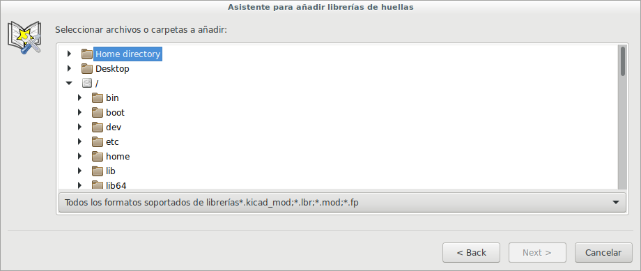
Download the libraries for KiCAD. You can also clone the git repository with:
git clone https://gitlab.cba.mit.edu/pub/libraries.git
. If you clone you can collaborate and get the latest versions easily. But I only downloaded the libraries.
Then I decompressed the libraries with
tar xvf libraries-master.tar
Entered the decompressed directory
cd libraries-master/
And moved only the KiCAD libraries to my website repo:
mv kicad ../../ramiro-ordonez/skizoj/kicad_libraries
Then I changed to the upper directory and deleted all the other libraries.
cd ..rm -fr libraries-master
I later found out there was an update to the FabAcademy libraries for KiCAD on Emanuele Goldoni's FabAcademy 2017 website. I have described how to intall it on my Input Devices page.
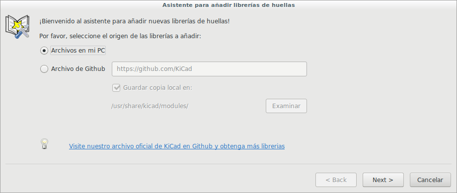
You can either add a local file or a web file. The latter allows automatic update of parts' libraries. It is a handy resource.
In order to use a component, we must be sure to feed it the right voltage and that the current that goes through it does not exceed its capacity.
The MCU datasheet specifies the Micro-Controller Unit operation voltage. We can use it for calculating the value of the resistor that is connected in series with a LED we want to use.
VR = V MCU - VLED
R = VR / iLED
If you want the LED to glow dimmer, you can add a higher value resistor. Just multiply the calculated value by the factor of brightness you want ( 0.1 ~ 1.0 ).
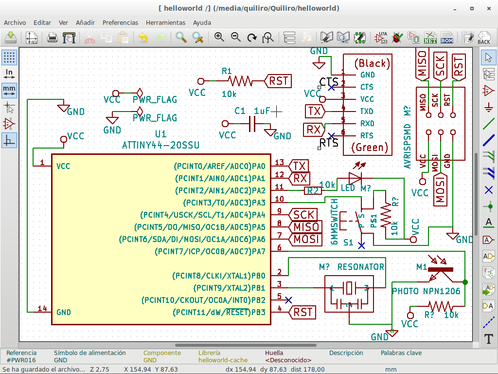
Then you can draw the schematic with KiCAD's Eschema. You can open it from the project window.
Once there, add each component by pressing the Add symbol icon on the left of Eeschema window.
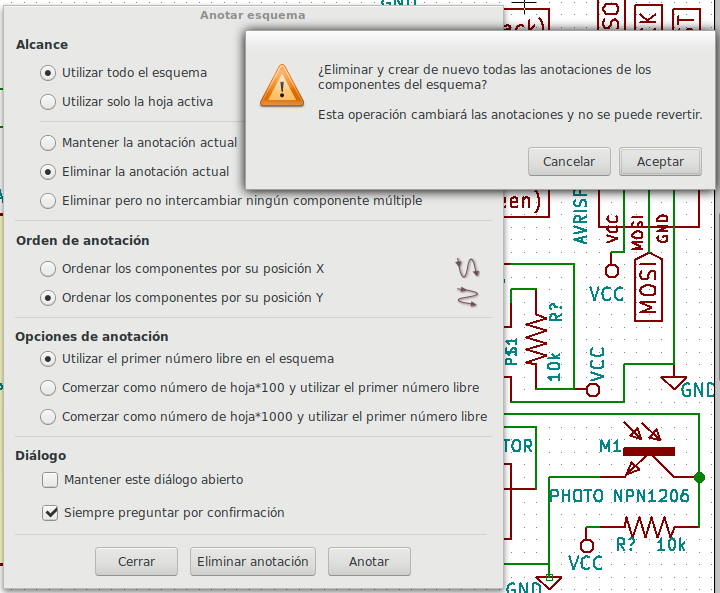
In order to have the software relate the component footprint to their names and values, we must anotate the components by clicking the following icon.

So it asks the way and order to label the components.
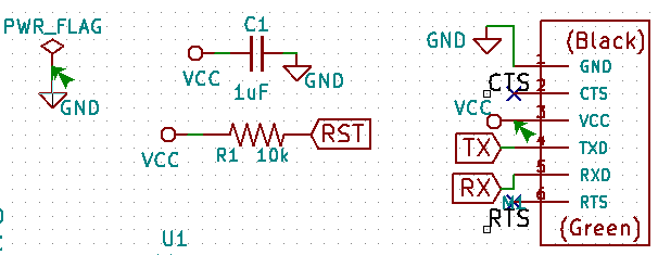
It is easy to connect one component with one or more other components by placing the same label on them. Then you do not have to bloat the schematic diagram with spagetti connection traces.
With the threads and the labels we connect all components.
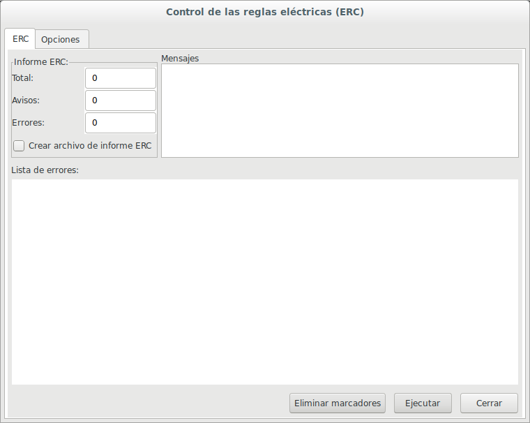
ERC (Electrical Rules Control) icon allows the software to check that all components are connected.

It opens a window which reports the errors encountered.
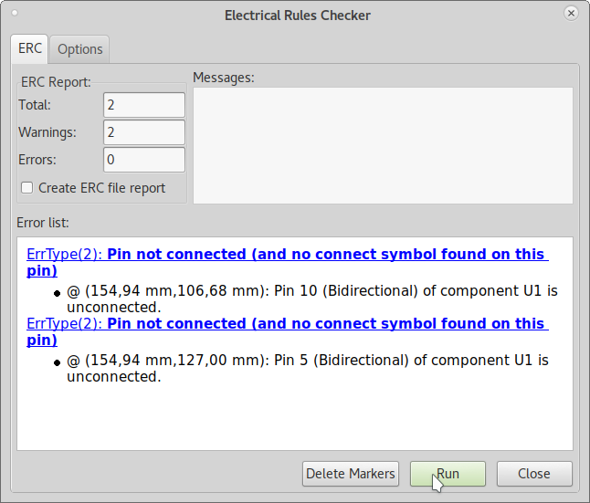
And signals the places in the schematic diagram.
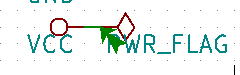
This power flag had no component to power.
This switch had one of its connectors disconnected.
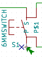
I proceeded to connect the power flag to a component and to mark the switch connector as unconnected. So the software gave no more errors after these 2 corrections.
In order for the software to create a view of the real PCB, we must asociate the components in the schematic with the footprints showing their shapes and their connectors. Each component has a specific drawing that must be related to it.
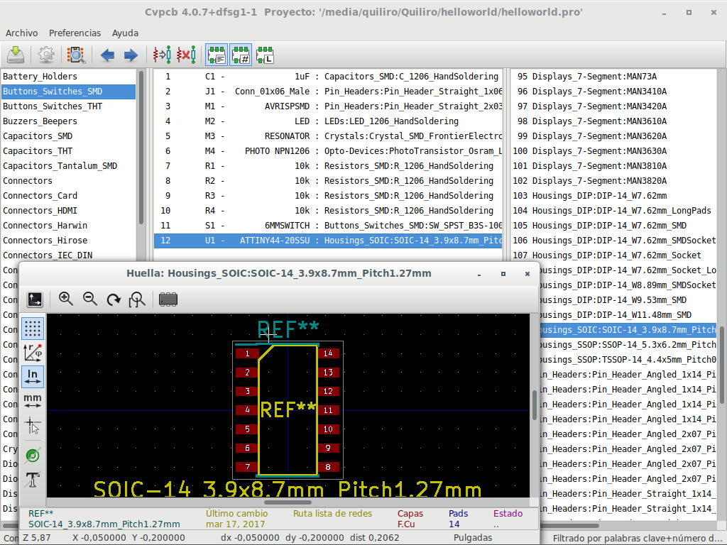
So the anotations can place the components on the drawing for connecting the components. We press the netlist icon.

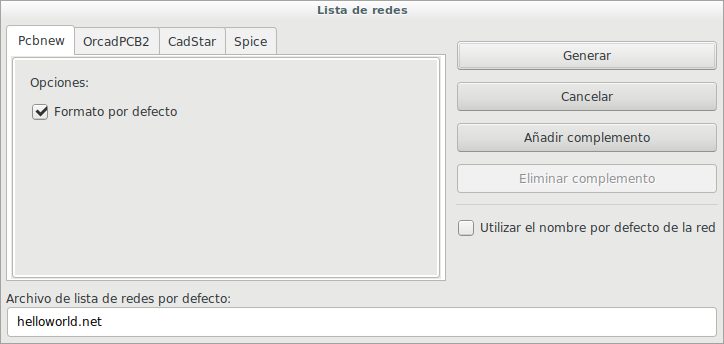
The netlist is the list of the components, their footprints and their connections. We press the Generate button in order to produce the netlist.
We can now trace the tracks. This is done by opening the PCBnew program. The icon is one of the last on the icon bar. So it opens a window with a lot of layers. We will focus on the cut layer (B.Cu) and the copper layer (F.Cu).
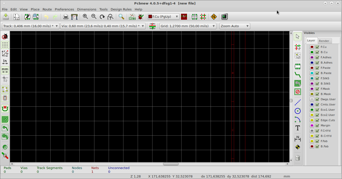
We choose the Netlist icon in order to import the netlist. And specify the path where the netlist was saved.
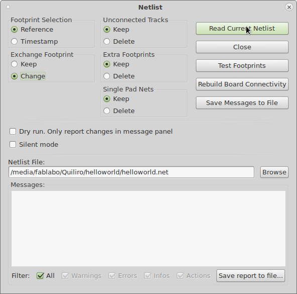
Then we press the Read Current Netlist button. (I had errors because I did not load the footprint library. What I loaded before was the component library in order to anotate the components.)
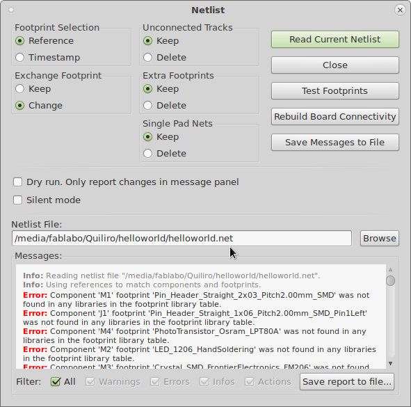
So I download the component footprints from Emmanuelle Goldoni's Fabacademy website as I mentioned above.
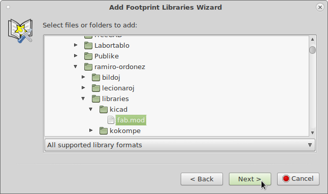
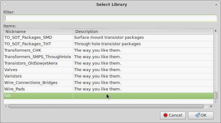
I confirm the changes to the library.
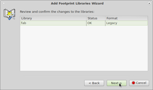
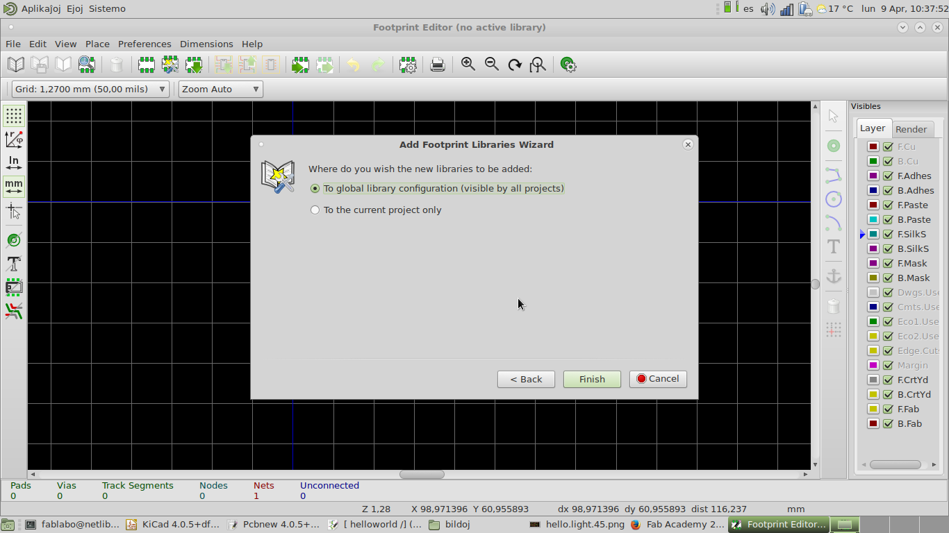
And add the library to the global configuration.
I have this library visible now. It is best to remove the other libraries to avoid confusion.
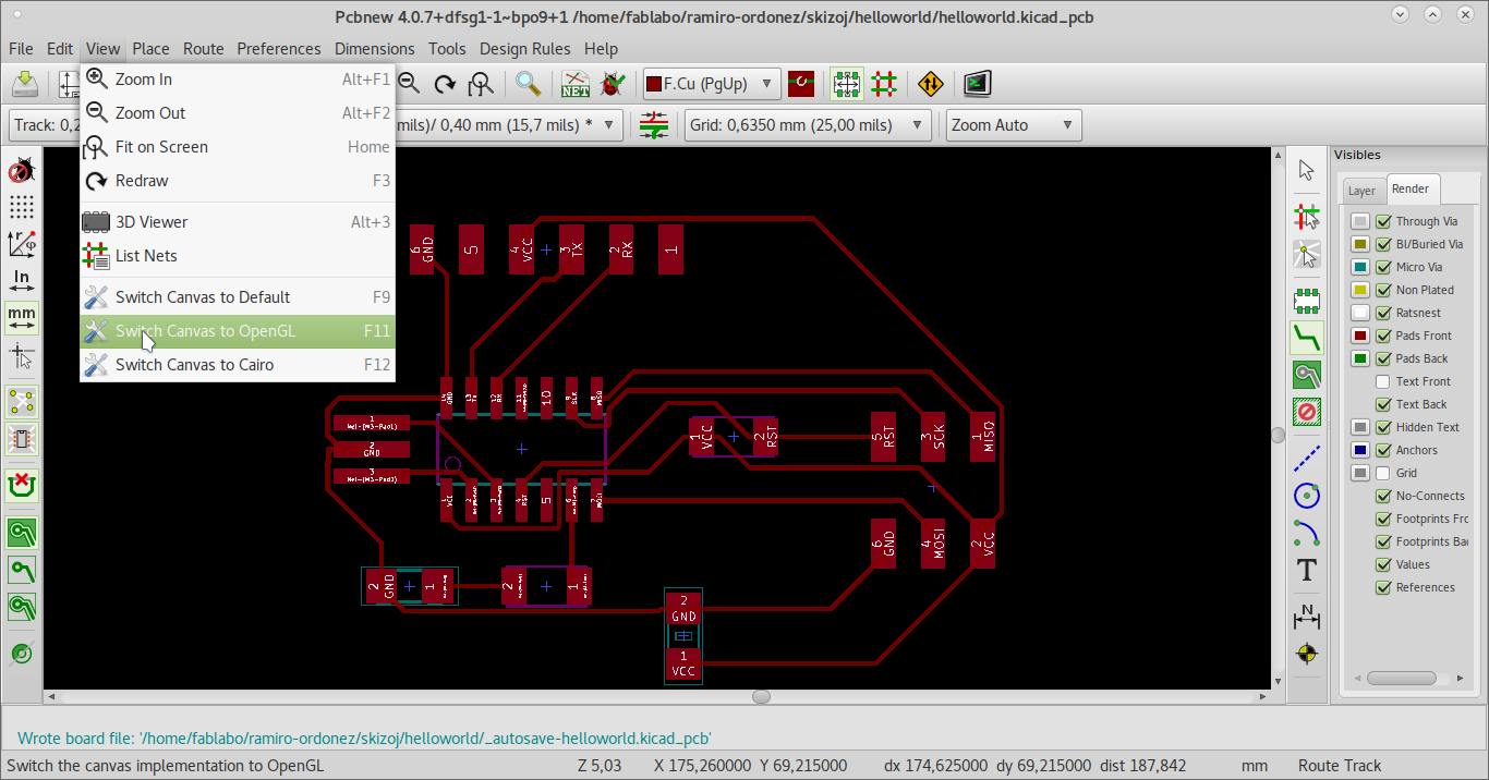
Switch canvas to OpenGL in order for the traces to automatically flow around and into the other connections.
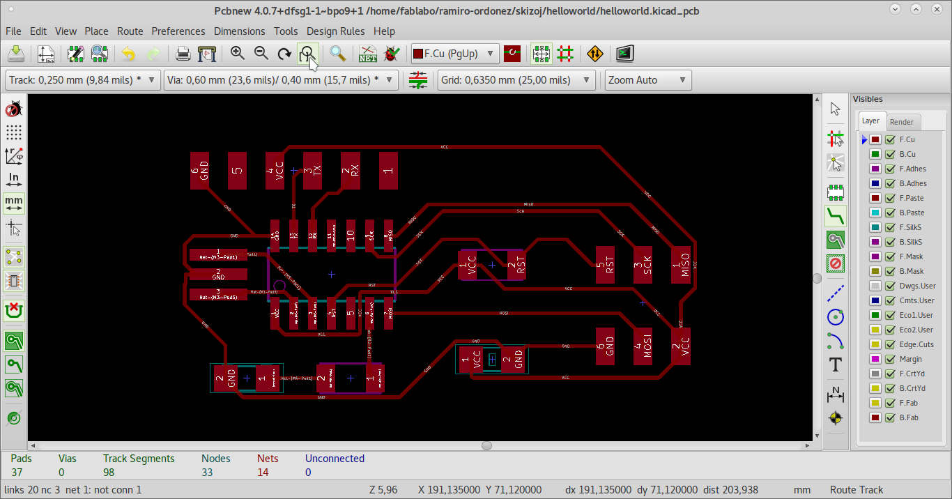
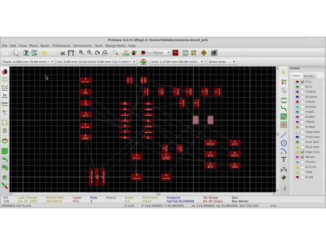
The connections were traced.
The final traces and the edge cut were drawn. Also the identification marks are visible in this picture.
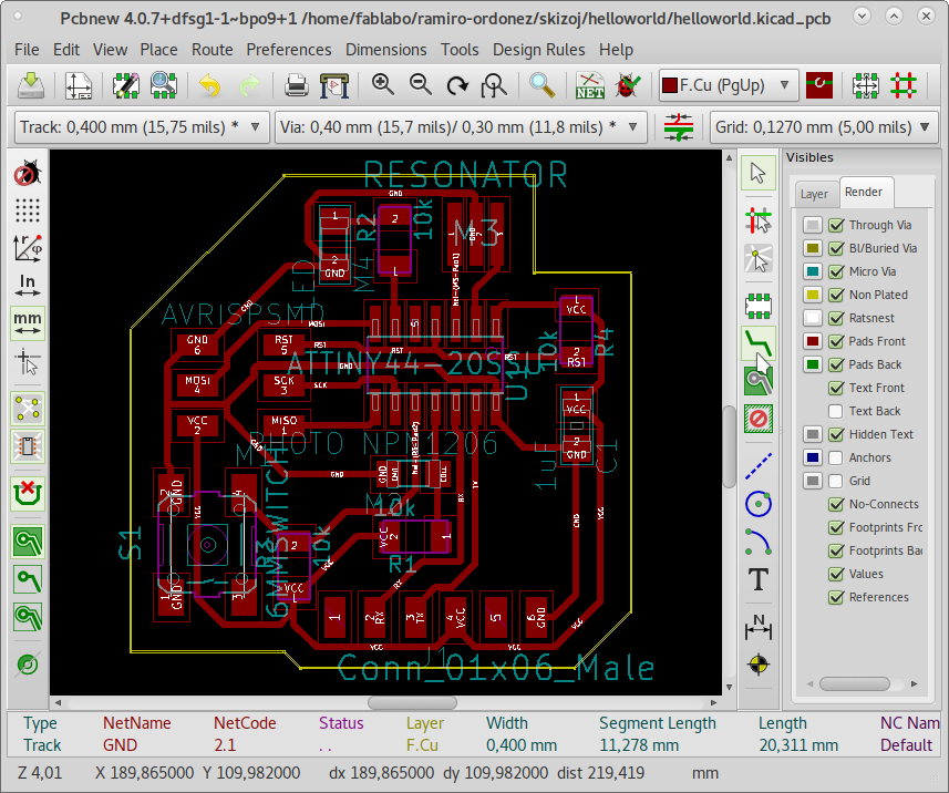
These are the many steps taken to accomodate components and traces in order to connect them all.
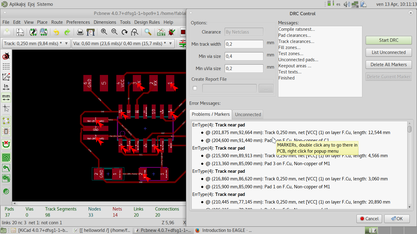
The design rules are checked in order to verify that all connections are made. Design Rules Checker (DRC) reports the unconnected components until these problems are solved.
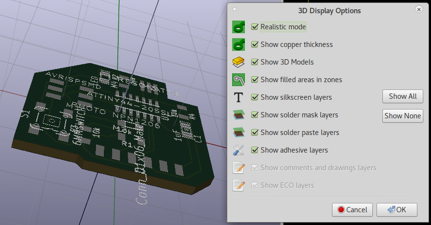
A render is shown.
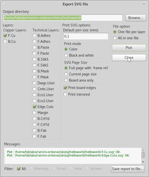
The edge cut layer and the copper layer are exported to SVG.
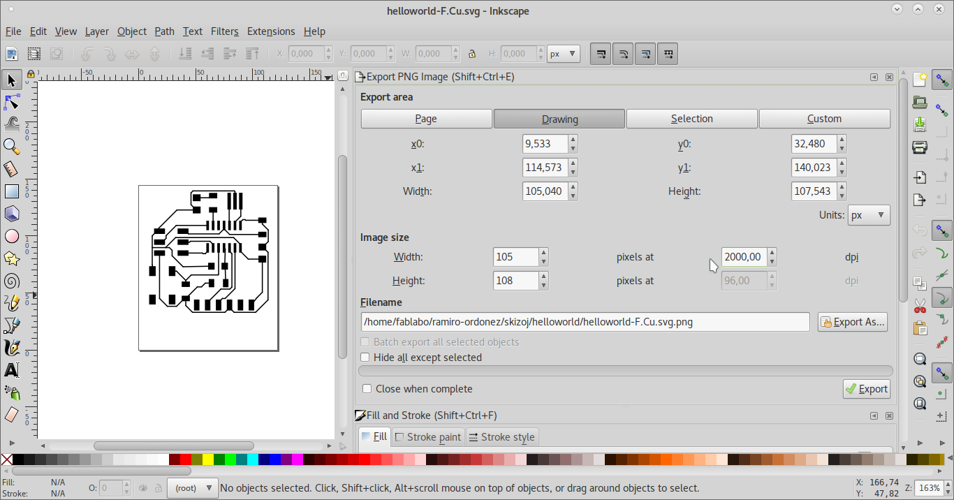
On Inkscape, the SVG of the copper layer is transformed to PNG.
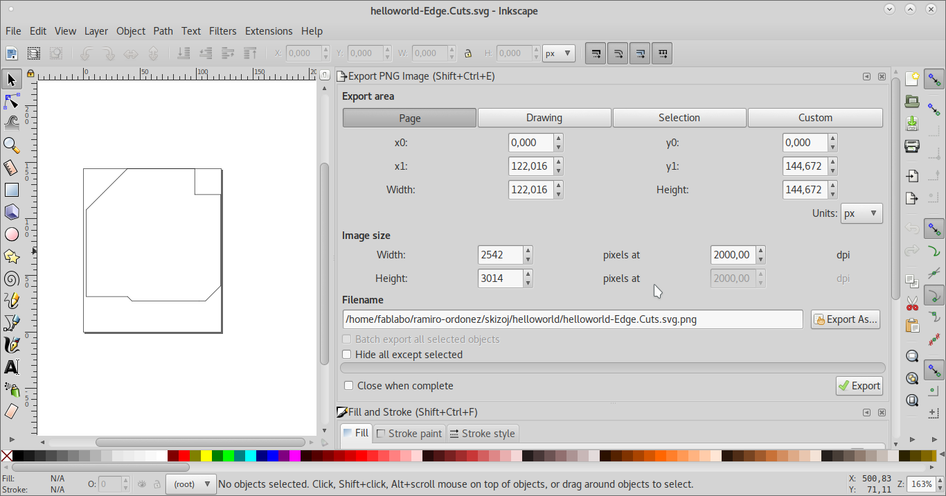
And the edge cuts layer is also transformed to PNG.
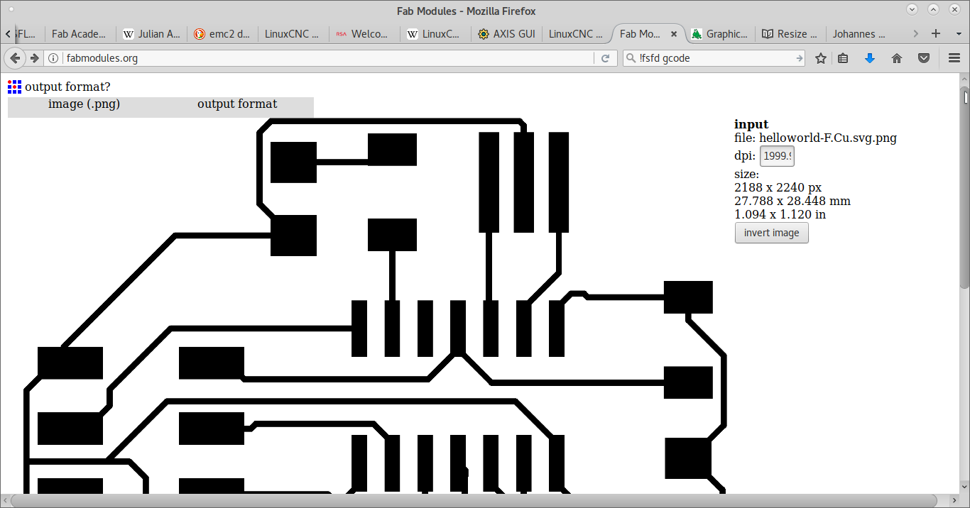
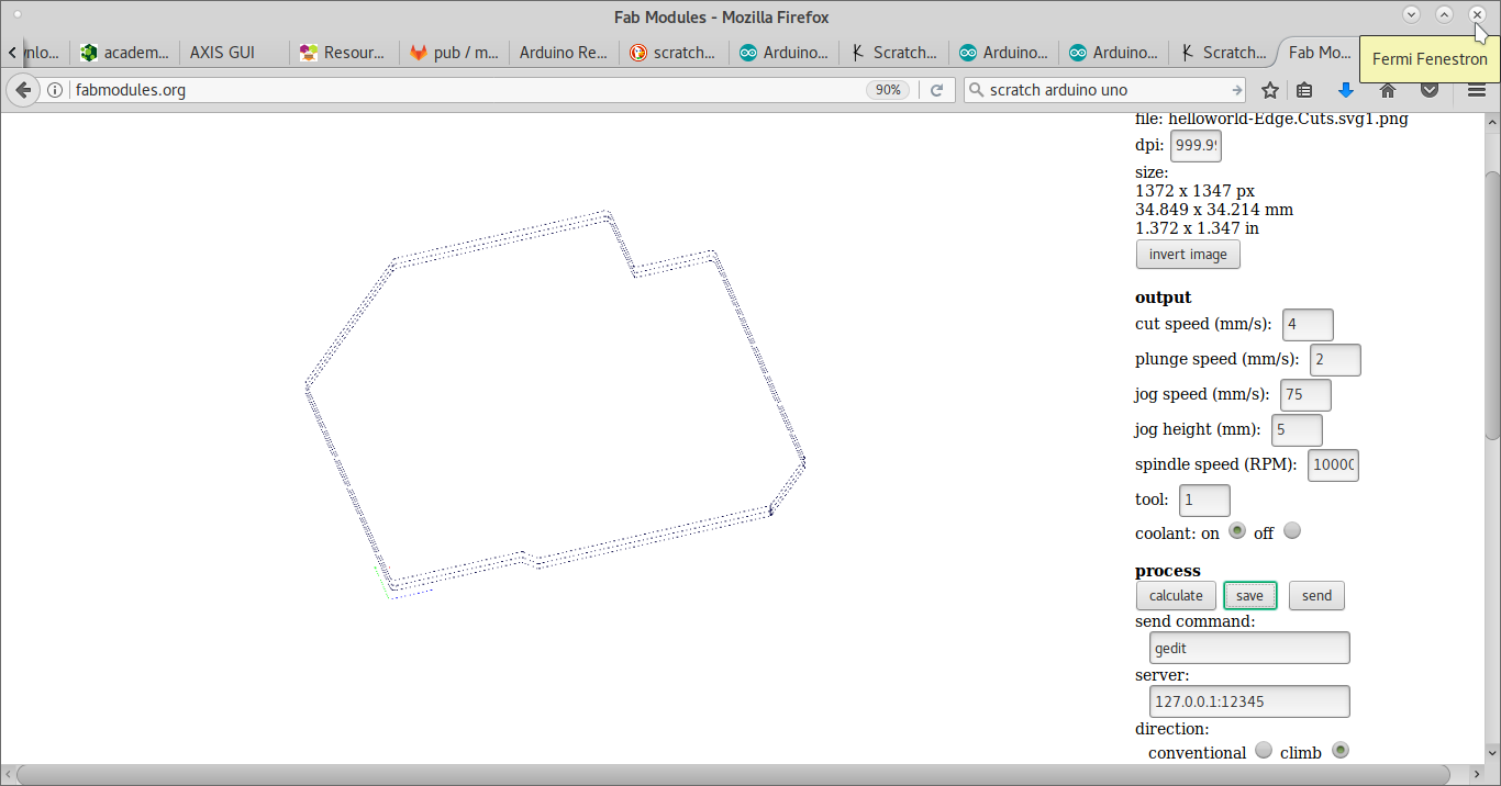
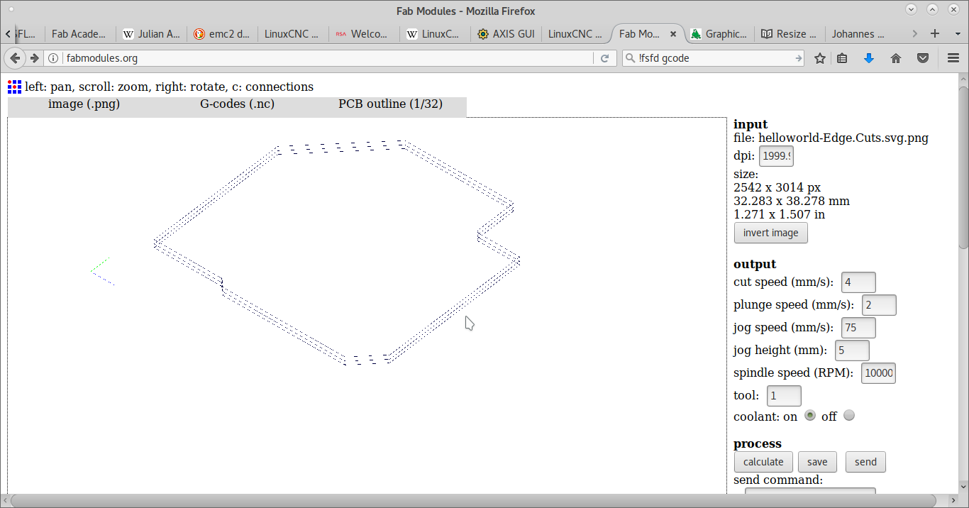
The PNG file of the PCB's copper layer is fed to FabModules.
These are two files of the rendering of Gcode generated for the edge cuts layer.
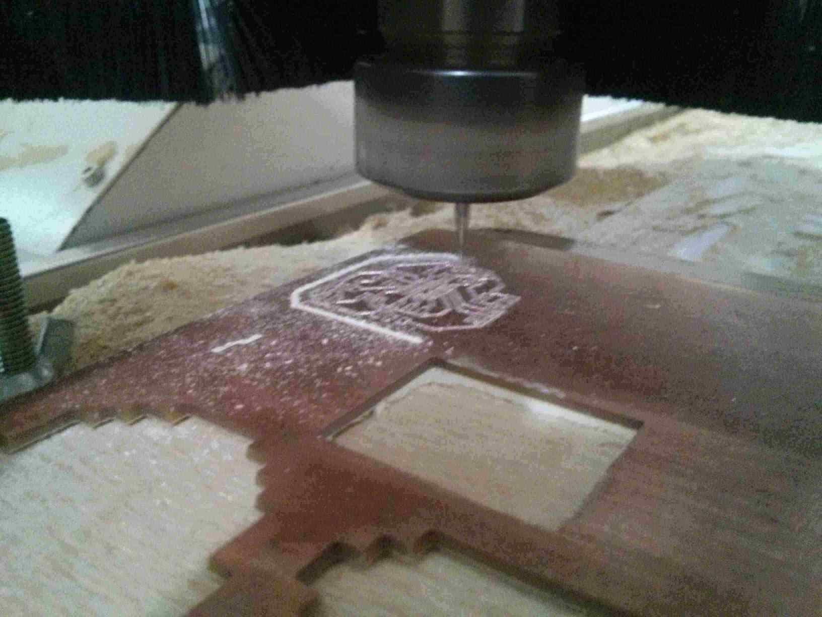
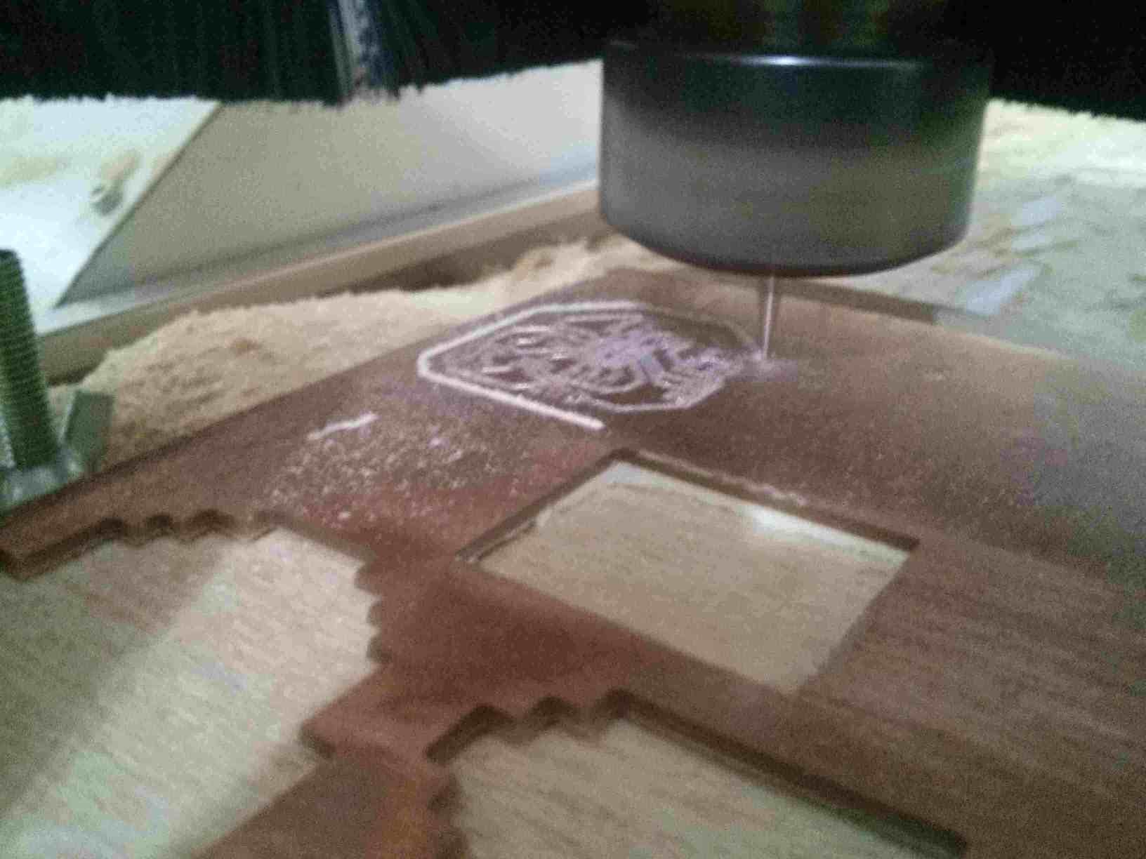
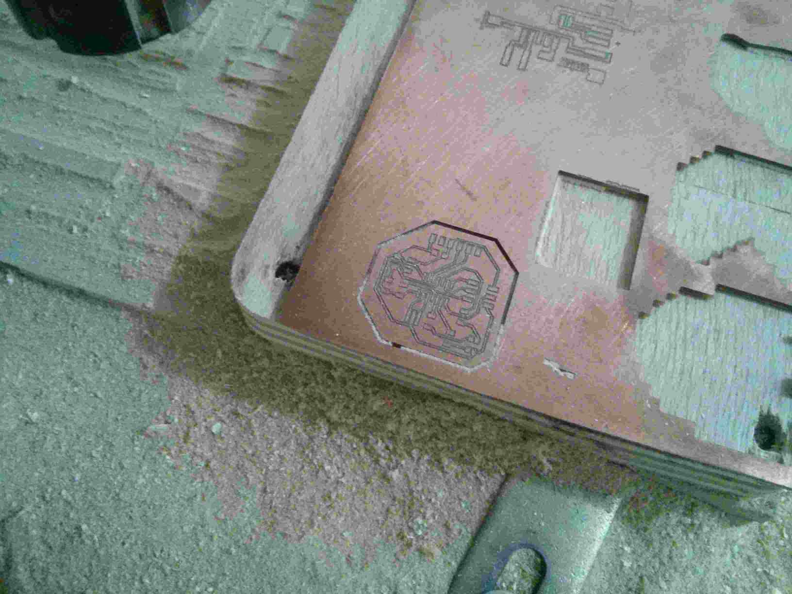
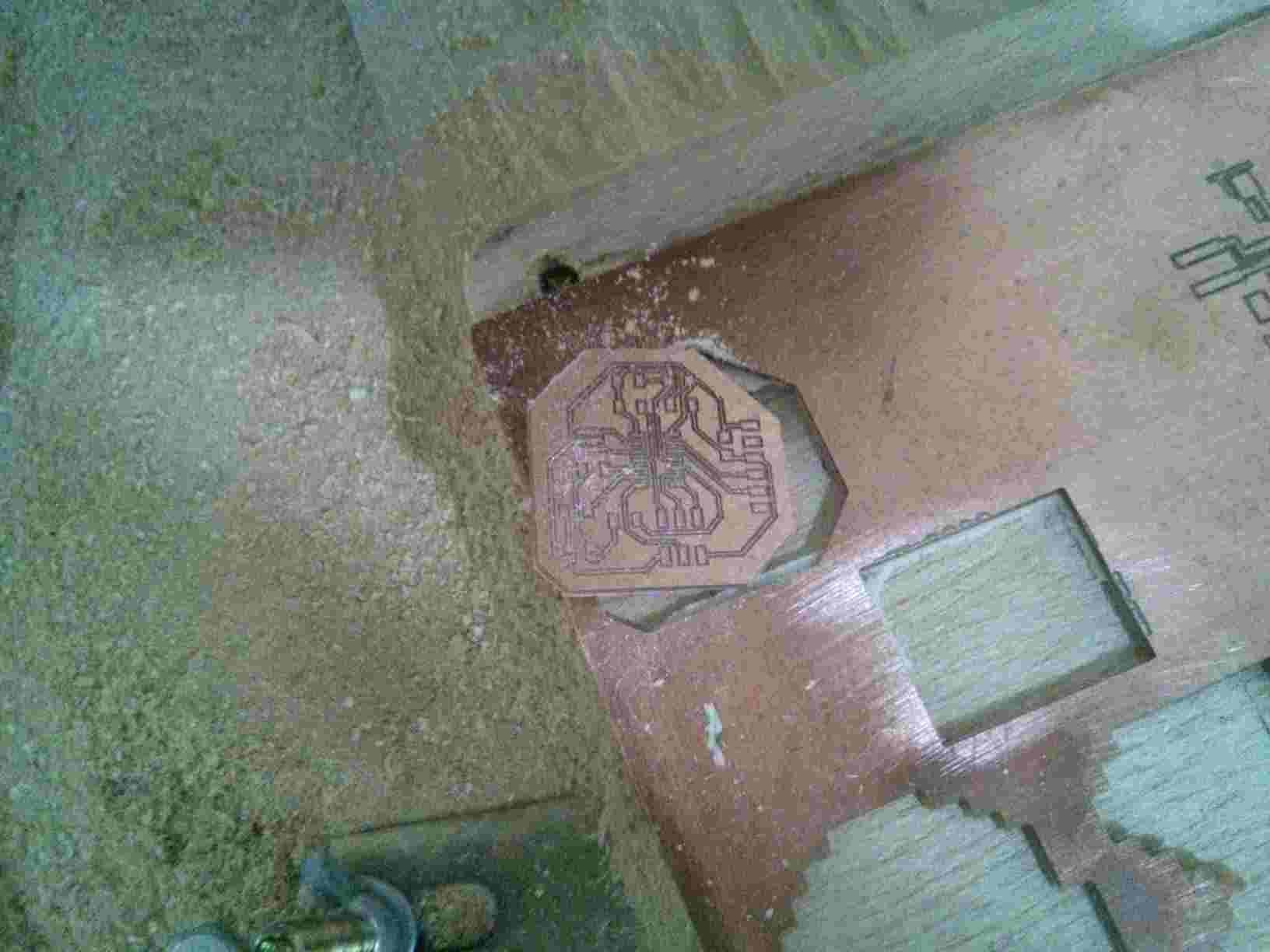
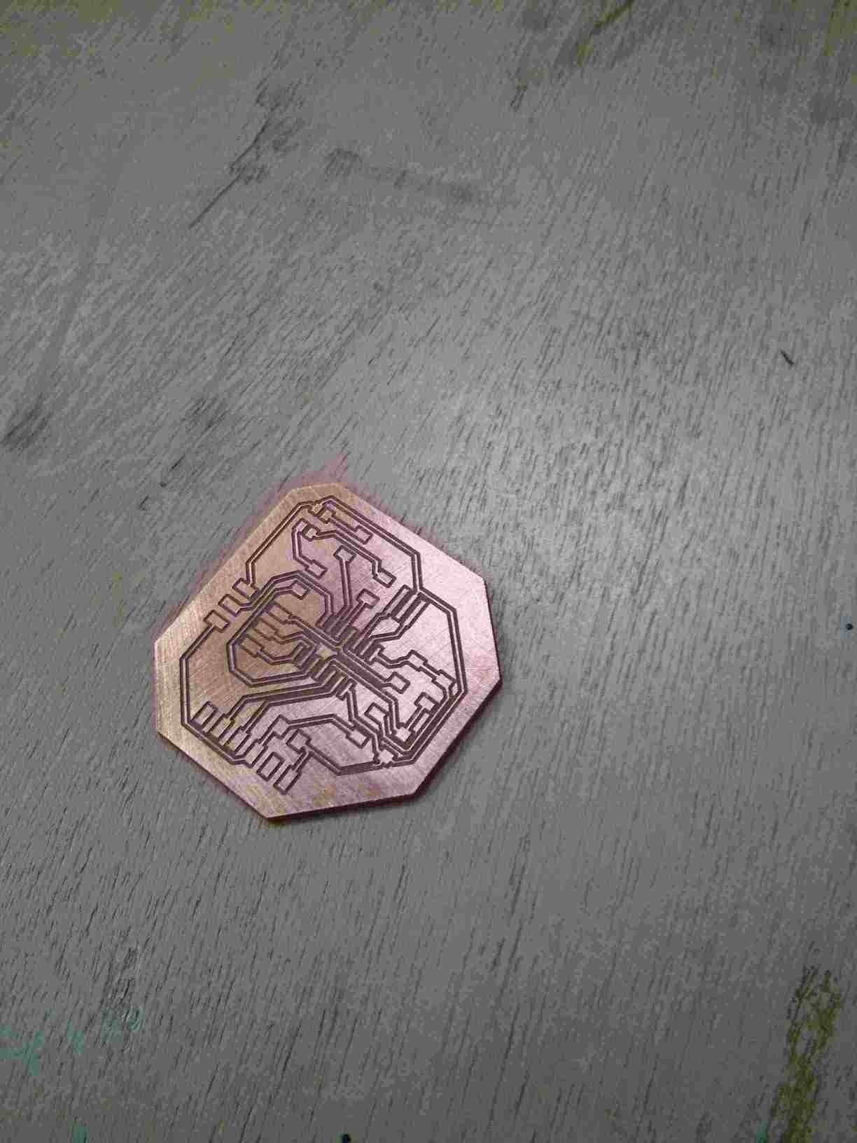
The PCB was milled with a smaller size. Probably it was made in mm and LinuxCNC detected it as inches. Now I know there is a Gcode to define this. But then I did not. This is the picture of the failed trace milling.
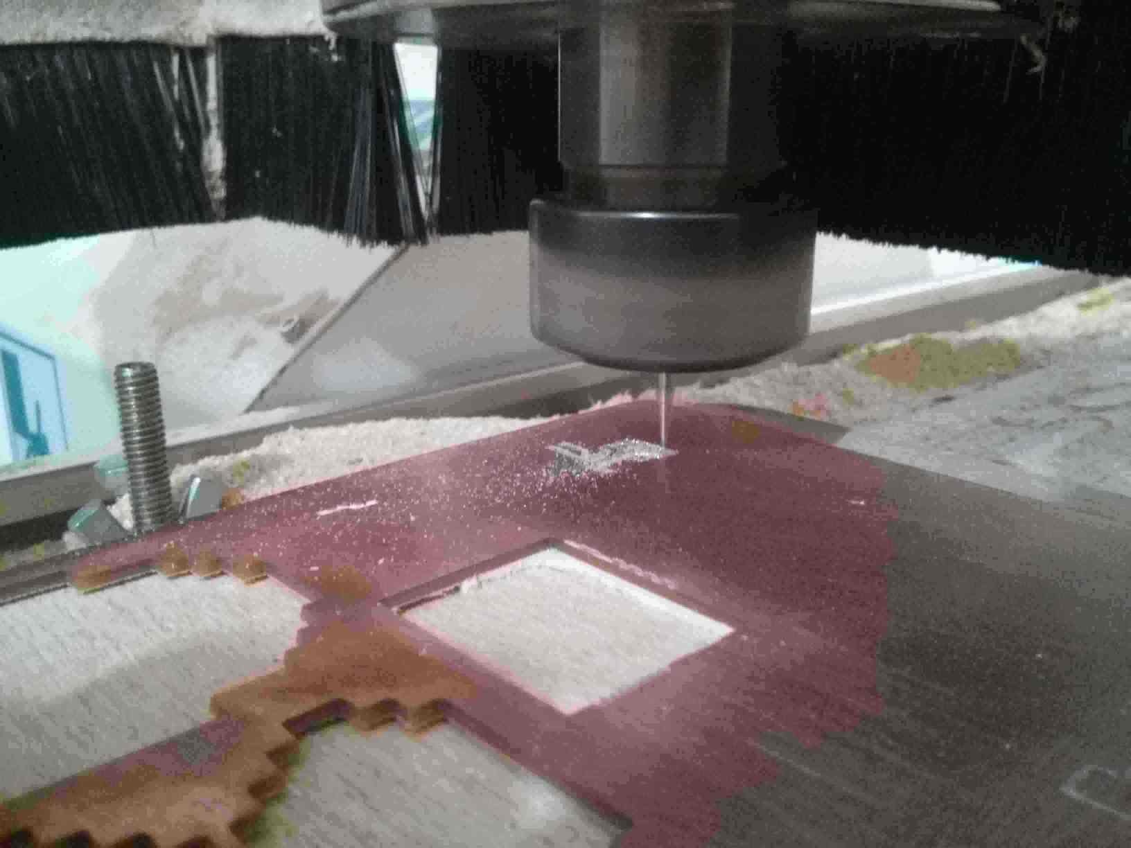
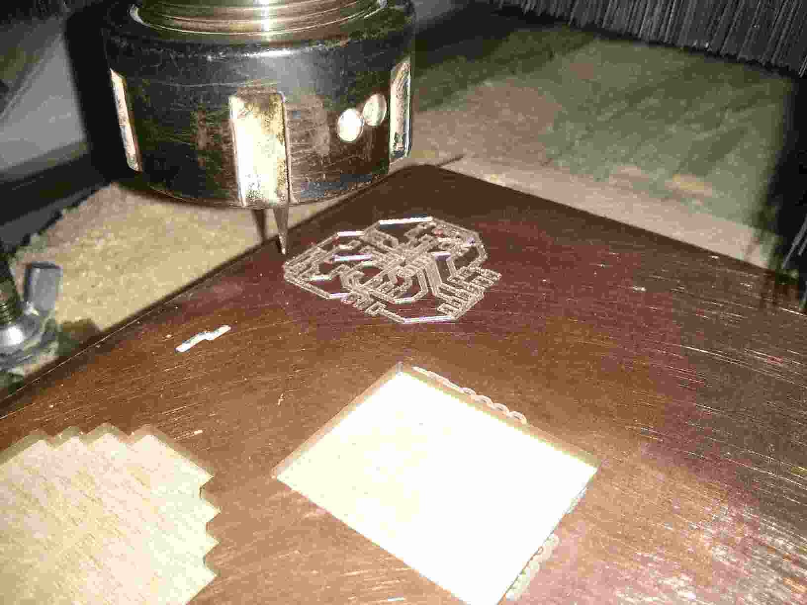
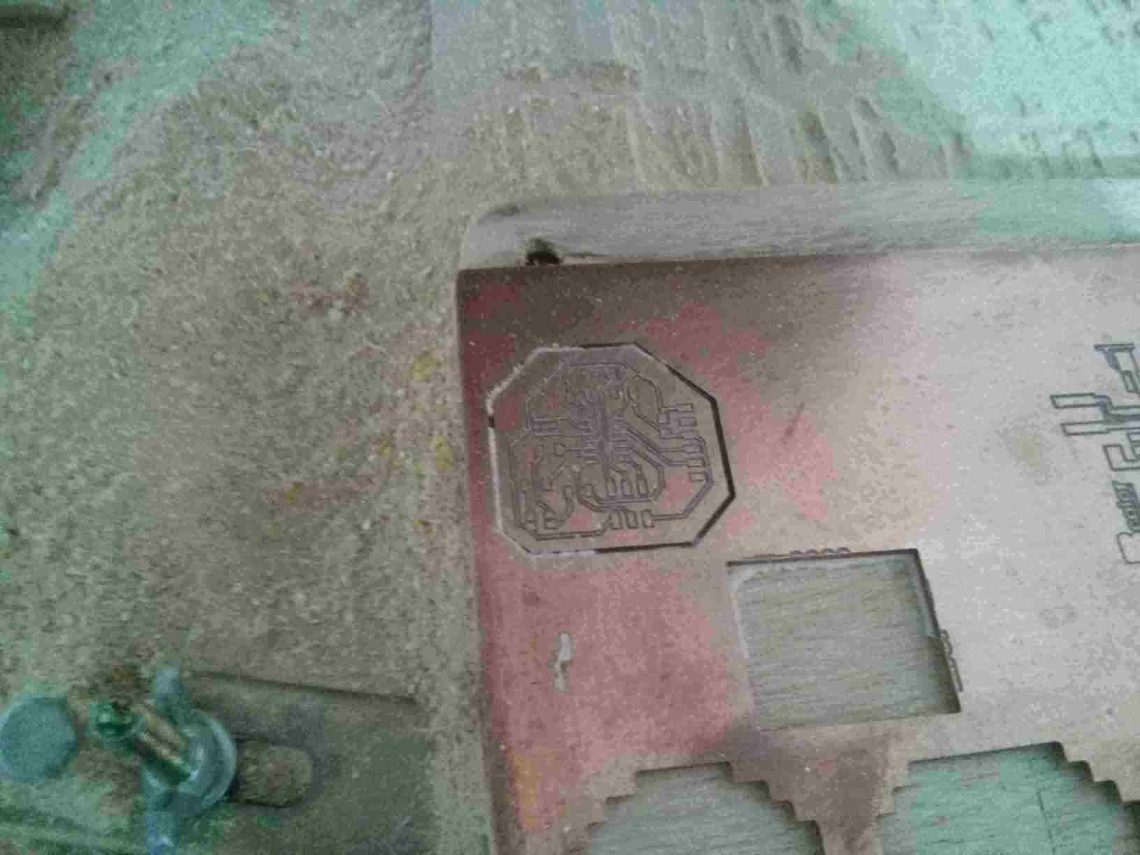
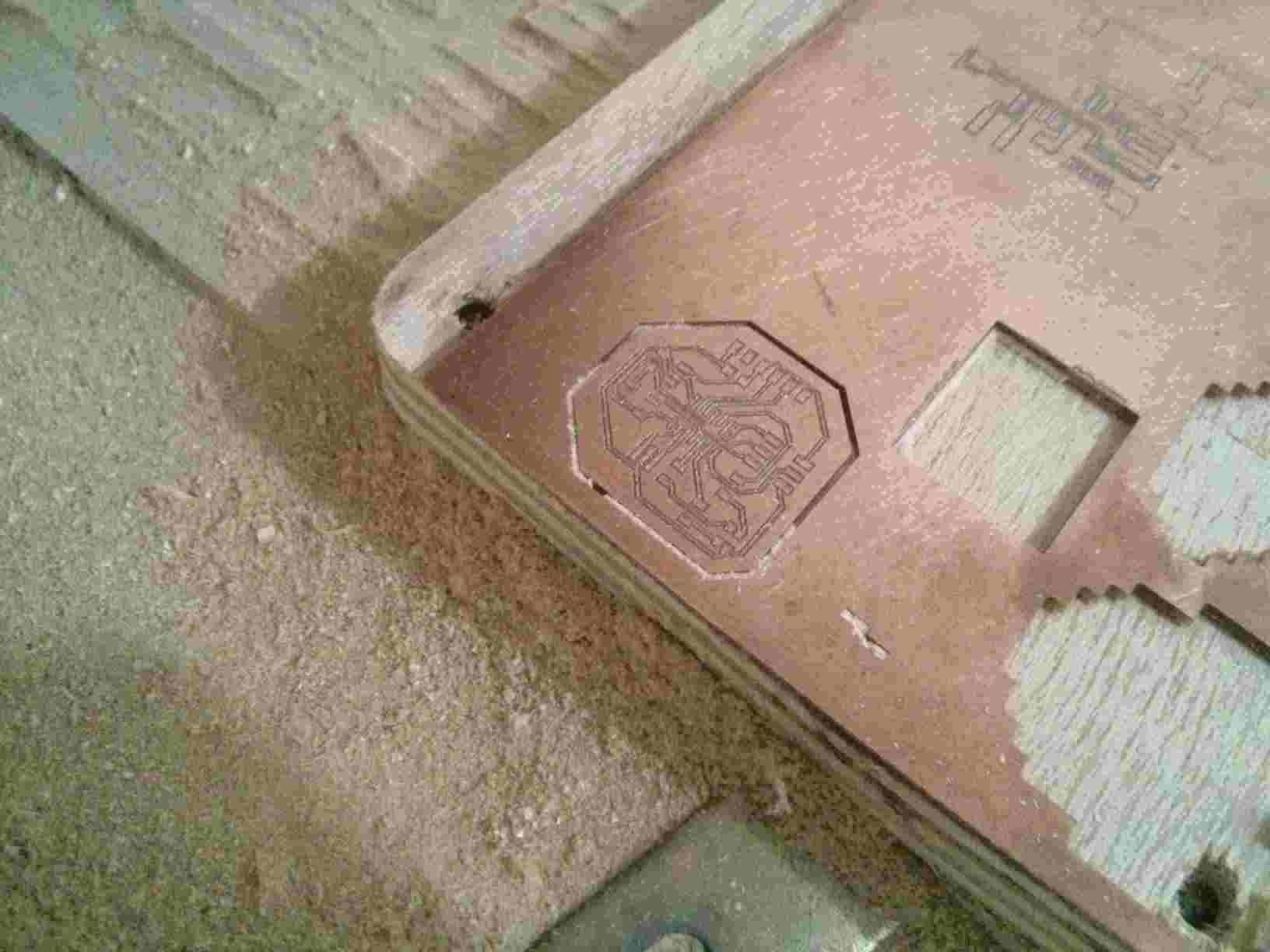
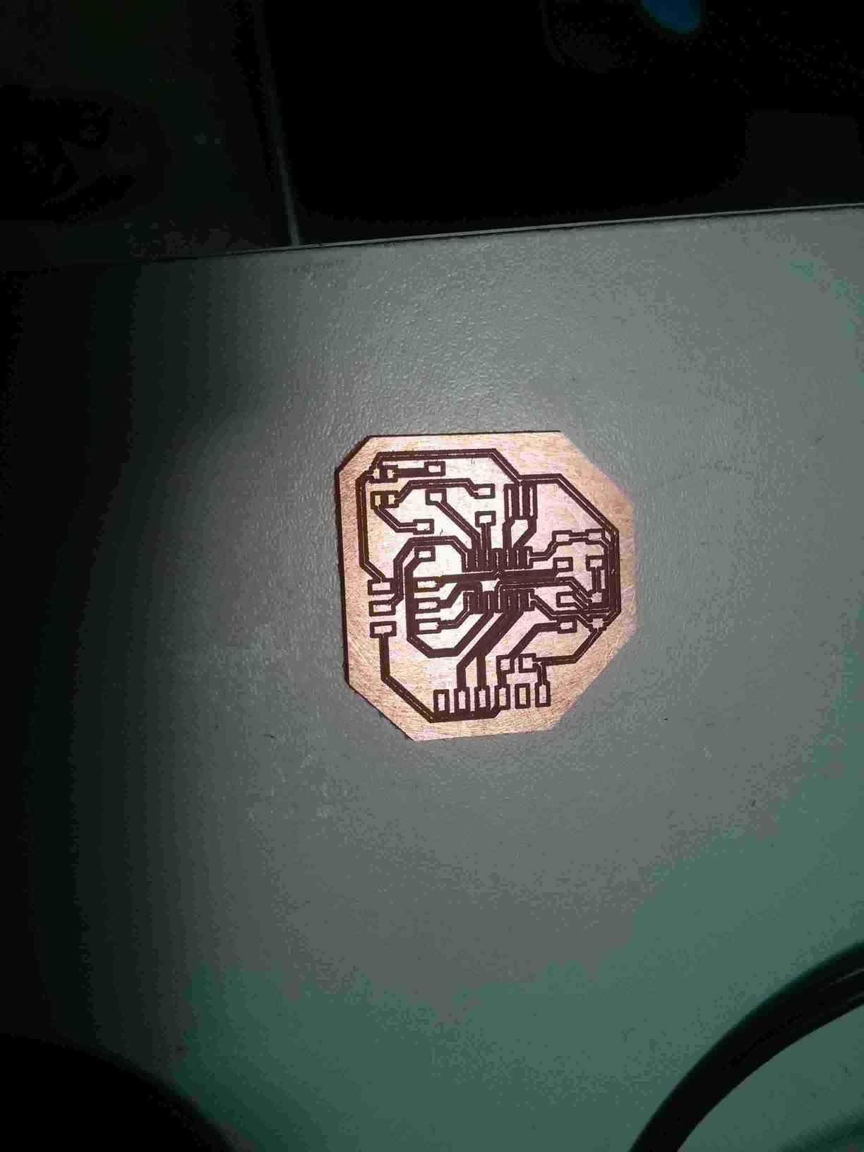
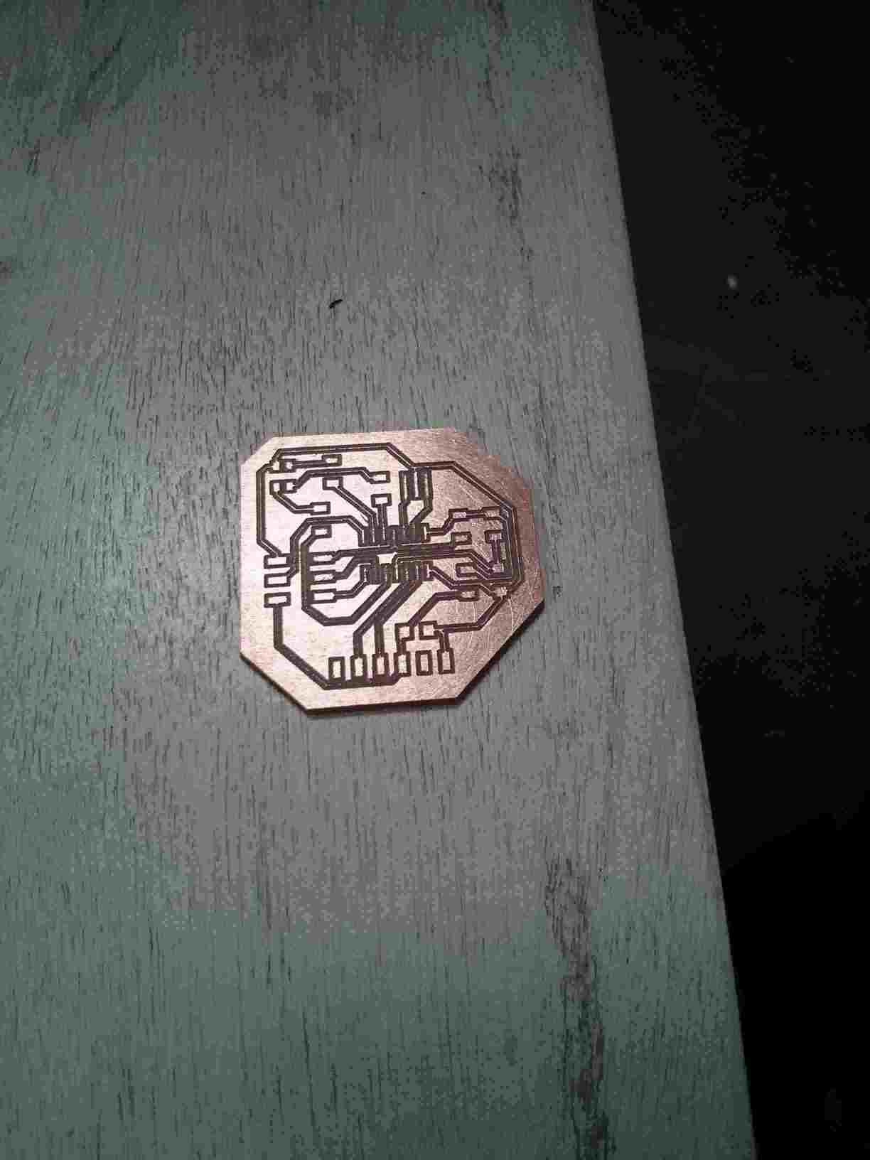
The corrected Gcode is fed to the CNC router. It finally cut a nice board. Of course I made about 10 failed millings before that.

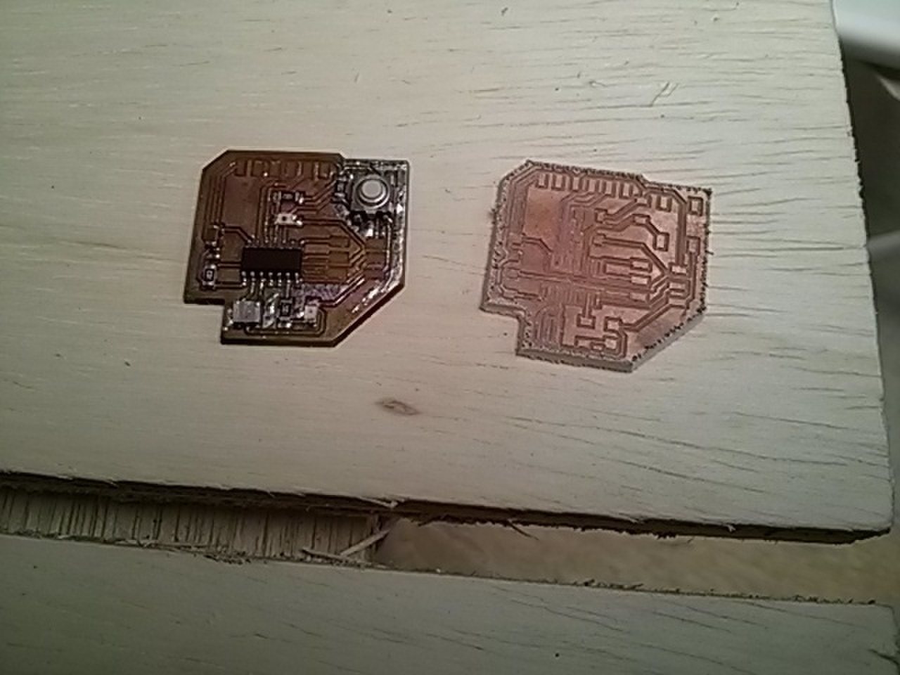
The first picture below is of two Printed Circuit Boards (PCBs):
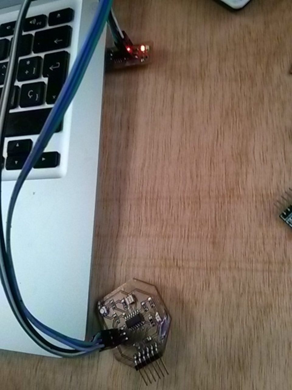
The next picture below is of the new PCB (with correct LED polarization; anode common). It is connected to the computer through the In-System Programmer (ISP).
The milling bit must be in mint condition in order to make thin traces. Otherwise the traces break when sanding.
KiCAD is capable of using Git libraries. It can even use Eagle libraries. This way it is possible to keep up-to-date without effort.
Making traces should be very easy with the automatic placing and tracing tools. I was not able to use it. But I look forward to taking the time to do it next time I design a board. If it will not make the best path automatically as well as manual (like I was told), I think it could be fairly trivial to make an algorithm that does. Time will tell.
Making KiCAD more user-friendly looks like a task for a graphic designer. I do not think I am a capable volunteer. But I can look for someone that is. I hope I can find someone.
BUG IN KiCAD MANUAL ==> Getting Started in KiCAD. Please change:
Click on the little circle at the end of pin 7 of the micro-controller and then click on the little circle on pin 2 of the LED. You can zoom in while you are placing the connection.
to
Click on the little circle at the end of pin 7 of the micro-controller and then click on the little circle on pin 1 of the LED. You can zoom in while you are placing the connection.
Using plugins


