Group Project
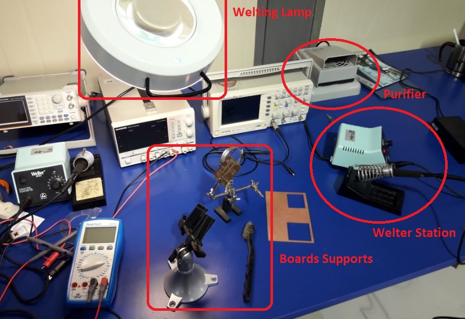
In the laboratory we have multimeters, osciloscope, welter, etc. I'll detal each equipment that can help to test our boards. Next,´we will analize all the equipment and how to apply to the activities
MULTIMETER
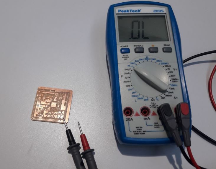
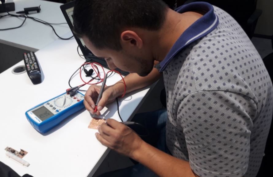
It is a measuring instrument that offers the possibility of measuring different electrical parameters and magnitudes in the same device. The most common are those of voltmeter, ammeter and ohmmeter. It is frequently used by personnel in the entire range of electronics and electricity.
I used the multimeter to confirm the ways of the board, also I can verify the connectivity of the board, measure values (resistor, voltage, current, etc)
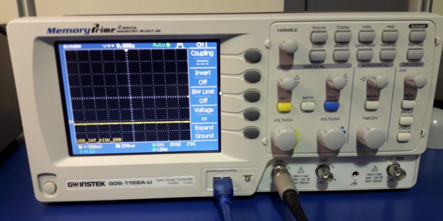
OSCILOSCOPE
The oscilloscope is basically a device that allows the graphic visualization of variable electrical signals over time. For this purpose, the oscilloscope has a screen in which the graph of the electrical signal applied as a function of time appears. The vertical axis (Y axis) represents the voltage of the signal; while the horizontal axis (X axis) represents time.
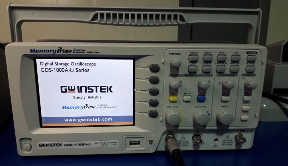
An oscilloscope can measure a multitude of physical quantities, it simply needs the appropriate probe that converts the quantity to be measured into an electrical signal (eg in the case of sound, a microphone converts the acoustic signal into an electrical signal).
Due to the diversity of measurements and magnitudes that can be studied with oscilloscopes, these are used in very different fields ranging from medicine to automotive mechanics.
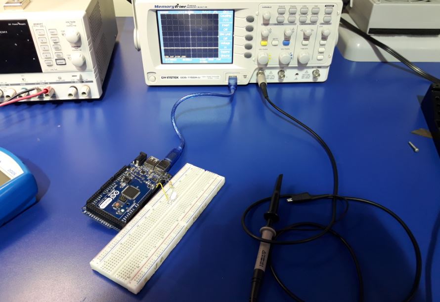
I used the oscilloscope to verify the PWM signal applied to the LED using an Arduino MEGA
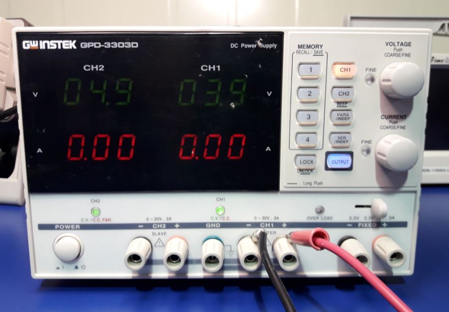
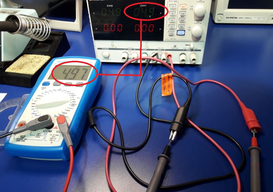
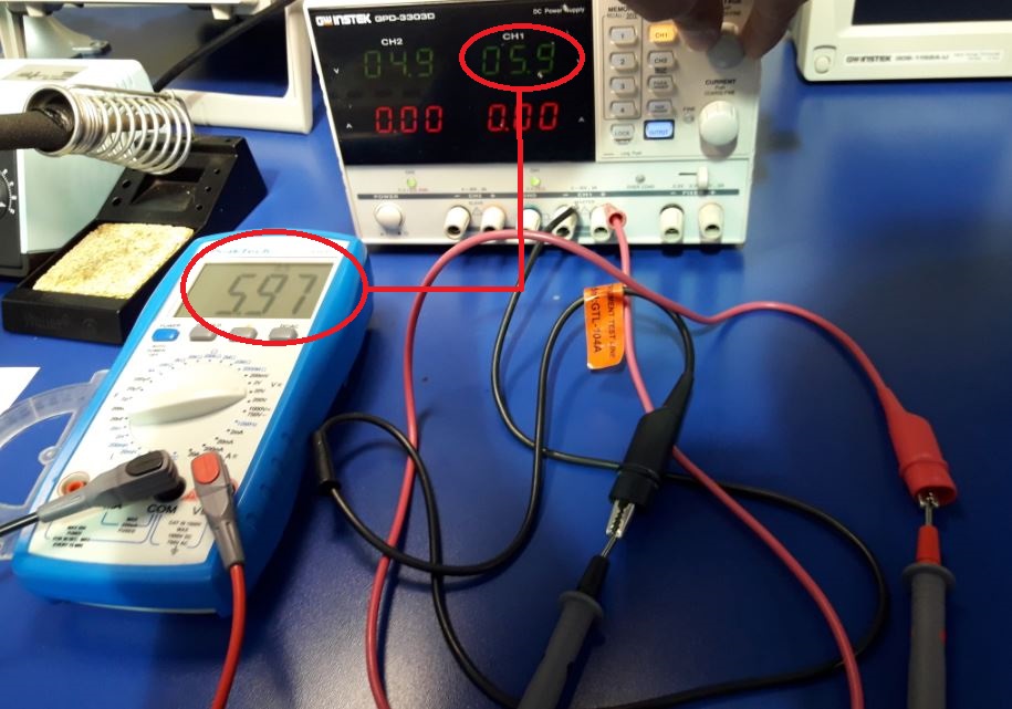
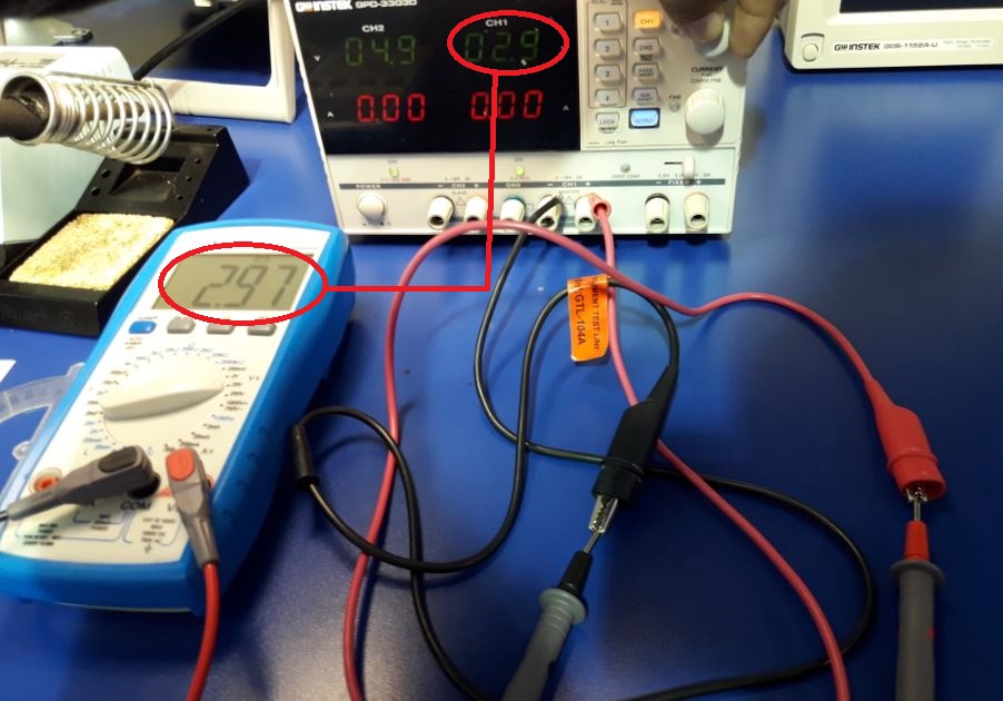
POWER SUPPLY
It is an electronic circuit that transforms electrical input power, either direct current or alternating current, into an electrical power output, both direct current and alternating current, with a voltage level or current or both simultaneously in a constant.
To verify the power source I used a Multimeter to check the measures of the output signals
OTHER INSTRUMENTS
All the tutorial videos were sponsored by SparkFun Electronics
Below, From my point of view I present ten useful rules that must be taken into account or practiced by electronics designers when designing PCB boards for commercial manufacturing using design software. They are not in chronological order or assigned a level of specific importance, but, taken together, they make a big difference for any design.
Rule 1: use the appropriate grid. Find a grid whose spaces adapt to the amount of components you will use and take advantage of the entire space. Although the idea of using several grids may seem appealing, a bit of additional reflection in the initial design phase can avoid space-related difficulties and allow you to make the most of the plate. Take advantage of the fact that many devices are available in various sizes. Also, since the polygon is an important way to add copper to the plate, and plates with multiple grids often produce discrepancies in the way the polygon is filled, the use of more than one grid can make the life more difficult than necessary.
Rule 2: the clues should be as short and direct as possible. It sounds simple and obvious, but remember this rule at all times, even if the result is that you must correct the distribution of part of the plate to optimize the length of the tracks. This applies in particular to high-speed analog and digital circuits in which impedance and parasitic effects can limit the performance of the system.
Rule 3: As far as possible, use a plan to manage the distribution of the lines and ground connections. Filling the drawing is a quick and easy option in most PCB design software. It applies enough copper to the common connections and really helps to ensure that the energy flows as effectively as possible with minimum impedance or voltage drop and that the returns from the ground connections are adequate. If possible, trace several power lines in the same area of the plate and remember that if the ground plane is traced in a very large section of a layer, it can have a positive impact on the feedback between the lines drawn on or in adjacent layers.
Rule 4: group the related components and the test points if you need them. For example, put the discrete components needed for an operational amplifier near the device so that the bypass capacitors and resistors are placed with it. This helps with the length of the tracks in Rule 2 and makes it easier to run tests and find bugs.
Rule 5: Create panels of your PCB by replicing it several times on a larger plate. By using the size that is best suited to the equipment used by the selected manufacturer, the cost of prototypes and manufacturing will be improved. Begin by distributing the plate as in a panel. Contact the manufacturer to acquire the preferred size specification for each panel. Then, when you have corrected the design rules, do your best to repeat your design several times in the preferred panel size.
Rule 6: consolidate the values of the components. As a designer, you will have selected some discrete components of greater or lesser value that work in the same way. Consolidating the components in a range of standard values makes the bill of materials simpler and probably cheaper. In addition, in the long term, decisions regarding the stock are facilitated if there is a variety of plates based on the preferred values of the devices.
Rule 7: Check the design rules as often as you can. The DRC function for this purpose in the PCB design software is not delayed, and if you check the rules often, you can save hours in much more complex designs and it's an excellent habit. All the decisions of the distribution of the plate are important, and checking the design rules constantly allows you to always keep in mind the most important thing.
Rule 8: use screen printing wisely. Screen printing can be used to communicate useful information to the person who builds the board, to the maintenance or testing engineers and even to the person who installs or operates the device. The clear labels of the functions and the test points are obvious, but the orientation of the components and connectors should also be taken into account as far as possible. The annotations are used even though they sometimes end up covered by the components after assembly. The use of screen printing on both sides of the plate can reduce the need for reconditioning and simplify production.
Rule 9: uncoupling the capacitors is not optional. Do not try to optimize your design by avoiding uncoupling the lines and relying on the absolute limits of the technical sheets of the components. The capacitors are economical and resistant. Take time to install them when possible, and remember Rule 6 about using a range of standard values so you do not have inventory problems.
Rule 10: Generate your own PCB fabrication data and verify it before sending the plates. Most license plate manufacturers do it directly from the download file, but if you enter your Gerber files first and review them using a free tool to make sure they look the way you expect them to look, you can avoid misunderstandings. In addition, you can even find errors without intending to before they are printed forever in fiberglass, resin and copper.
As circuit designs are shared more openly and more and more teams of designers depend on reference designs, we believe it is very important that these rules continue to be observed in the design of printed circuit boards. By maintaining control over the basics, designers also maintain the flexibility to add value to their products and make the most of each plate they design. Finally, anyone who just begins in the design of plates will learn much more quickly and achieve higher confidence levels if they always remember the basic rules.
Individual Project (FIRST EXAMPLE)
To start with this week's activities, I'm going to design an electronic circuit shown in this link but with some modification to use some software to design, adding a button and a led, and using Atmega328p au to complete the asignment

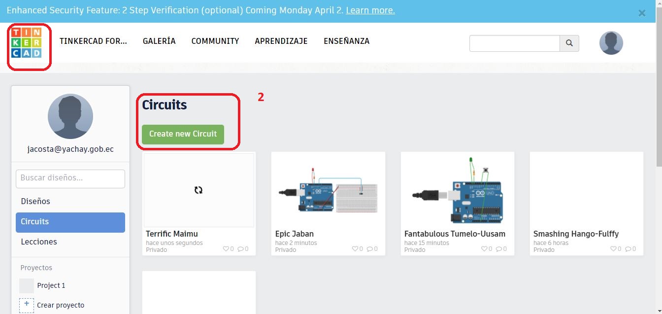
I'm going to start designing the board using Circuits.IO, it is a free online software to design electronic circuits, you can access to the plataformby clicking here
.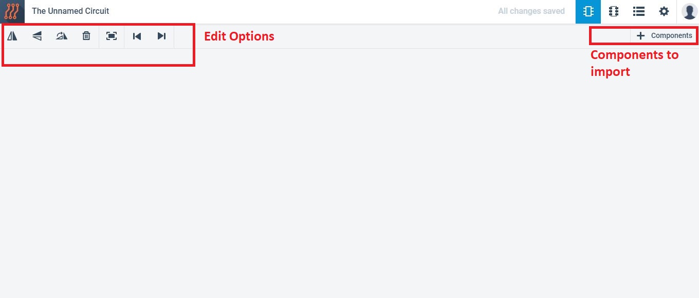
Once in the webpage, let's create a circuit, so click in components tag, then a window will be displayed below. Check the picture
.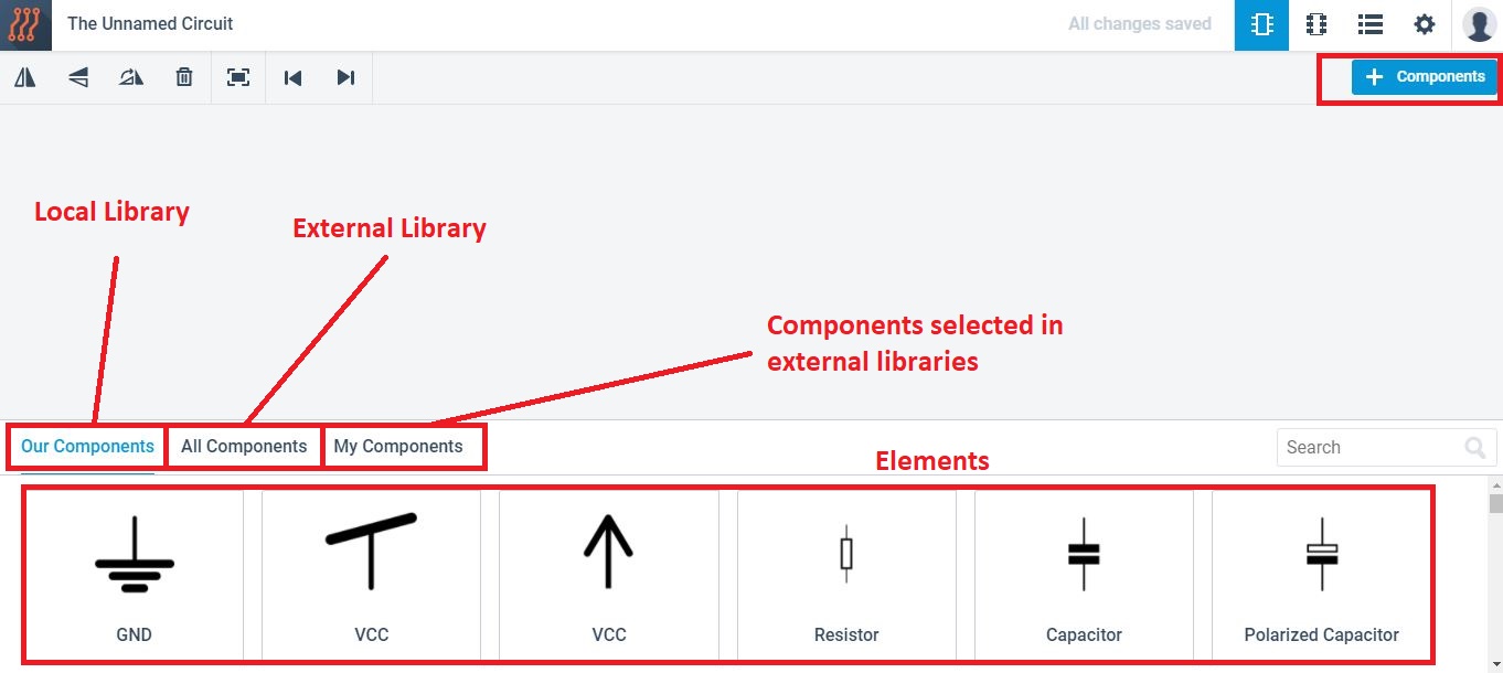
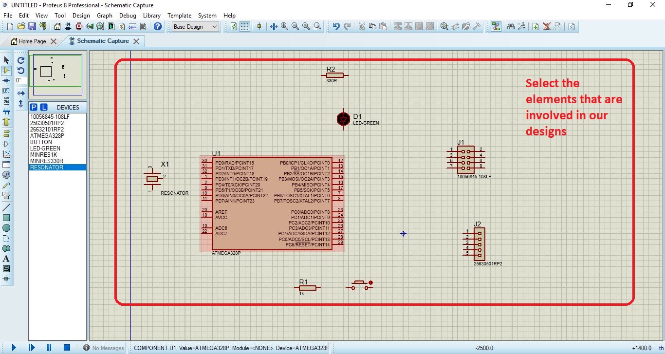
To start designing I need to select all the parts involved on the activity, so I will use:
According the design made I will start my own design, let's find the elements and put them on the workspace.
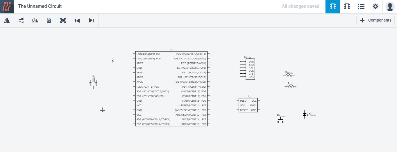
Then Ill use virtual wires to connect the circuit.
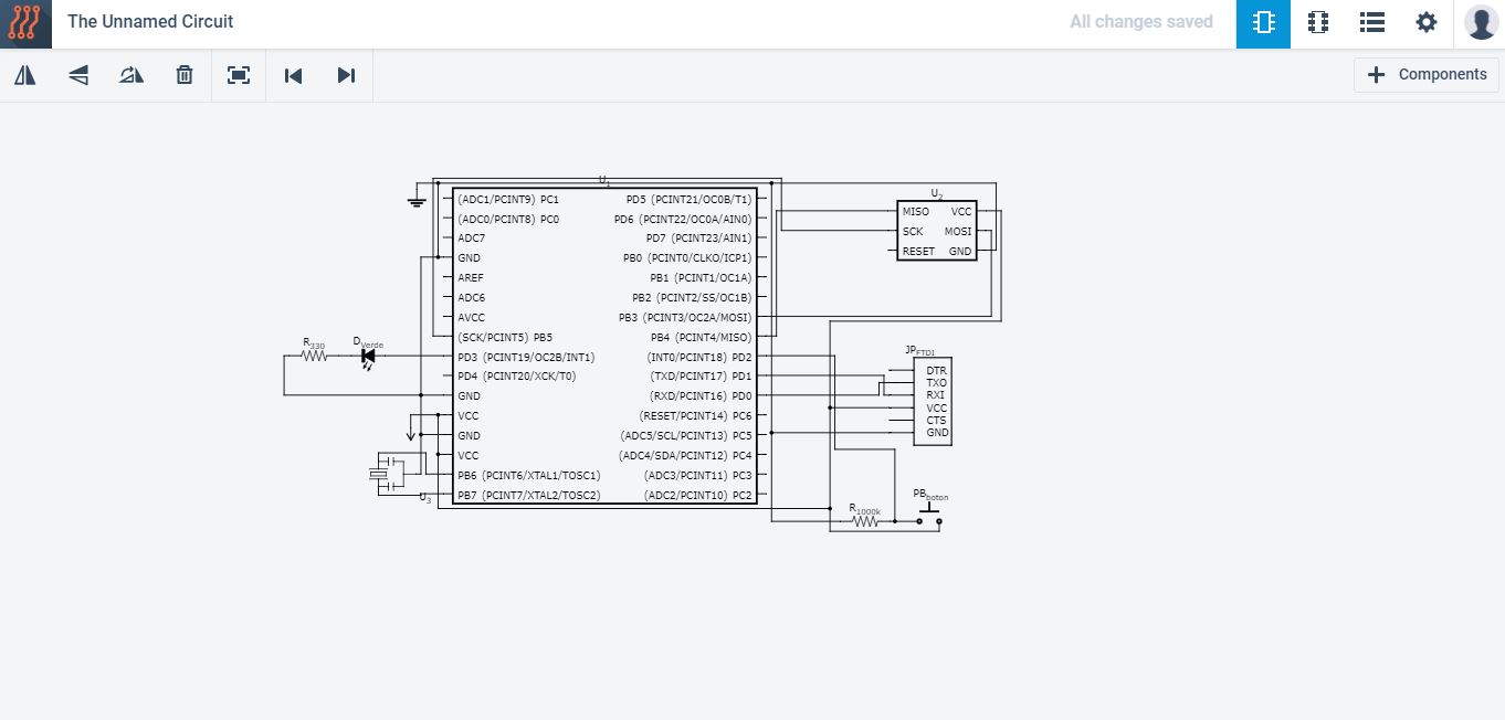
Then, I will start designing the PCB circuit
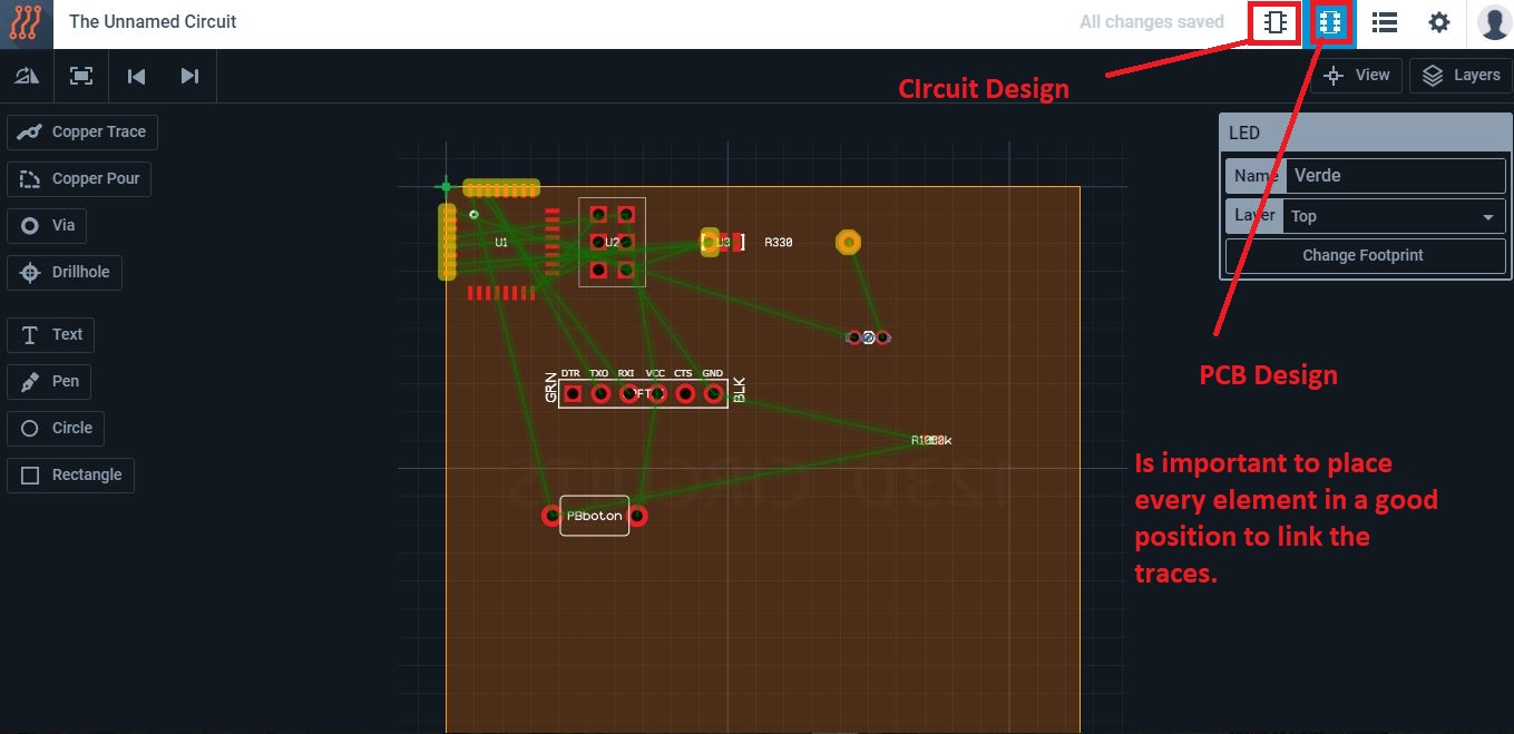
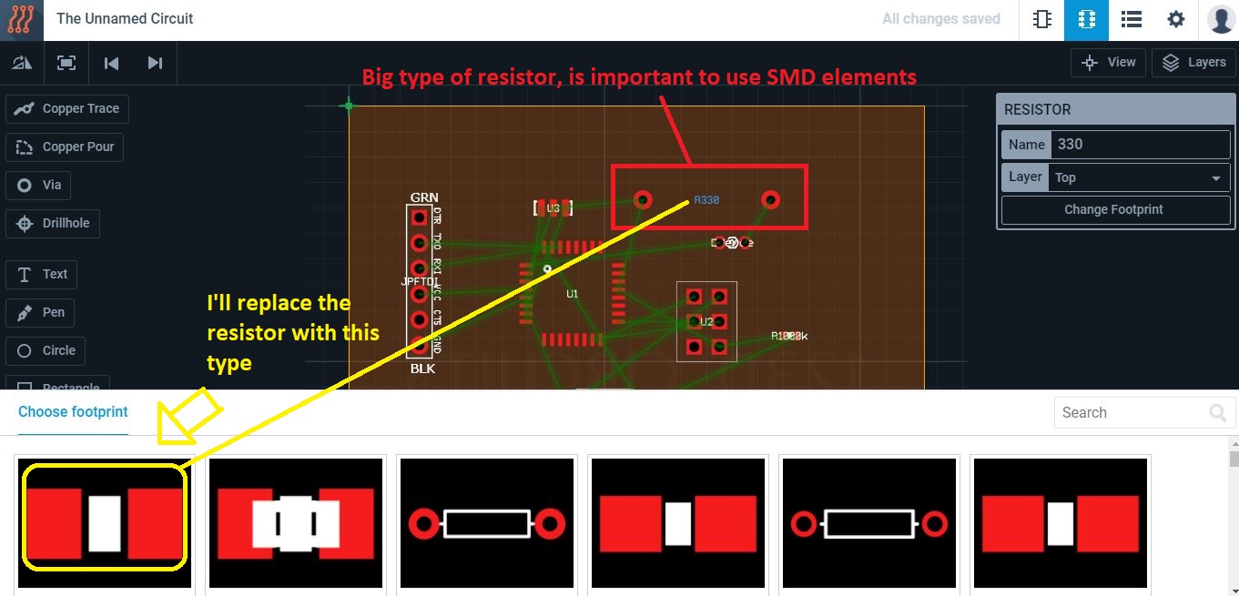
When click on each element, is posible to change their model and type to fit in the board
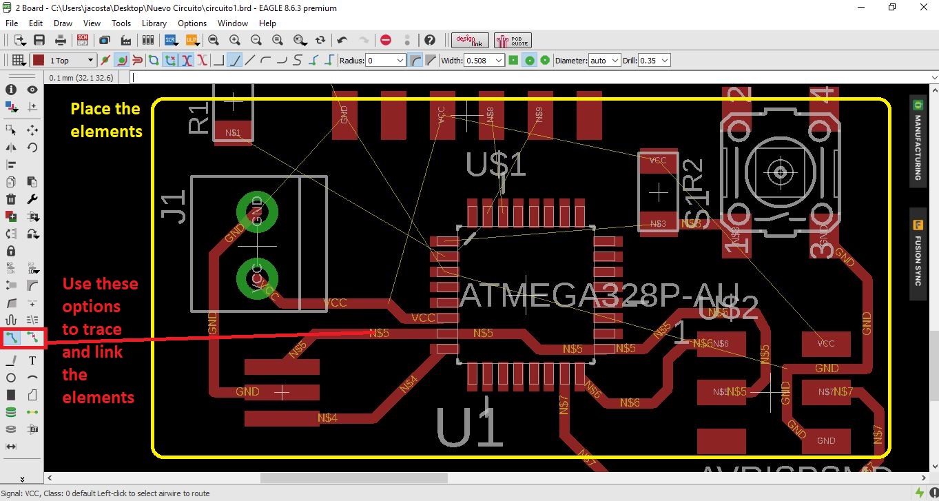
Then I will trace the elements
Finally, i will locate the elements to take advantage of every element place to reduce the dimension of my board.
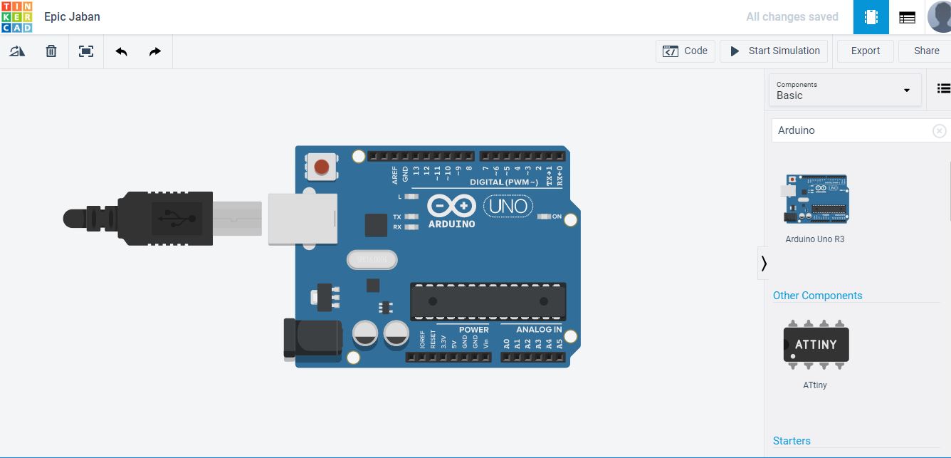
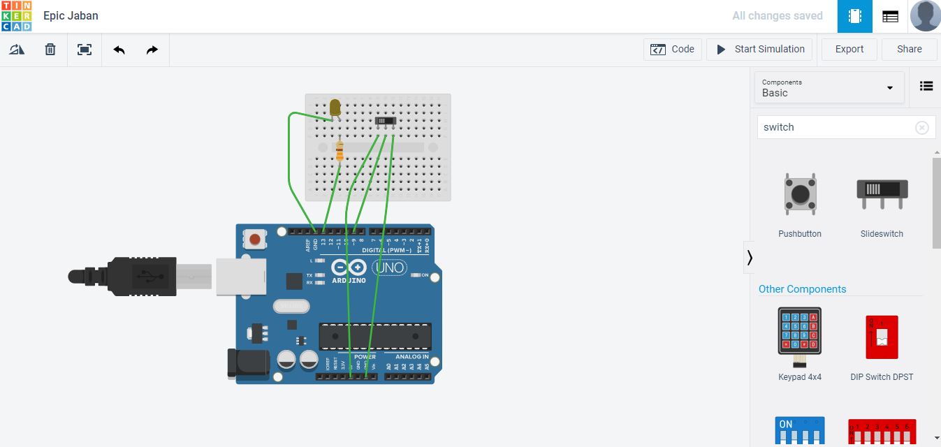
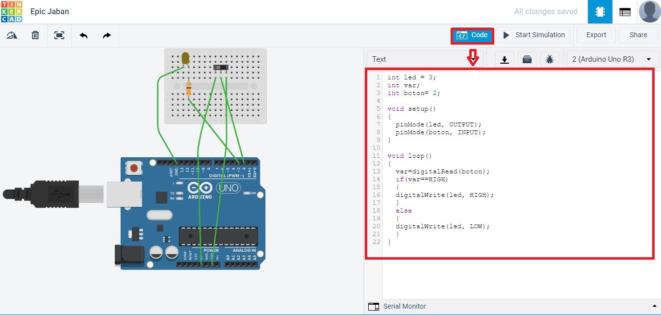
It's important to verify the functionability, so I will use TinkerCAD to design a simulation of the board, in this case i will use an Arduino Uno who has an Atmega 328p AU integrated, I identify the pins of the board by checking a datasheet of the microcontrolers. To simulate your boards you can export from circuits.io to TinkerCAD, more information, here
Then create and configure the space to work
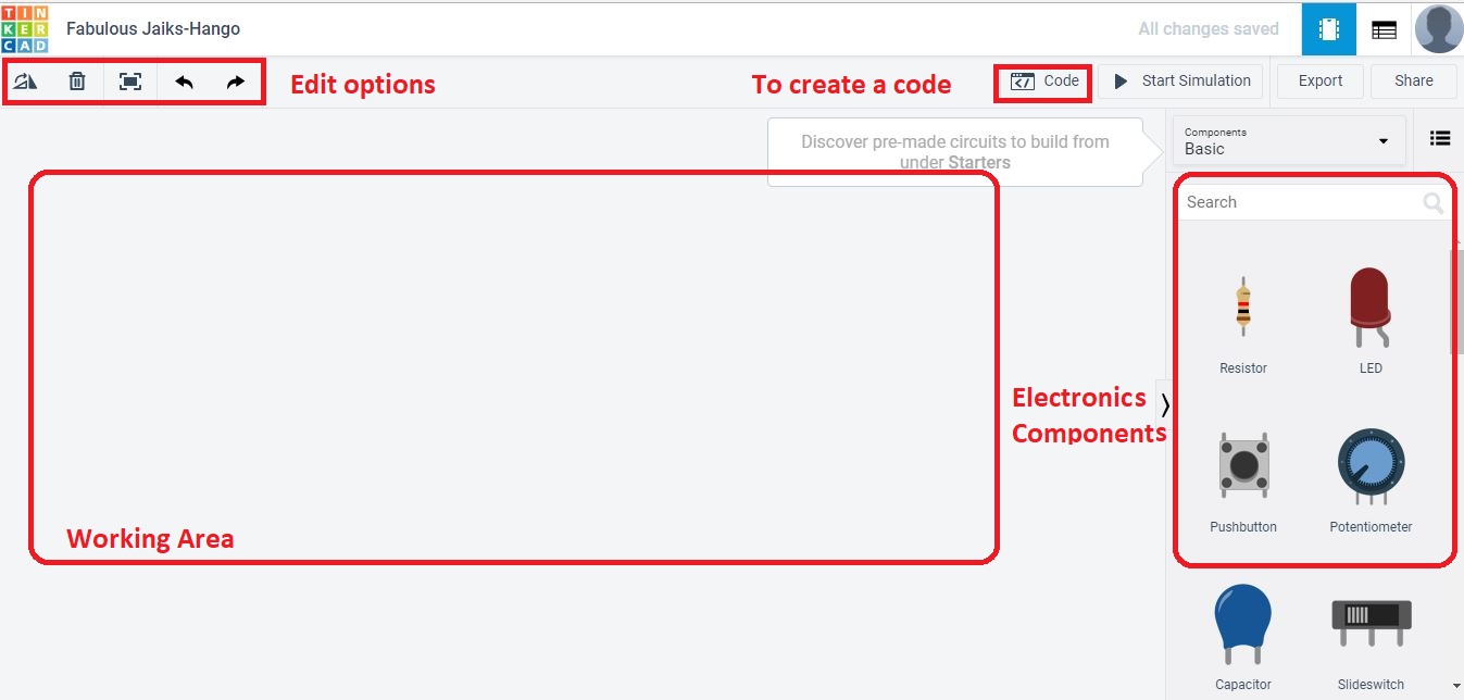
I started searching the elements in the elements bar, and then correcting problems
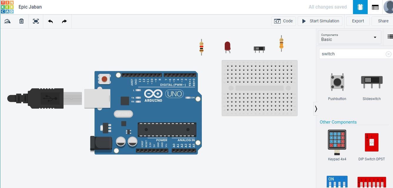
Then I will use the virtual wires to connect the elements as I show
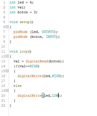
Then is important to program the board, to do this I used
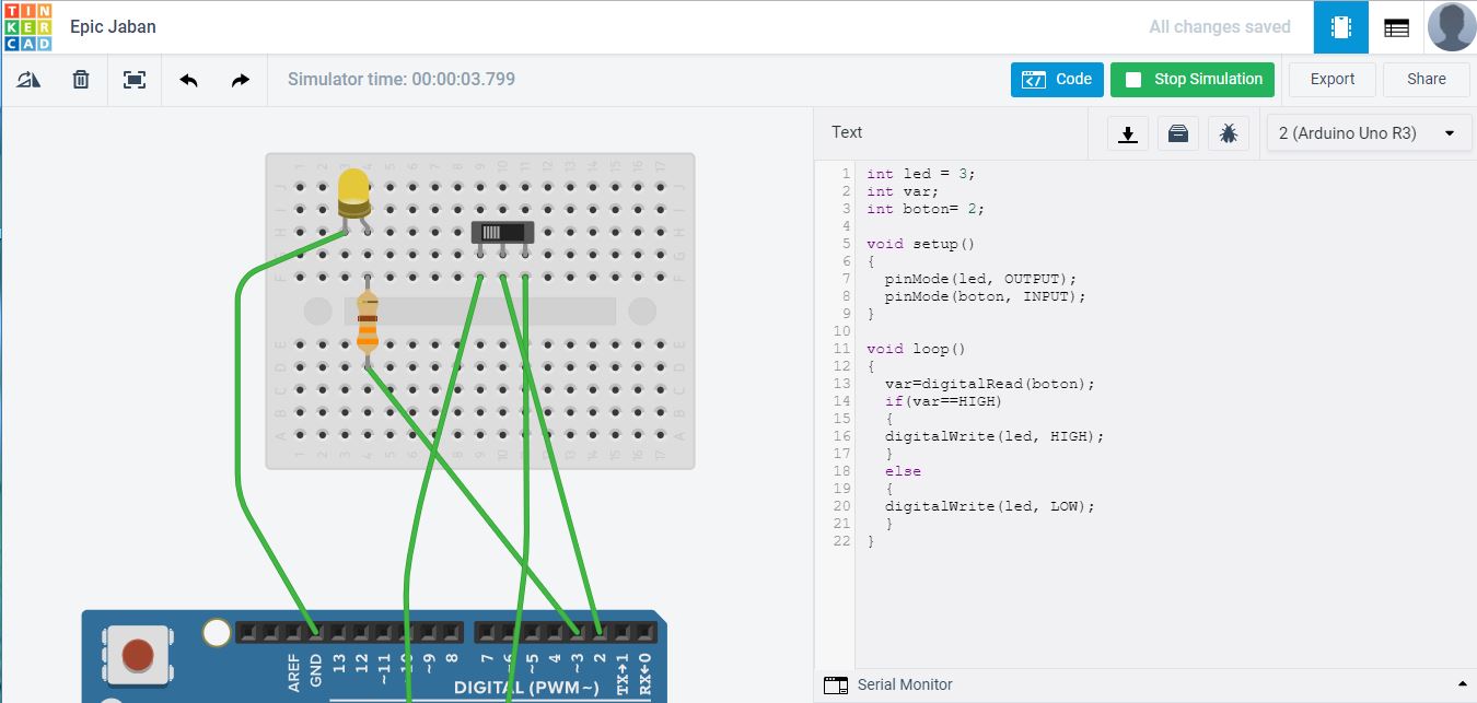
Then I will run to verify the functionability
As an extra and helpful material, I share the Atmega328p PinOut click here
The design now is clear, but the problem is the software not to allow me to download the diagram for fabricating, for this reason I have designed the same circuit on proteus and eagle
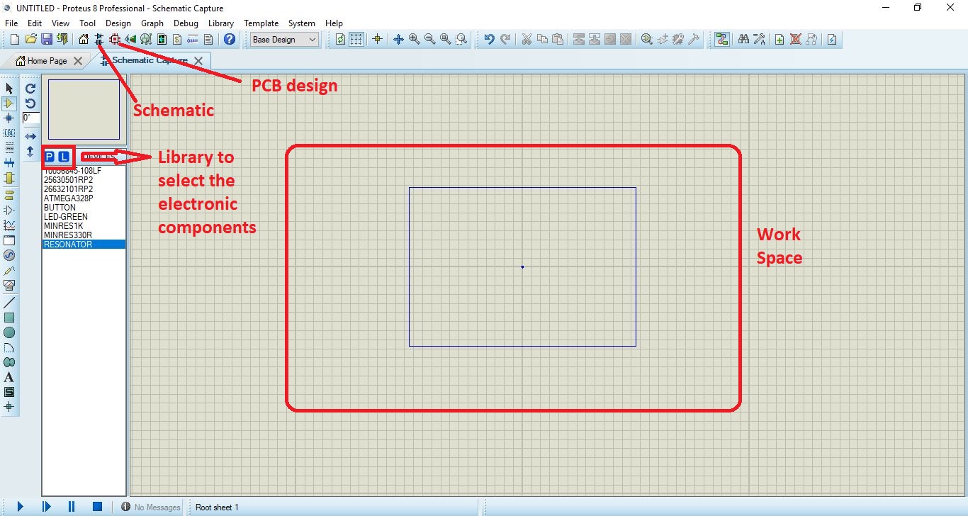
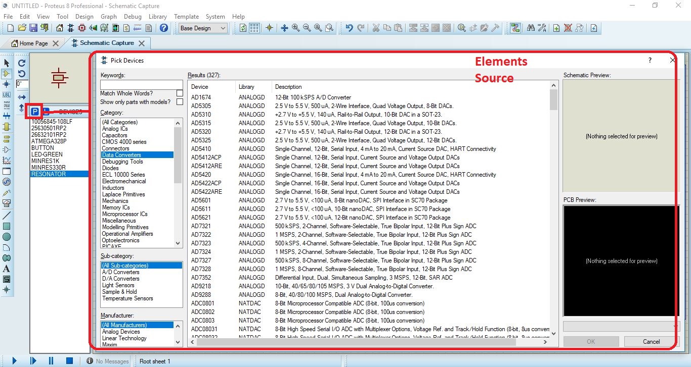
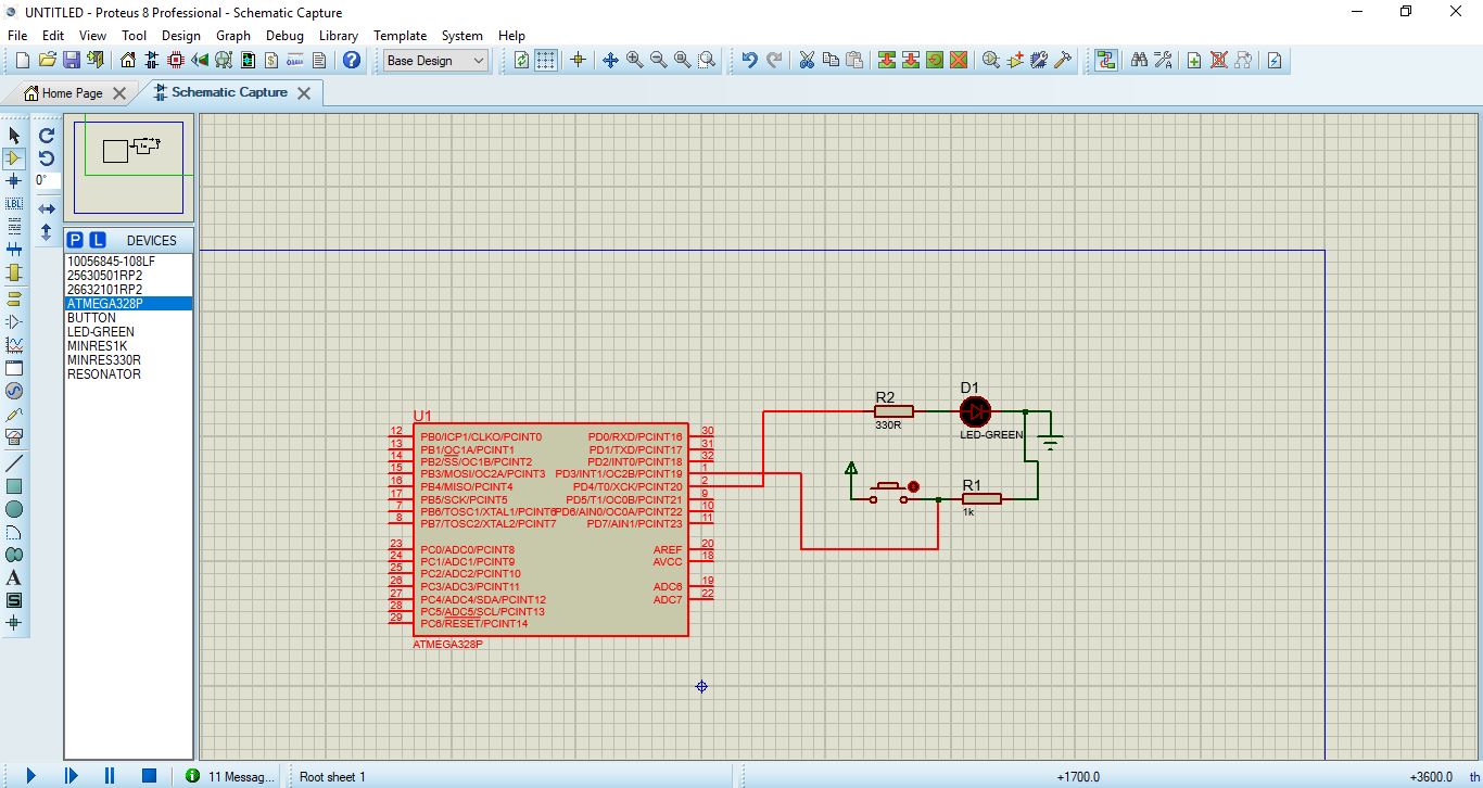
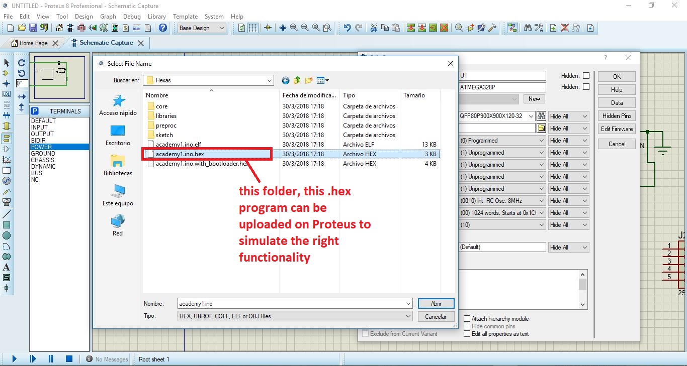
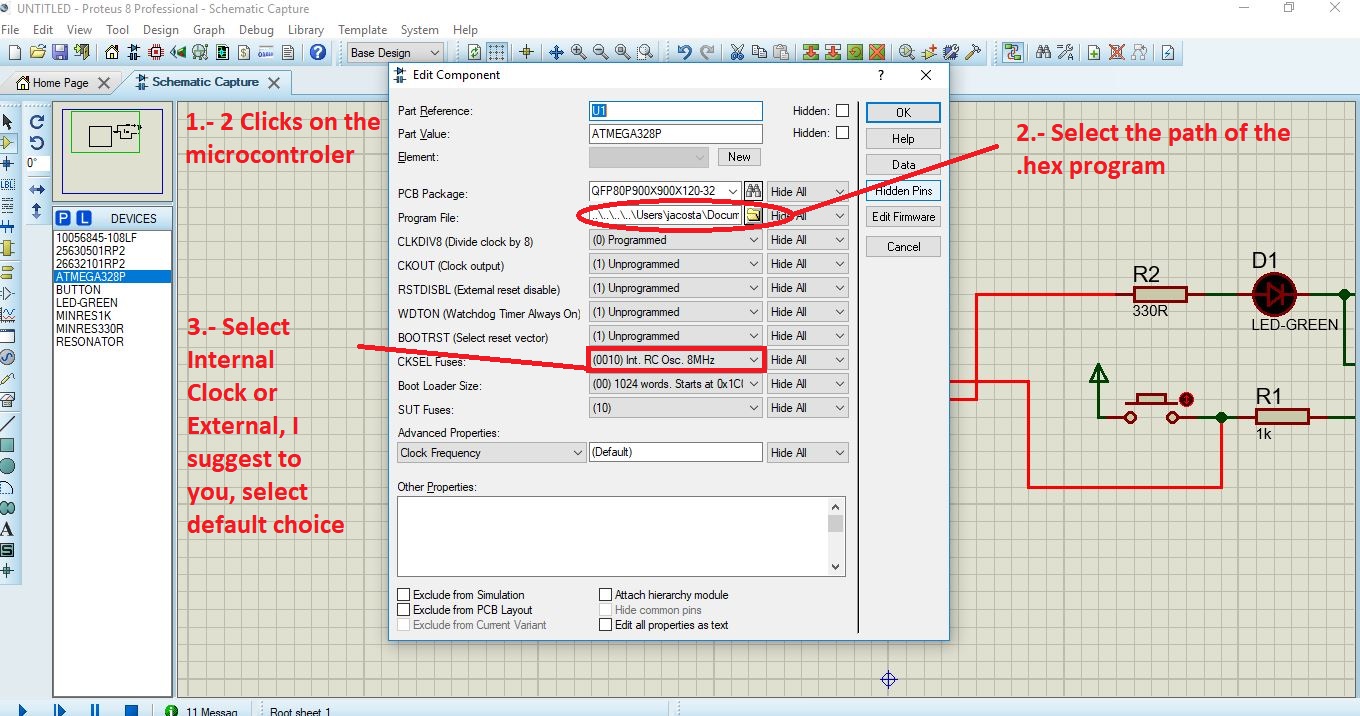
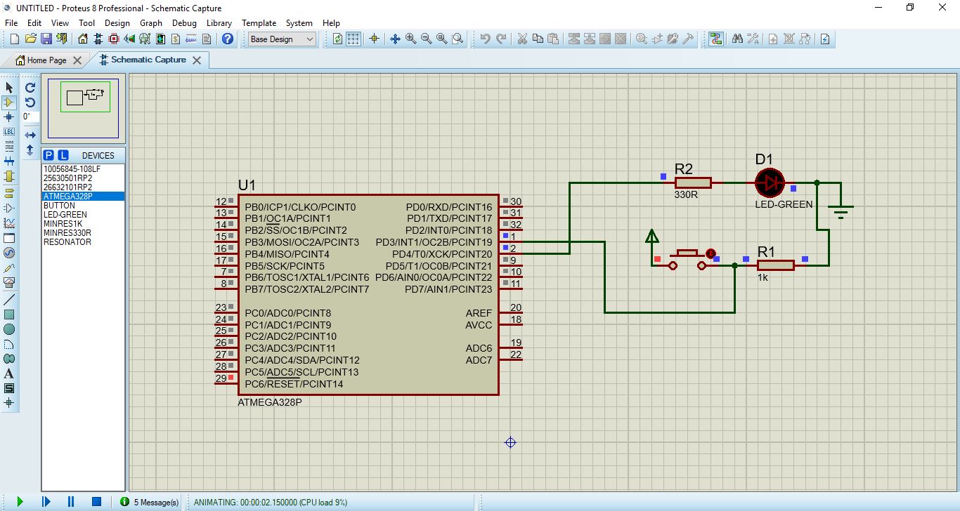
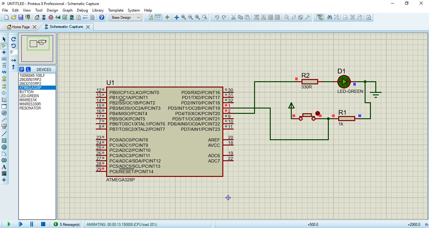
I started simulating on Proteus, for this is important to Install the software, when it is installed is necessary to create a new design.
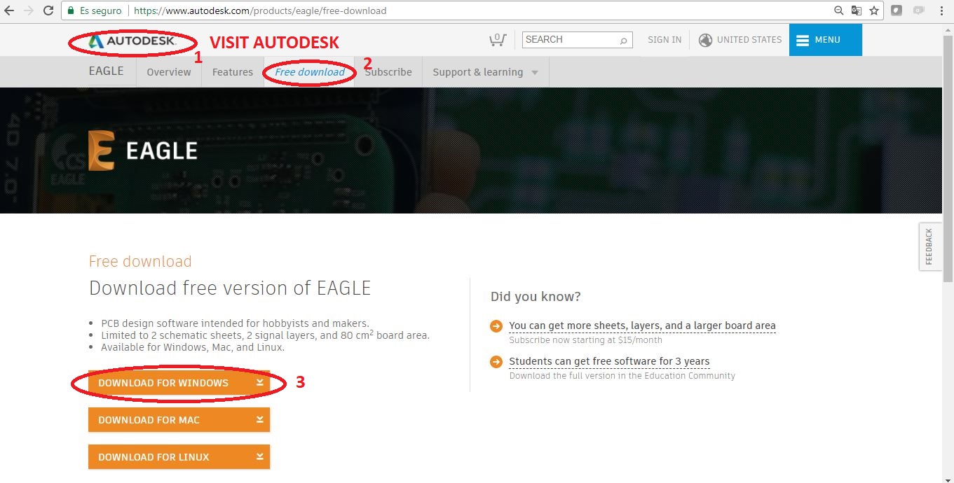
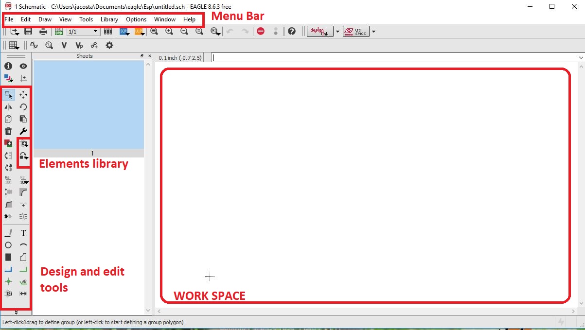
I will open Eagle, for this is important to download and install the software.
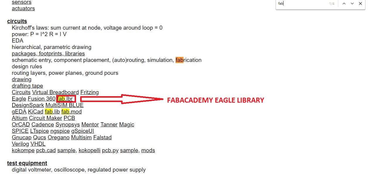
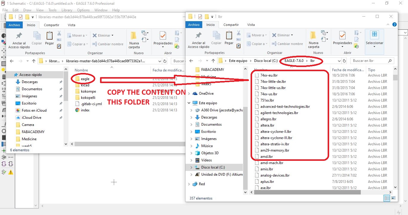
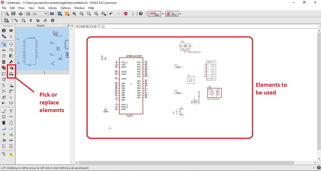
Once installed, is important to install elements libraries, for this I will use FabAcademy Eagles's lib. You can find more libraries on internet and move to the libraries folder
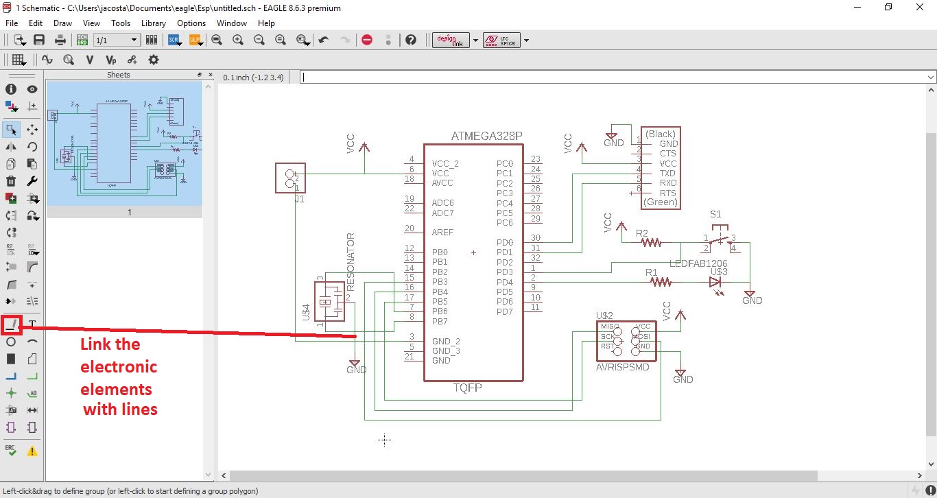
Then, let's open the software and create an schematic
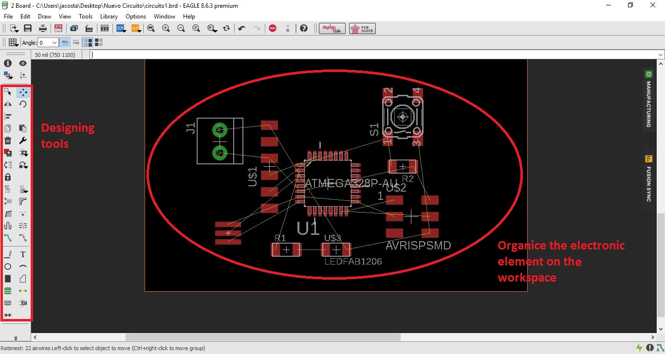
When I finished the schematic, I started creaing the PCB
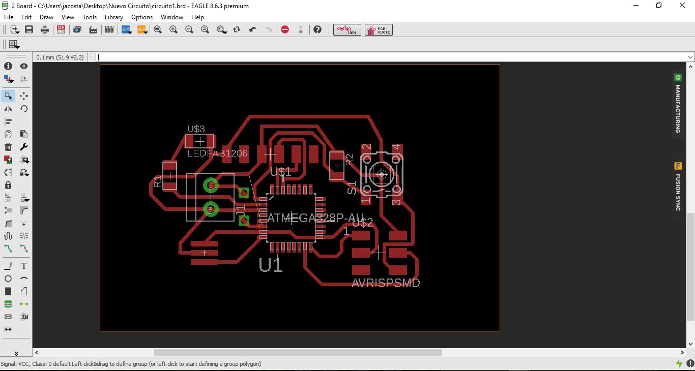
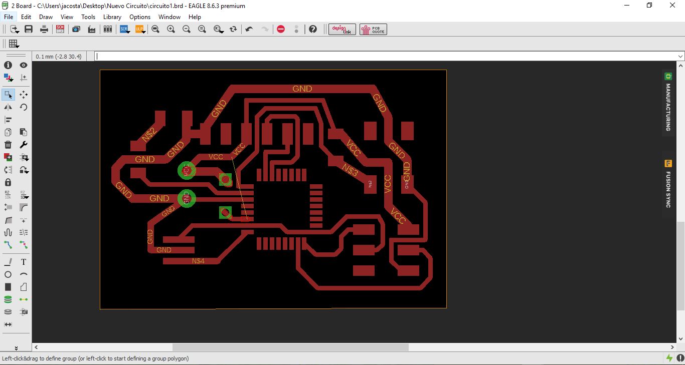
I will correct some problems on the lines circuit design
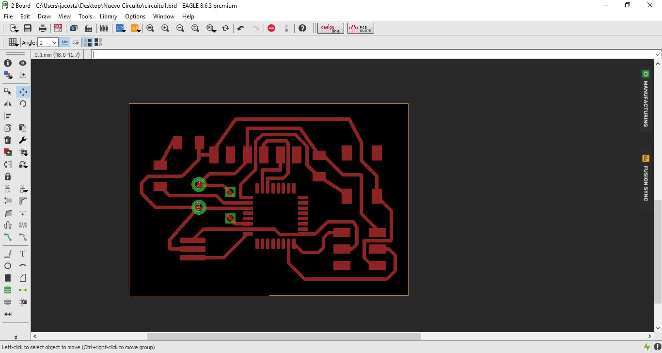
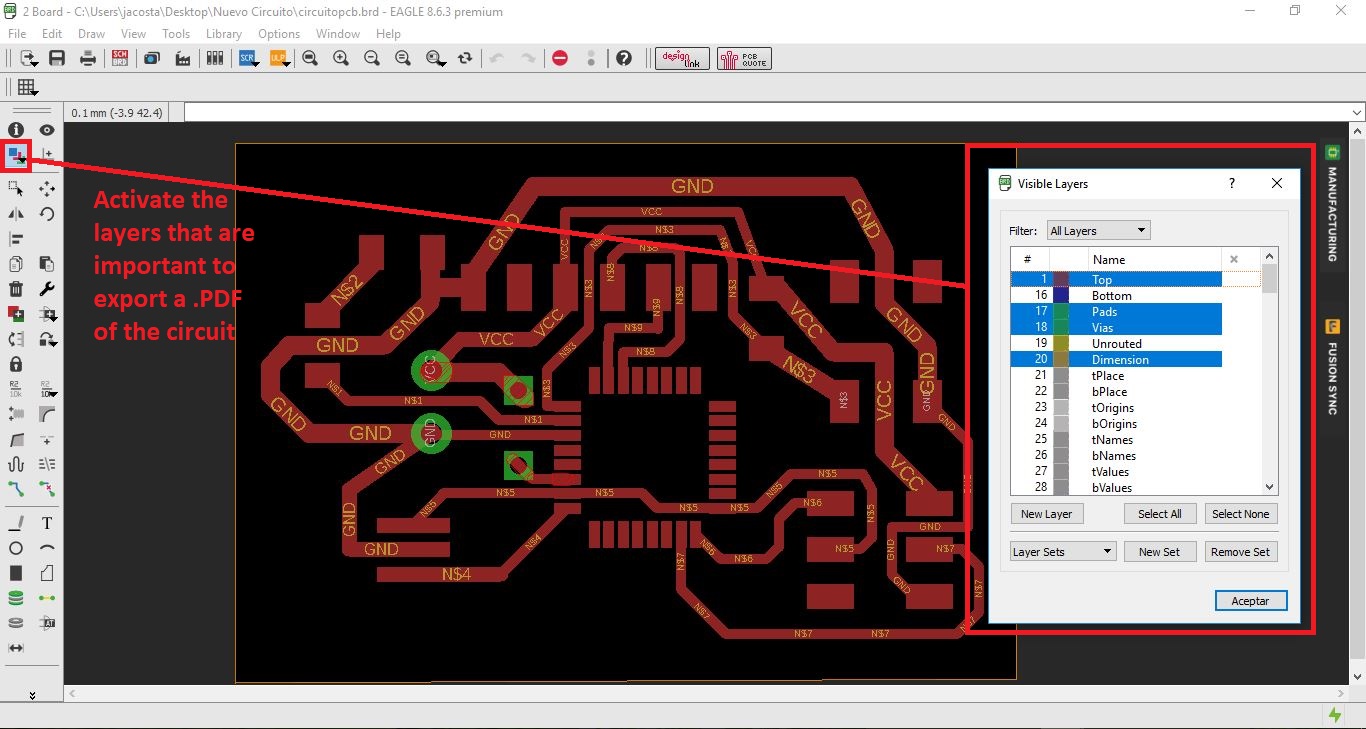
Now, I'll configure the layers to export the design to fabricate.
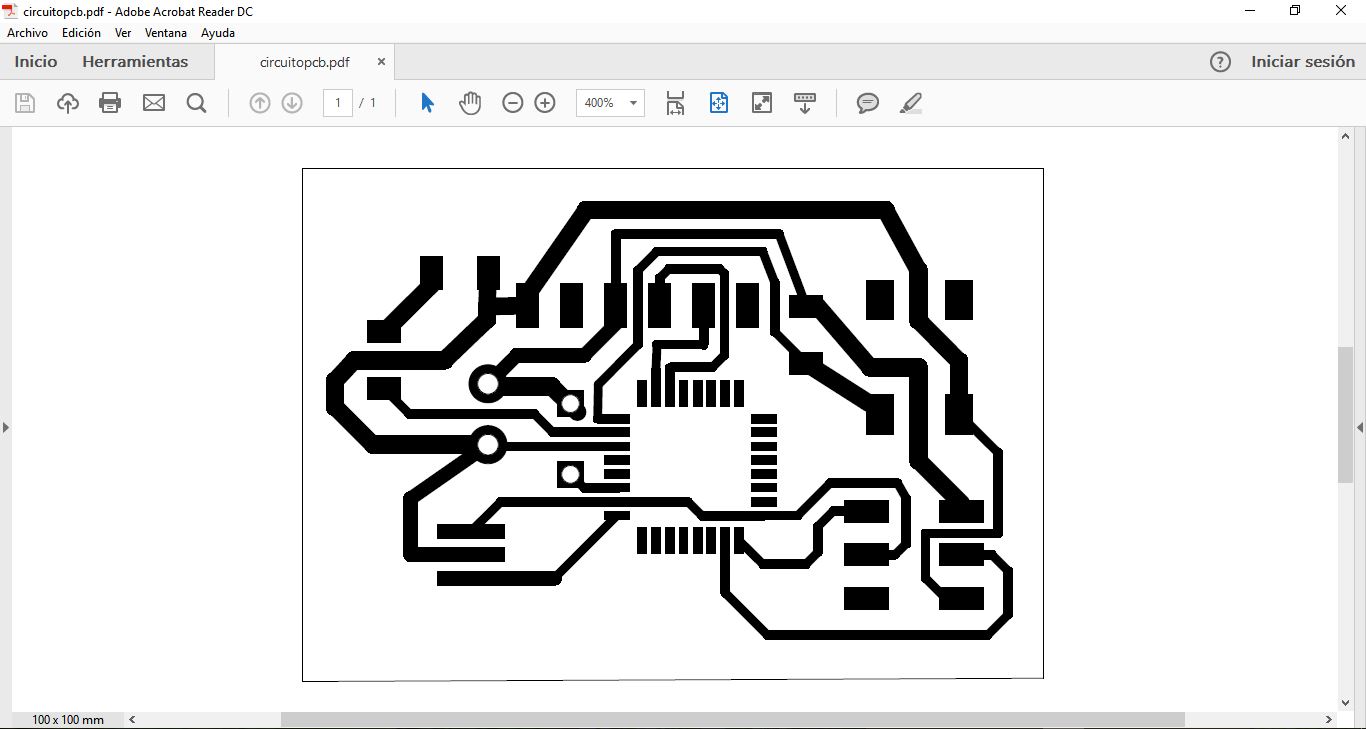
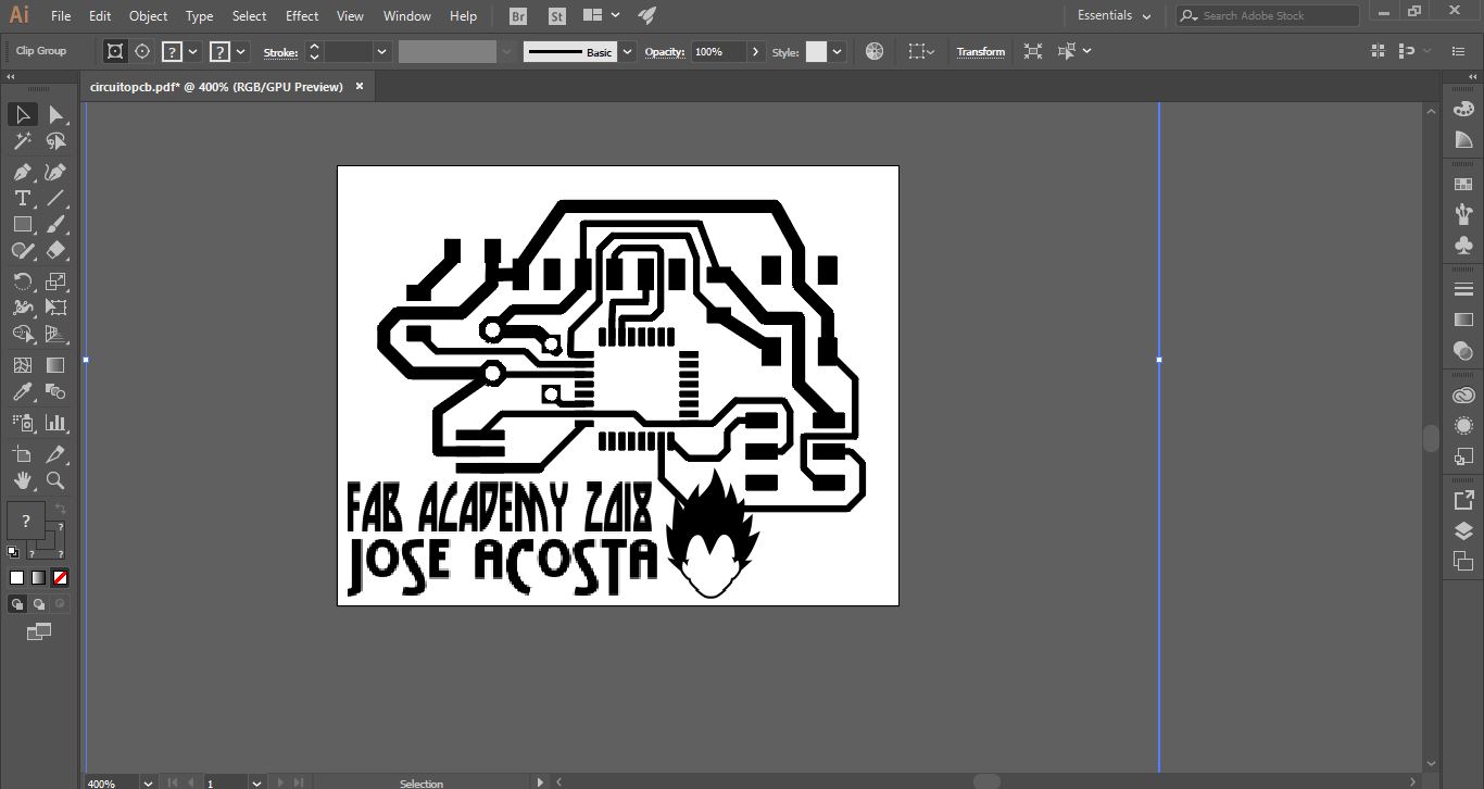
I have opened Ilustrator, then importr the PDF to personalize the design
The following steps are shown on week 5 and correspond to the process of preparing the files to mecanize the board with the design
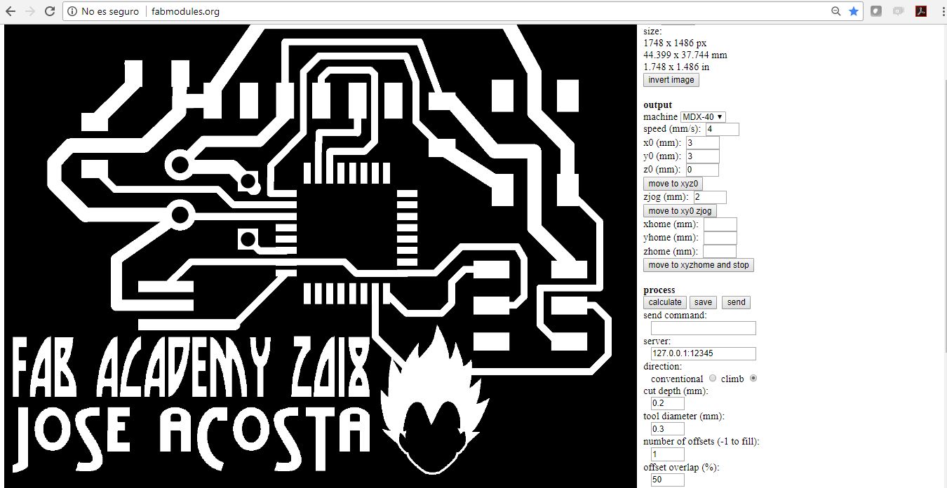
I will fabricate the board as a final step, for this i will import the PCB diagram to use FabModules.org, the procedure was shown two weeks ago, click here to go there.
Now is important to welt the elements on the board:
And the result is the following:
(SECOND EXAMPLE)
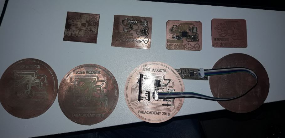
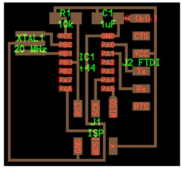
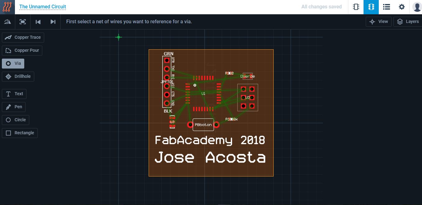
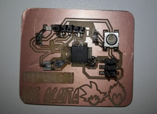
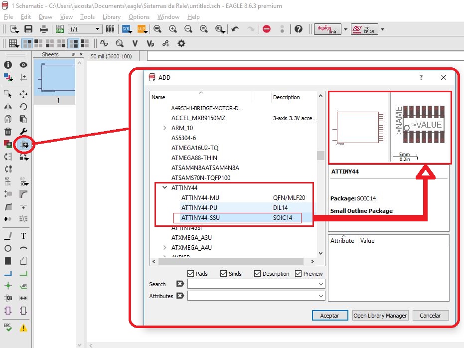
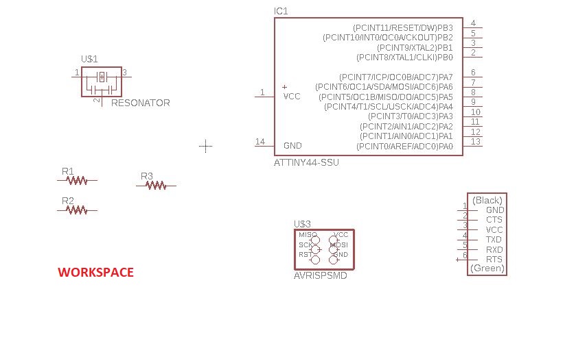
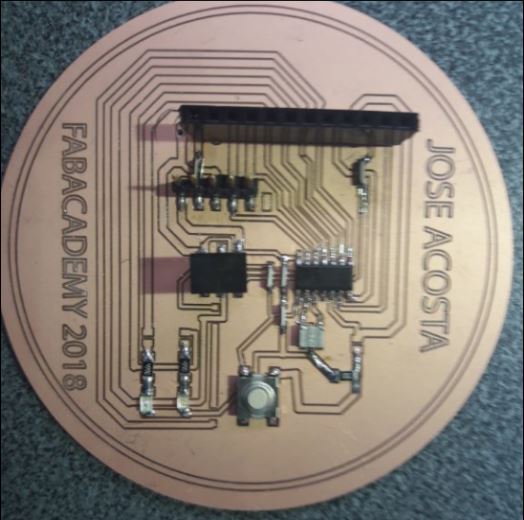
For this activity I will design an experimental board that integrates an ATMEL Atteny44 microcontroller and a series of jumpers so that I can perform the circuit bridging activity, completing the activity requirement of having at least one button and one LED. The reason for the plate is that it can work as a programmable plate depending on the activity that is required, it can be to test electronic circuits, to experiment with programming and to advance with the final project.
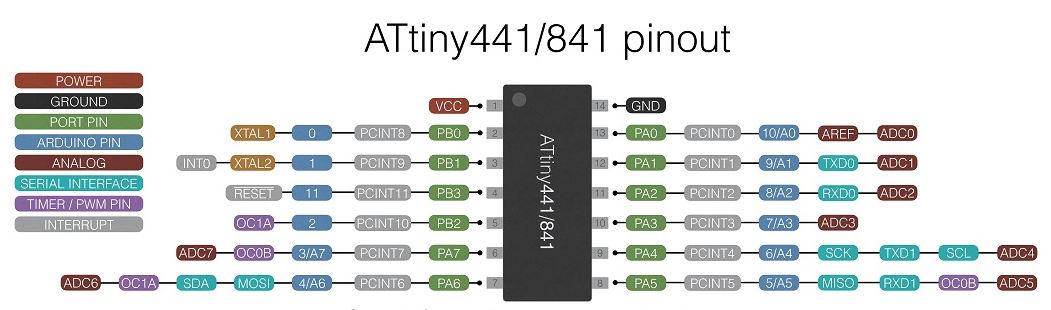
From the electronic design programs reviewed above, I will use Eagle for the development of the electronic circuit and for the design of the PCB and subsequent manufacture of the plate using the Roland MX-40 milling machine and using milling cutters of 0.1 mm
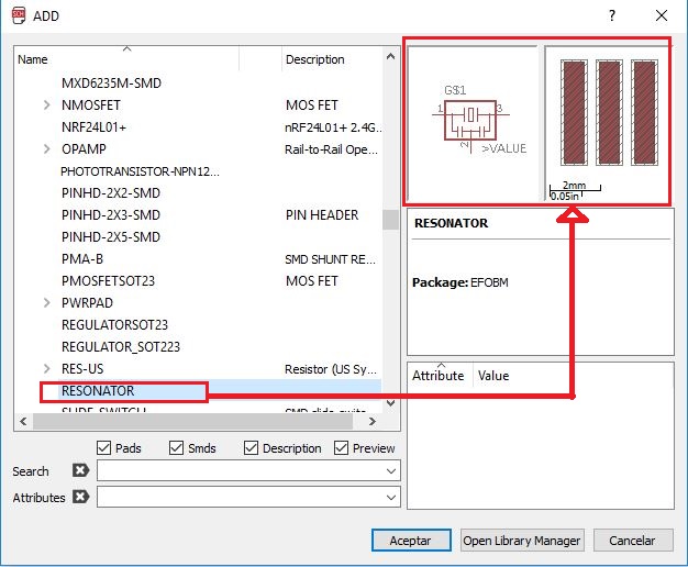
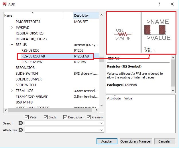
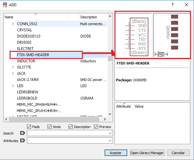
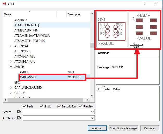
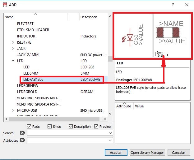
The devices that will be used in this activity are:
So, you should look for them in the device window and place them in the work area
Once all the necessary elements have been chosen, we link each electronic device by means of wires, it is important to analyze each connection pin so that they can be linked directly so that when creating the PCB there are no complications.
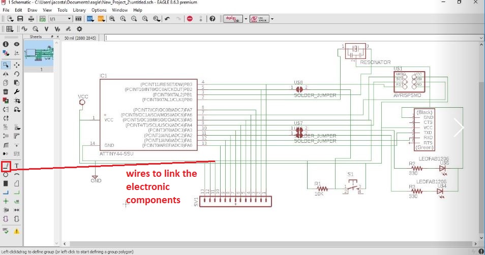
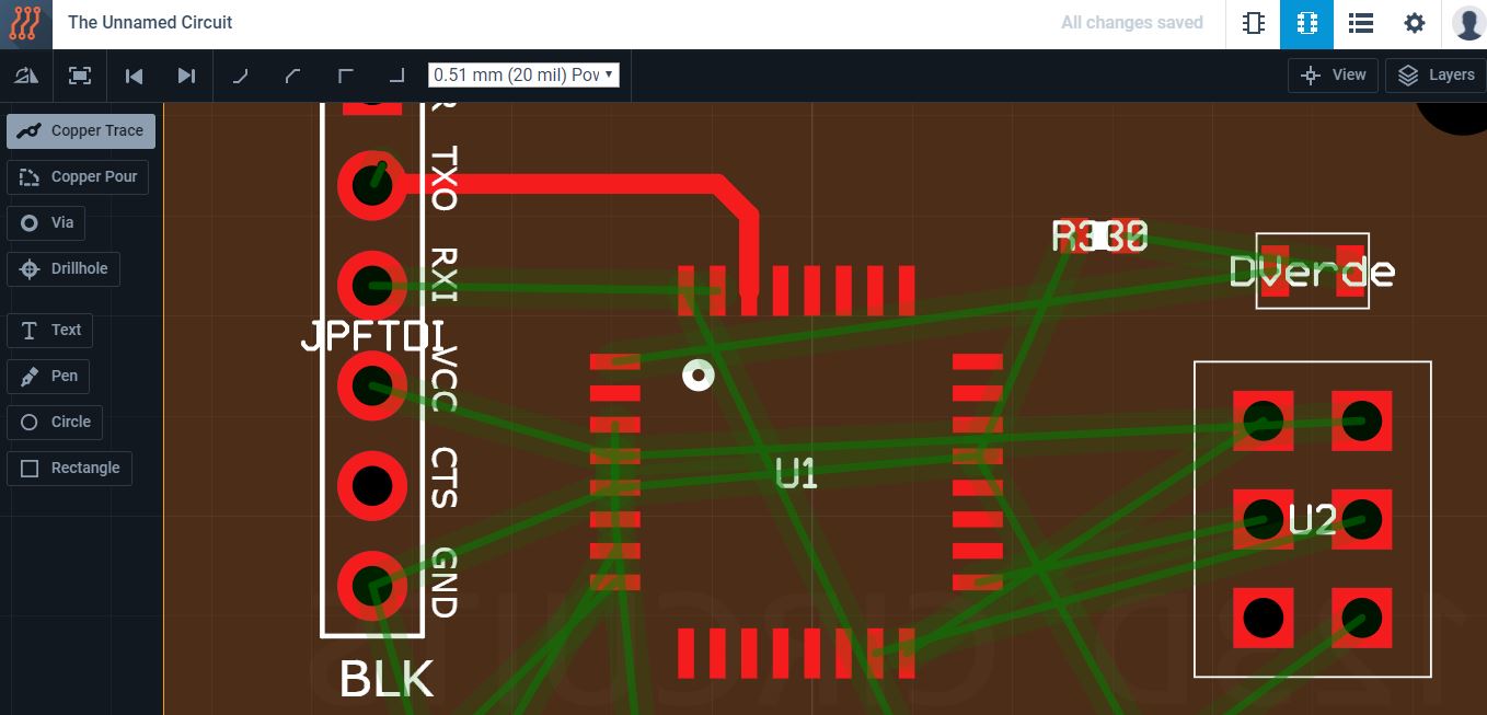
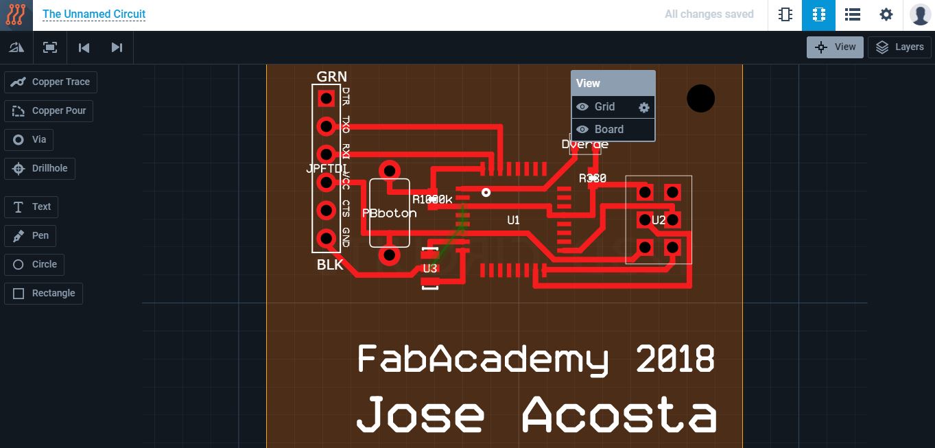
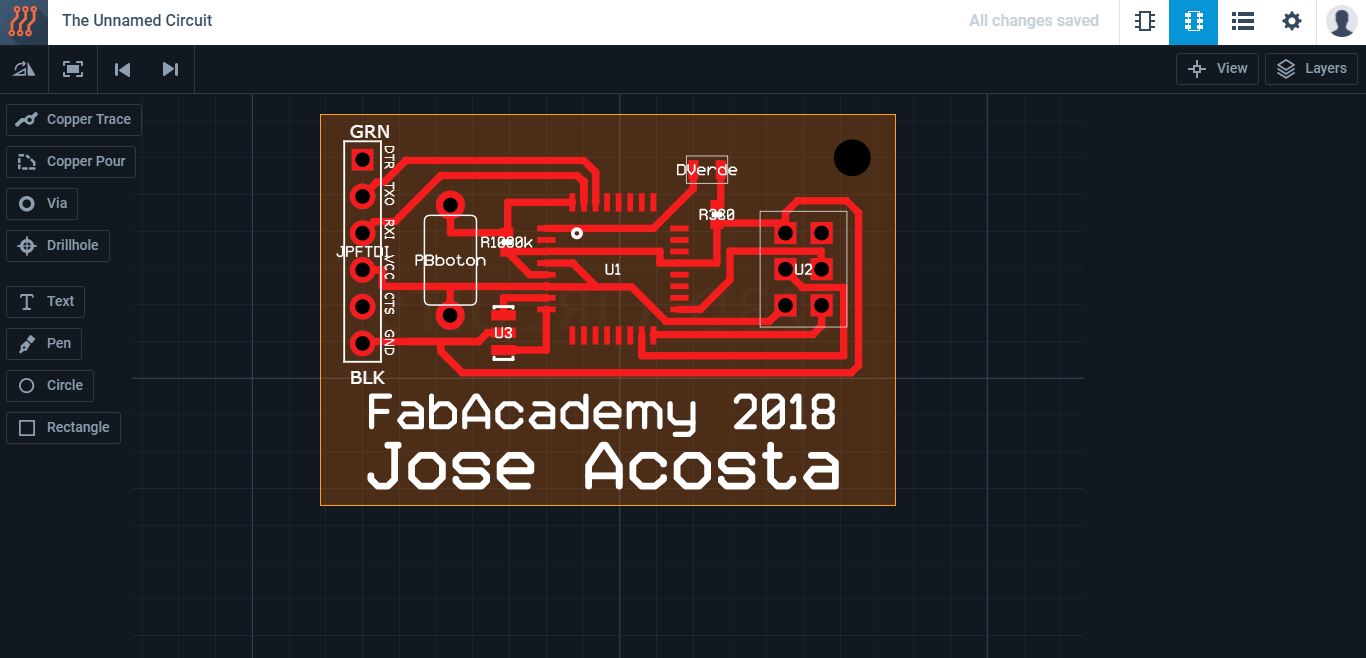
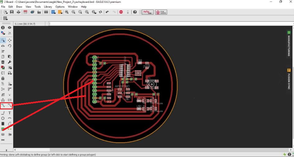
When the design of the electronic sketch has been completed, we start with the development of the PCB, where we display the PCB development window, the devices we select in the sketch design window will appear immediately, we will place each element within the element area, this area can be modified, for reasons of the activity I have designed it in a circular way. When electronic tracks are placed, we always have to check which is the best distribution of the tracks to create them and avoid unnecessary space costs.
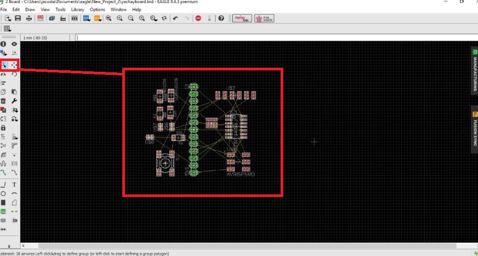
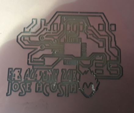
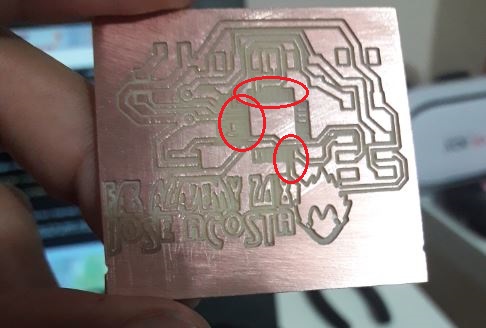
The plates must have thin tracks with a thickness limit to avoid that at the time of machining, can be lost and also between the spacing between posts should maintain a distance that does not affect the design between pestas, as can be seen in the figure below
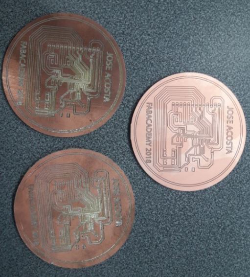
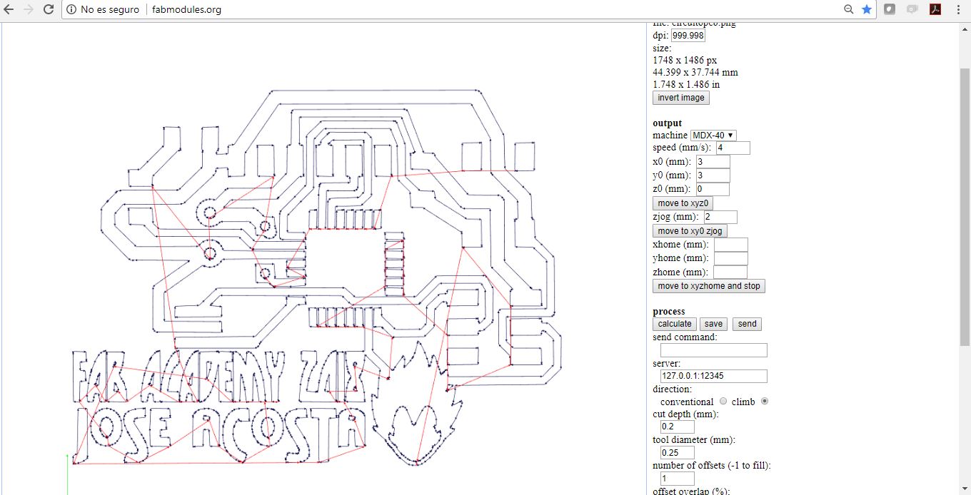
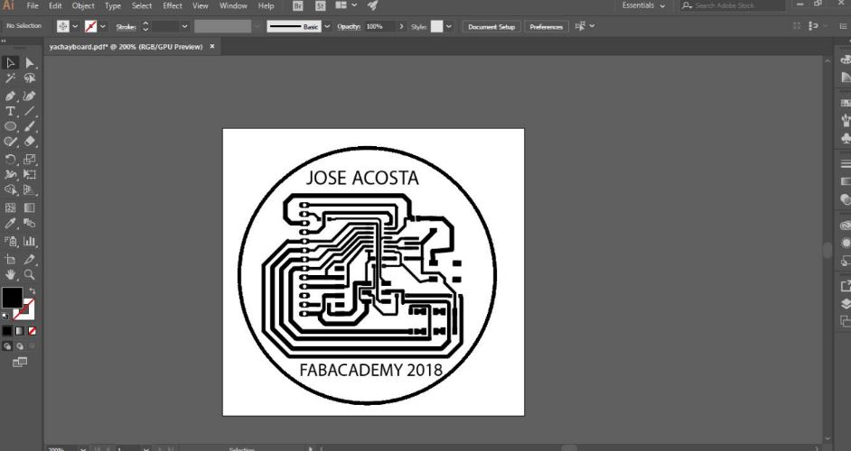
To make extra designs inside the board, it is recommended to export the file generated in Eagle with a .pdf extension and open it with the Adobe Illustrator design software, in this case I used the software to carry out the labeling of two phrases "FABACADEMY 2018" and JOSE ACOSTA. "

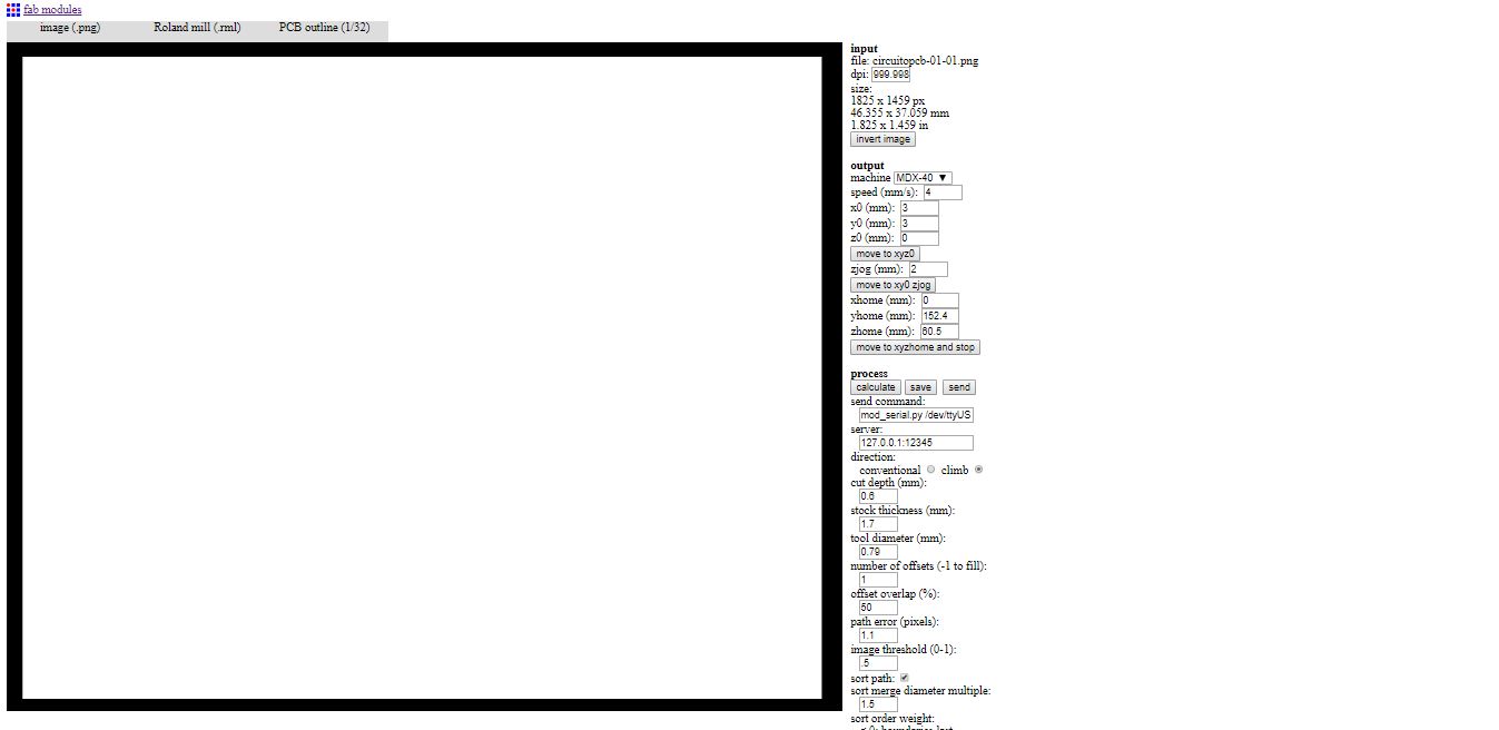
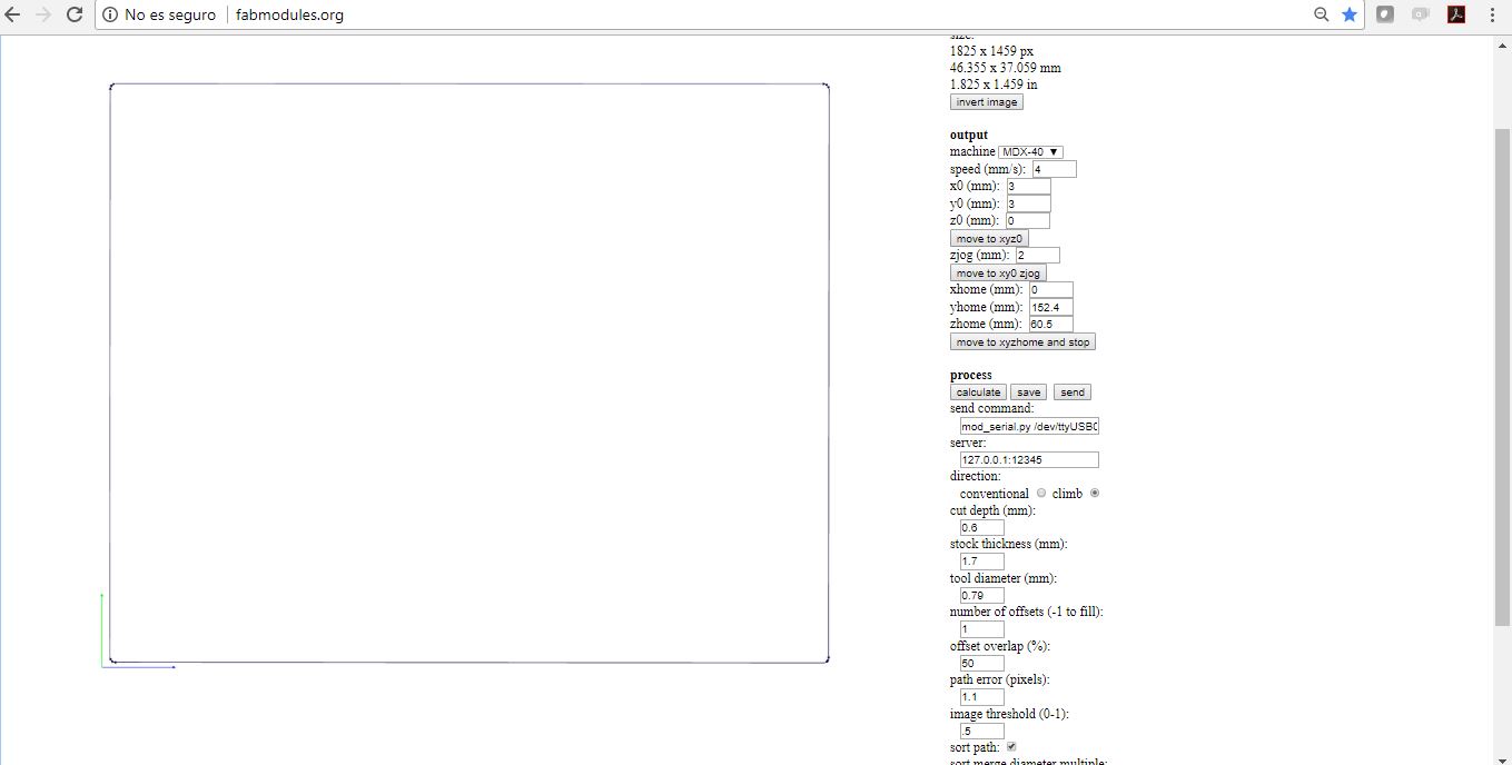
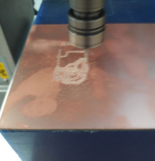
Then. I used FabModules (click here to go) to transform the design into G code. to mechanize, finally start mechanizing the board

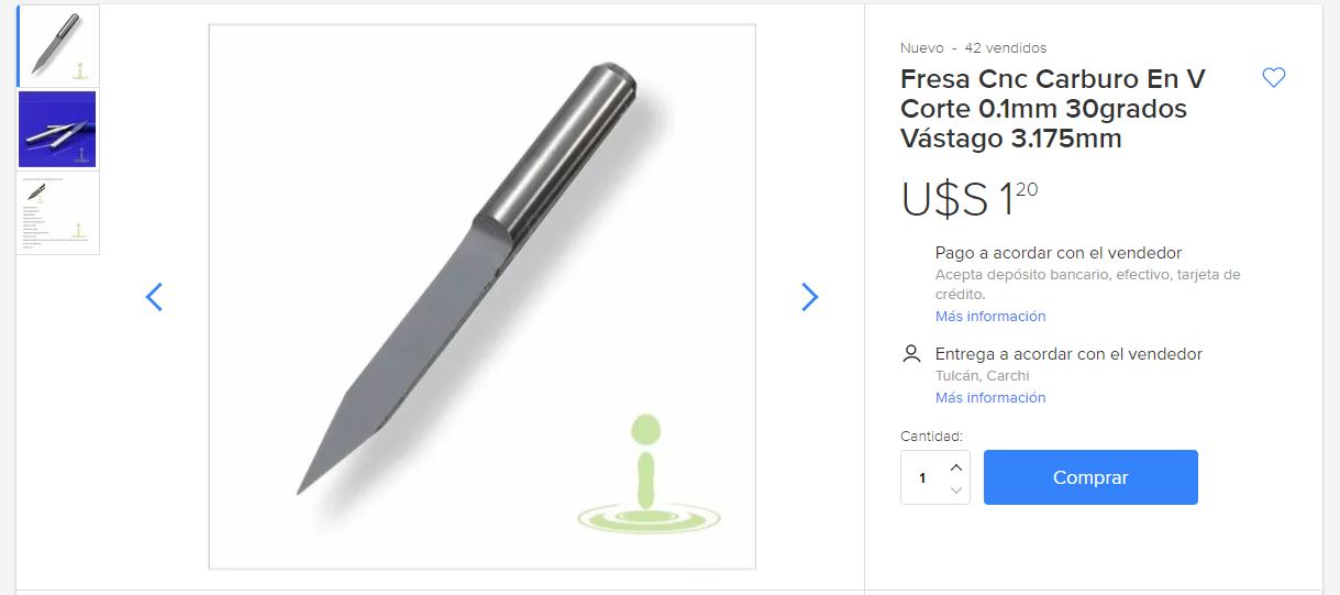
You have to be very careful in the design of the tracks, if they are very thin, when machining could be damaged and affect the operation of the electronic plate. to correct this activity I have purchased the following tip that could help to correctly machine the tracings of the tracks, and the design of 0.6 mm minimum thickness in the electronic design of the tracings of the PCB.
To solve the problem I have bought clic here to see the tip
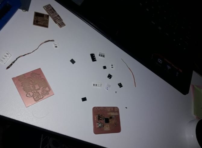
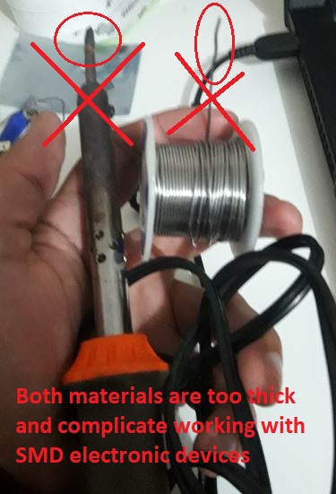
Another problem that existed in this activity is that for the first example a soldering iron with a very thick tip and very thick solder solder was used, which complicated the welding of electronic devices on the plate
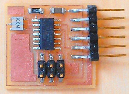
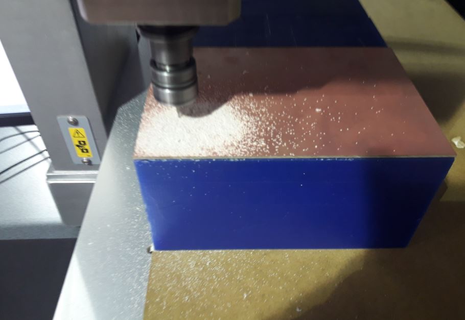
I have repeated some times the fabrication of each board to corret board, two boards has being grabbed with a wrong parameters and the third one has the best machining configuration, finally they work fine