Aim:
Understanding the machine and processes of PCB manufacturing
Task 1:
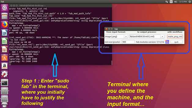
Getting to know the machine
The process that we generally use is the process of milling for production of PCBs ,
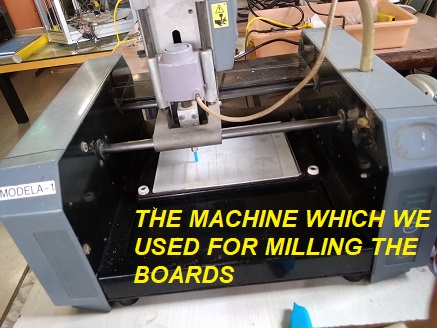
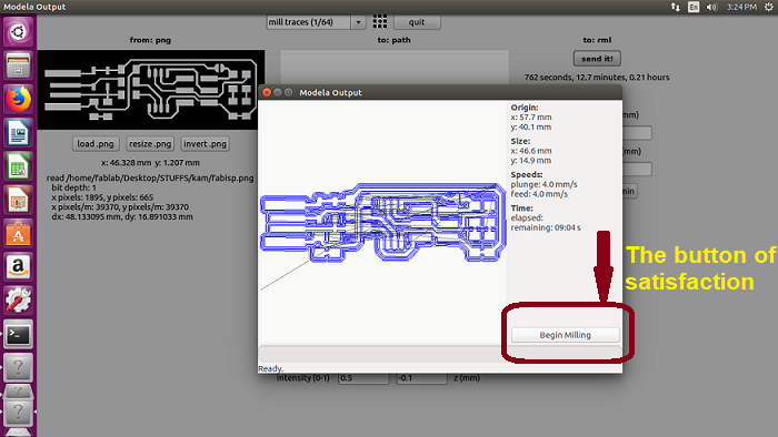
The machine that we have is modella MDX20 , a basic milling router that can be programmed through mods or fab module(in our case)
It has a bed size of 150 x 200mm
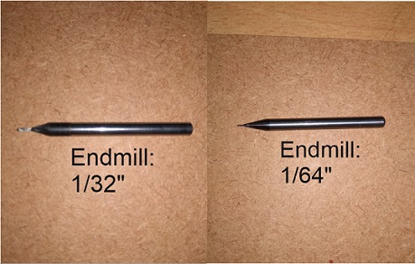
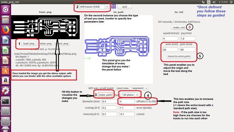
The tools we used were end mills of sizes
1/64 inch for milling the tracks
1/32 inch for cutting the board
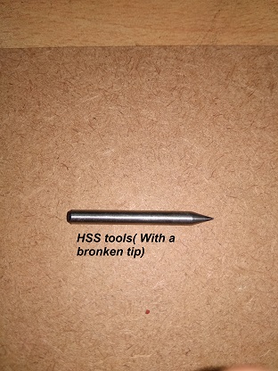
There were two materials that we used for tooling
- Hss (high speed steel), which broke due to improper fricturing and a reason more that following image explains better.
- Carbide , these tools have a body made out of hss and have metal carbide inserts at the machining edges, this provides an extra strength for machining operations and the tools has longer life. (Shown in the images above)
Group Assignment
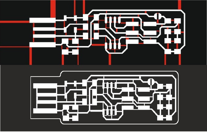
In this assignment we decided to mill a pattern which displays the thickness and the tolerances of the drill bit, so for this one we decided to use the standard 1/64" endmill, and achieved the following pattern..
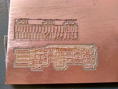
Out of which we concluded that:
- Some of the tracks were not printed because the bit we used was a standard bit of 1/64", and the tracks width of the image was so small that the bit was unable to calculate it's milling offset in the region and hence it didn't mill, but rather if the bit was of 0.010" it could have possibly reached there.
- The threads that appear in the image are a result of vibrations produced in the machine which reached till the drill bit and makes it shake to produce the threads
- The tracks in the PCB milled below have wobled because the bit we changed was a new one and has some manufacturing deffects hence it blows of the tracks
- Hence for the fiqure to be perfectly milled we need
- A perfect fixturing method(A standard tape for fixing the PCB that could avoid the vibration)
- A drill bit as fine as having diameter of 0.001mm
- A drill bit that has no mechanical deffects as a runout, or tapered end.
Task 2:
Milling the PCB
For this we actually didn't had to design the board instead just pickup the board listed in the Assignment page
For the same I found Brian's Board, a bit easier in terms of components and it was also well refered, hence without going much into design I downloaded the PNG for the tracks and milled it...
Following was the process we followed for milling the board is well explained in the pictures below,
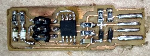
Out of which I got my final board as seen here..
Task 3:
Task 3:
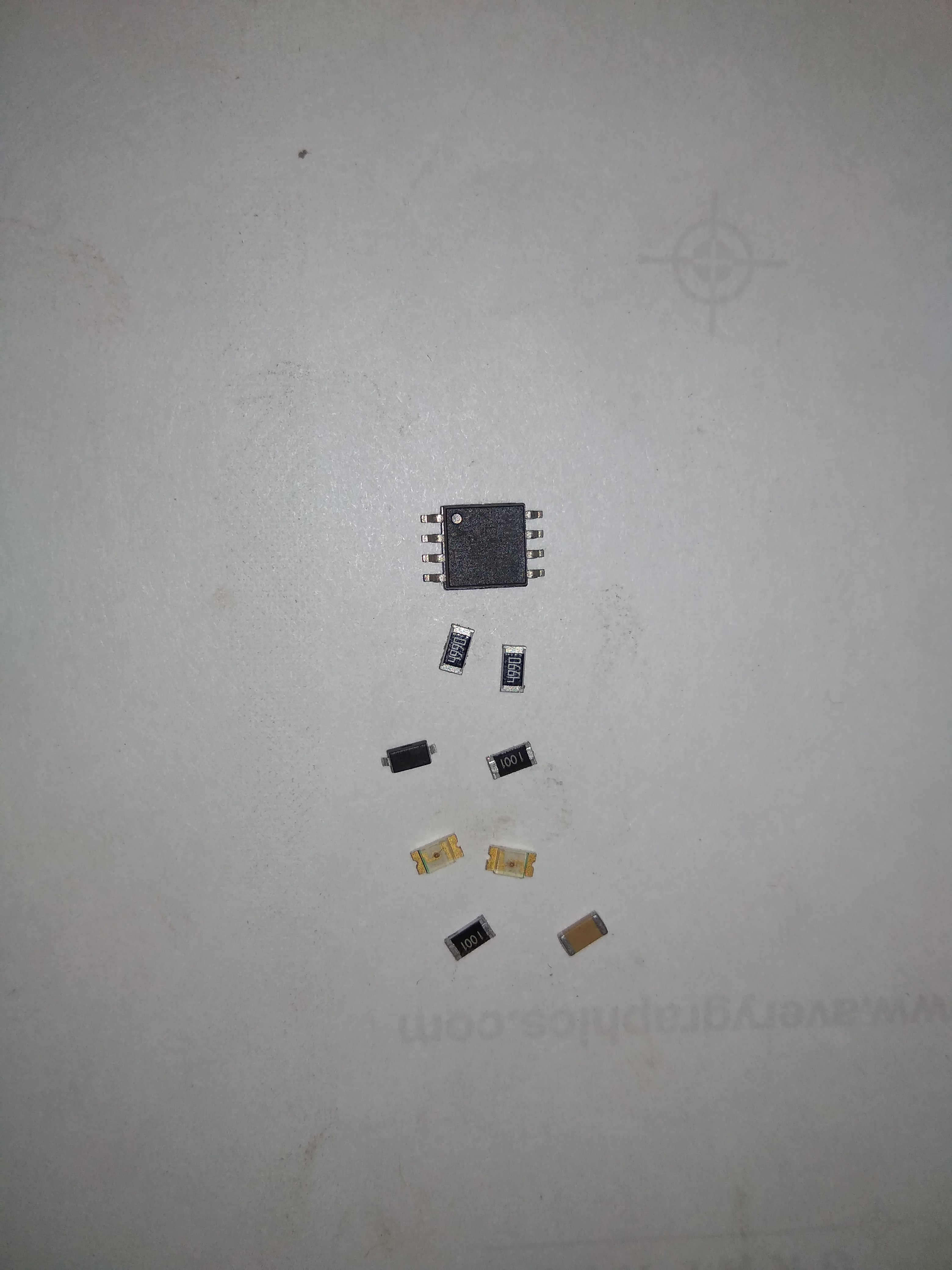
Hunting the components
After this there comes the process of hunting the components, you have to select the components precisely in order to support the function of ur IC
For this assignment we needed.....
Task 4:
Soldering the components
So basically what is soldering??
It is a process of fusing and applying metal over another to create joints Here the metals we had were, Copper PCB and soldering wire made out of alloy of lead
The Process
It was naturally a tedious task since j had never done it before and more over the maximum size of the components was 1.5 mm, that became a lot difficult to handle But out of few tries and errors I came to a method that worked for me and is rather suggested as the standard one
- Make a spot of solder of on the blank PCB
- Hold the component on the spot and heat the spot to fix the component
- Solder the second end of the component directly
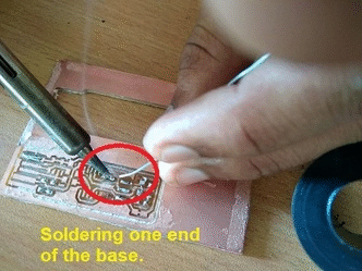
This method proves to be better because one joint provides the anchor initially when u solder the other joint
Sub Task:-To identify the polarities of the components, while soldering
There are two methods 1 is by using multi-meter , thats the most reliable method since you directly connect the components to a circuit and if they work u get the polarities.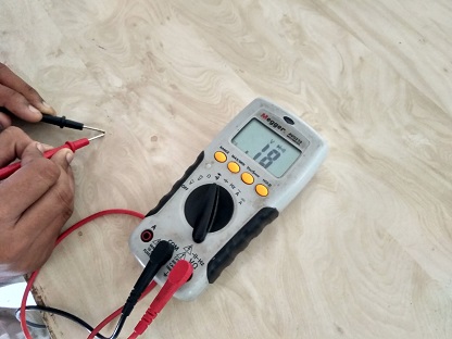
Other is by looking carefully on the components
There are many identification marks on the components:-
- The green mark on the LEDs indicate negative side
- A line on the zener diode indicates negative
- A dot on the IC indicates ground terminal
Rest resistor and capacitors can be assembled anyways.
Hence considering all the parameters above one can look through initial stages of manufacturing of PCBs.
Problems faced and Solutions applied
For this assignment i actually faced few problems regarding the machine, and few with the skills required for soldering, since I was quite a noob for it.
Some of them are listed below...
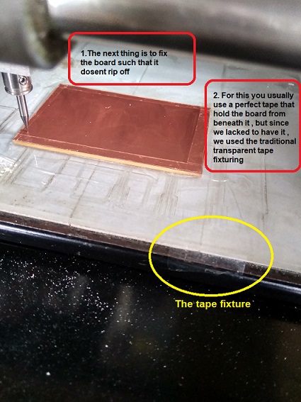
1. The basic problem with milling the PCBs was the issue about fixing the board to the bed, when the tool of 1/32 inch was used the board used to come off with the blade since the adhesive on the tape was pretty weak.
Solution:-
For this we made a temoraray fixture out of transparent tape which would hold the board in place and avoid the loss of time untill the better tape arrives.
2. Following described was the only problem regarding the machine, later what i face was with the soldering part of it, because it was actually my first time to hold a soldering iron in my hand and assemble components that small, it was all together a tedious task.
During this i was unble to guess a fact that when i over heat the tracks thtey could come out, and similar happend when i heated the components to remove them , the tracks got over heated and they were pealed out
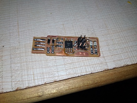
Solution:-
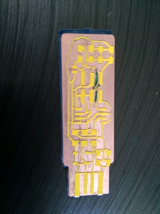
For this the solution was to change the board simply and then solder that board with ample of care. Which I followed and finally got a board which now appears like following.....
Task 5:
Programming the pcb
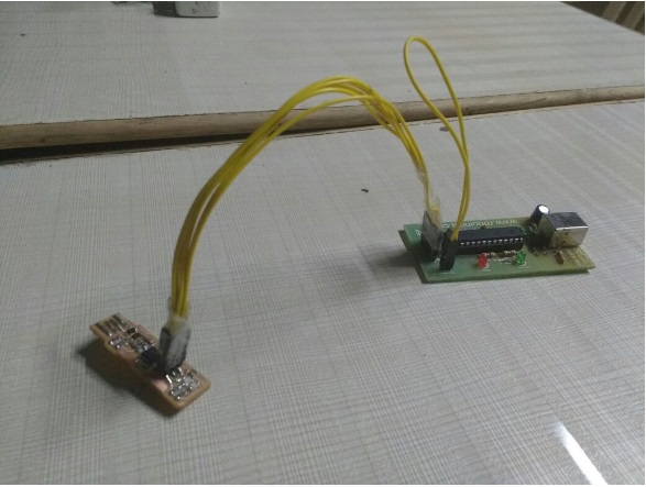
Initially we did our programming with a commercial board.. Which looked as follows:-
This task had been bit difficult since I was quite reluctant to install ubuntu, hence what I had to do was to install git bash, for this you just download git bash from this link..
Click Here
Then after installing and cofiguring git bash(follow the instructions of the setup), again because of being in windows I had to install few more driver softwares that included.(Download links mentioned)
For the above two(...) you dont have to install them as such in, what you do is only extract the files into "C:/Program Files"
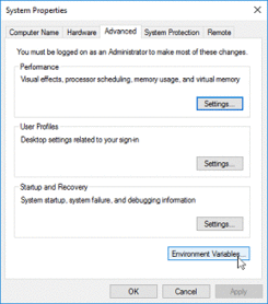
Then the next step is to add the files into the device registry for which the following image guide you well..
The next step ypu have to install and connect to the "Zadig" and then you follow the steps below:
- Attach your soldered board to the programmer through the 2 X 3 pin header,and attach the programmer to the usb of your machine.
- Then search usb isp in the drop box, if it shows nothing, just click on options and "List all devices"
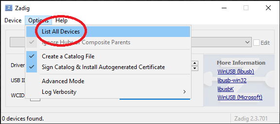
- Then hit install drivers and you are good to go
Following commands end your task with the Zadig
The next thing you can do is open git bash and then type following commands, and identify the results
- make -v and press enter.
You should see: GNU Make 3.81 Copyright (C) 2006 Free Software Foundation, Inc. - avr-gcc --version and press enter
You should see: avr-gcc.exe (AVR_8_bit_GNU_Toolchain_3.5.4_1709) 4.9.2
- avrdude -c usbtiny -p t45 and press enter.
You should see: avrdude.exe: initialization failed, rc=-1
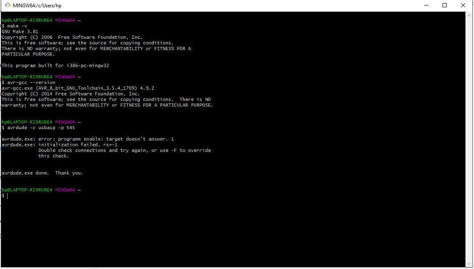
If all of the results are seen as given then your PCB works just fine if not you have to debug the problem,
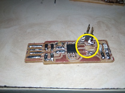
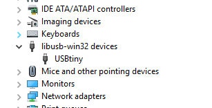
Problem I faced
In my case the bash was giving no results it would give a blank out put, which when i debugged I found to have a current leak in my soldering which had to be fixed, and later I was able to achieve it.
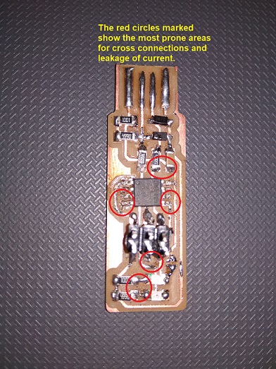
Major possible points for current leak can be viewed in the image below
Preferably the installation of the drivers end here, the next thing that comes by is installing the firmware and then cofiguring it with your fab-isp, so that now it would behave as a new programmer.
This is done through following steps.....
- Initially download the firmware from this address.
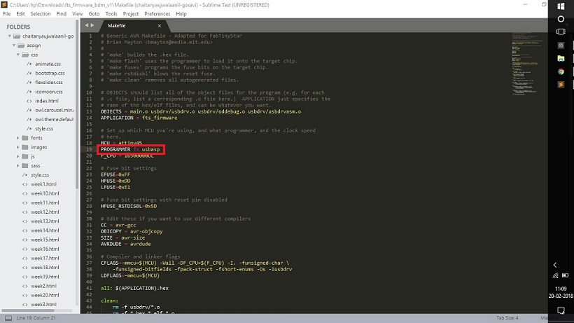
- Go to the folder and open the file named as "make" in any text editor, and then in the programmer tag, replace anything written with "usbasp"
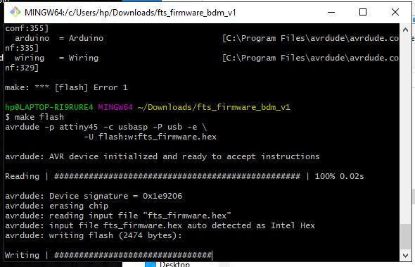
- Then open git bash again, navigate yourself to the folder and then run the command "make flash", this gets the firmware written on your fab isp
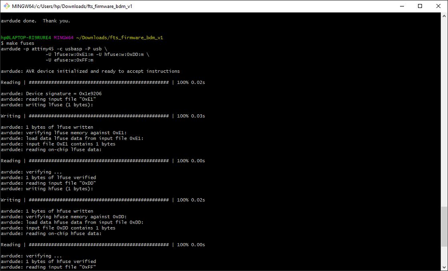
Then run the command "make fuses" if you see the output as below, it means the isp runs successfully and now you are done with your stuff
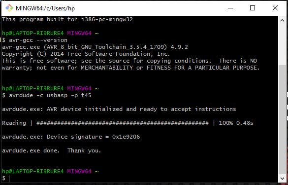
- Then run the command "avrdude -c usbasp -p t45"
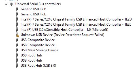
Later when I installed the Adafruit driver the board was finally detected.
Task 6:
Exploaring other methods to produce PCBs
For this task I wanted to try the process of etching and build a board using that process.
What is etching??
Etching is a process of removing a particular layer of the material by making the layer react to a particular soltution (considerably having more reactive ions for the base material to disintegrate), and leaving the desired layer covered under any non reactive surface, of vinyl or an ink.
Hence you get the desired surface that dosen't disslove beacuse of the coating provided.
Process Followed
Following were the steps along with the problems, which I followed to build up the circuit
- Initially i had just printed the the *.png file of the circuit directly which had became an intense workout for me since the vinyl cutter lacks the accuracy to cut perfectly, thus some of my tracks were not perfectly cut, which when I tried to pull of manually, didn't work because it was actually difficult to cut somethign that small and complicated
- Later I tried generating segments between two patterns that provided a well divided strata for making it easy to cut....
- Later I finally went for a step of cutting the entire piece and then transfering the pcb to a blank board which was in the shape of fab-isp and then remove the masking and then soldered it later.
Problems faced
There were actually plenty of problems
1. The vinyl cutter was not so accurate to print the circuits properly, it actually rippeled off the circuit prints as shown below..
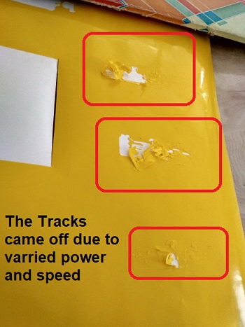
As a solution of which I changed the speed and the force setting to a higher speed other than normal and a comparatively higher force of 130, which got me a clean cut circuit.
2. Then the problem was with peeling the circuit, since initially the circuit was a whole block, it became difficult to peal it off, but later it was solved by making snippets as shown above.
3. Later I had to etch the board, so the solvent that I used was a proportionate combination of FeCl3, Distilled Water, H2O2...
The solution probably appeared orange because the FeCl3 was quite old and had oxideised
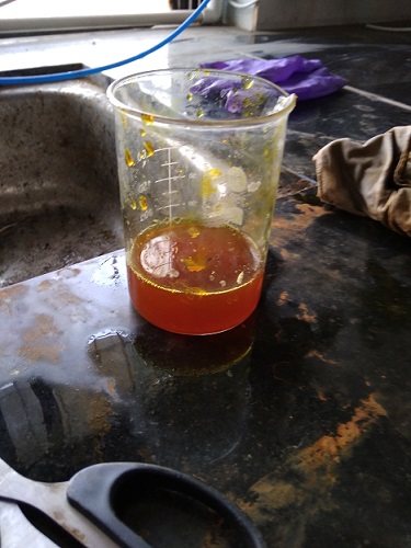
4. Then I poured the solution into the petridish and then placed the boards deep inside the solution, as shown below..

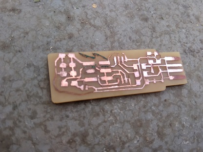
5. Finially after removing the vinyl layer, I got this as a perfectly etched board
Hence ends my journey through the week.....