Aim:
To understand input devices and their working.
Task 1:
Understanding the the basic priciple behind the Input devices
Basically the devices which generate data from the real world to communicate with the electronic interface to show us desired results are termed to be input devices.
These include a variety of sensors, switches, controllers etc
The input devices we had chosen to work with were various sensors, and the methods by which the data from the sensor could be analysed.
The methods known to us were..
- Plotting the wave using oscilloscope
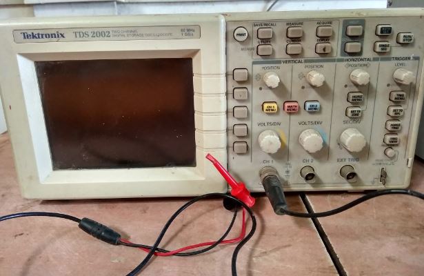
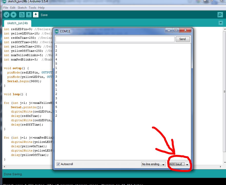
- Using the serial monitor of Arduino IDE to view the data in terms of digital signal
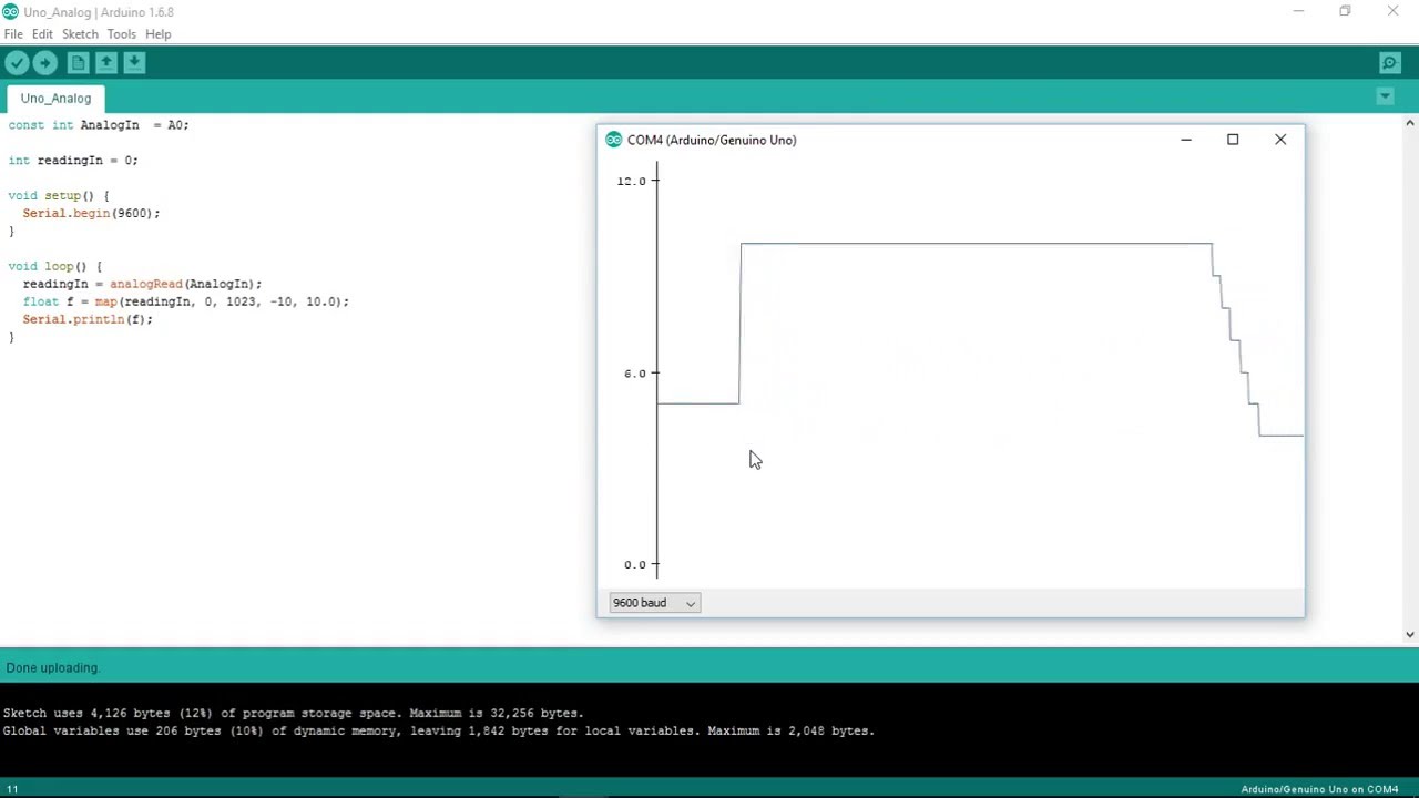
- To use serial plotter of Arduino IDE to view the data in wave form
Generalised Working
A particular sensor basically measures the relative difference between the parameters specified to it, for instance, the example shown below is of a Sonar sensor which generates high frequency sounds(above 20Khz), and then calculates the distance from which it reflects.
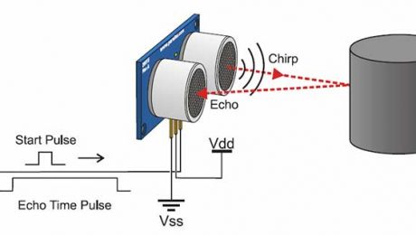
This basically generates a digital pulse which is directed towards a pin of a micro-controller which is programmed to read the input from the signal, in terms of binary digits or waves.
Task 2:
Group Assignment
The group assignment that we had for this week was to measure the digital and analog signals for a particular sensor.
For this we had used the serial plotter and monitor of arduino and then the Digital Oscilloscope that we had.
What we had aimed was to sketch a random circuit and see how the readings are actually poltted in the form of waves and number..
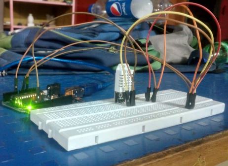
Hence following was our circuit for the assignment, where we had attached a DHT22 (thermal sensor), to an Arduino and had burned the program over it to check the needful results..
Task 3:
Designing and Machining our boards
There was actually a very good way that we had opted in our group assignment for testing the sensors, that was using the arduino.
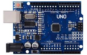
But for this assignment we had to develop our own boards to analyse the sensor.
The sensor I had desired to work with was the ultrasonic sensor
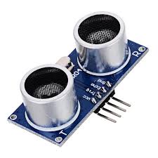
Because this was going to be a build up step towards my final project, i wanted to learn the feedback system of this sensor to use it in the final project.
Hence i decided to use a board that could be directly used for further assignments to come along with the final project.
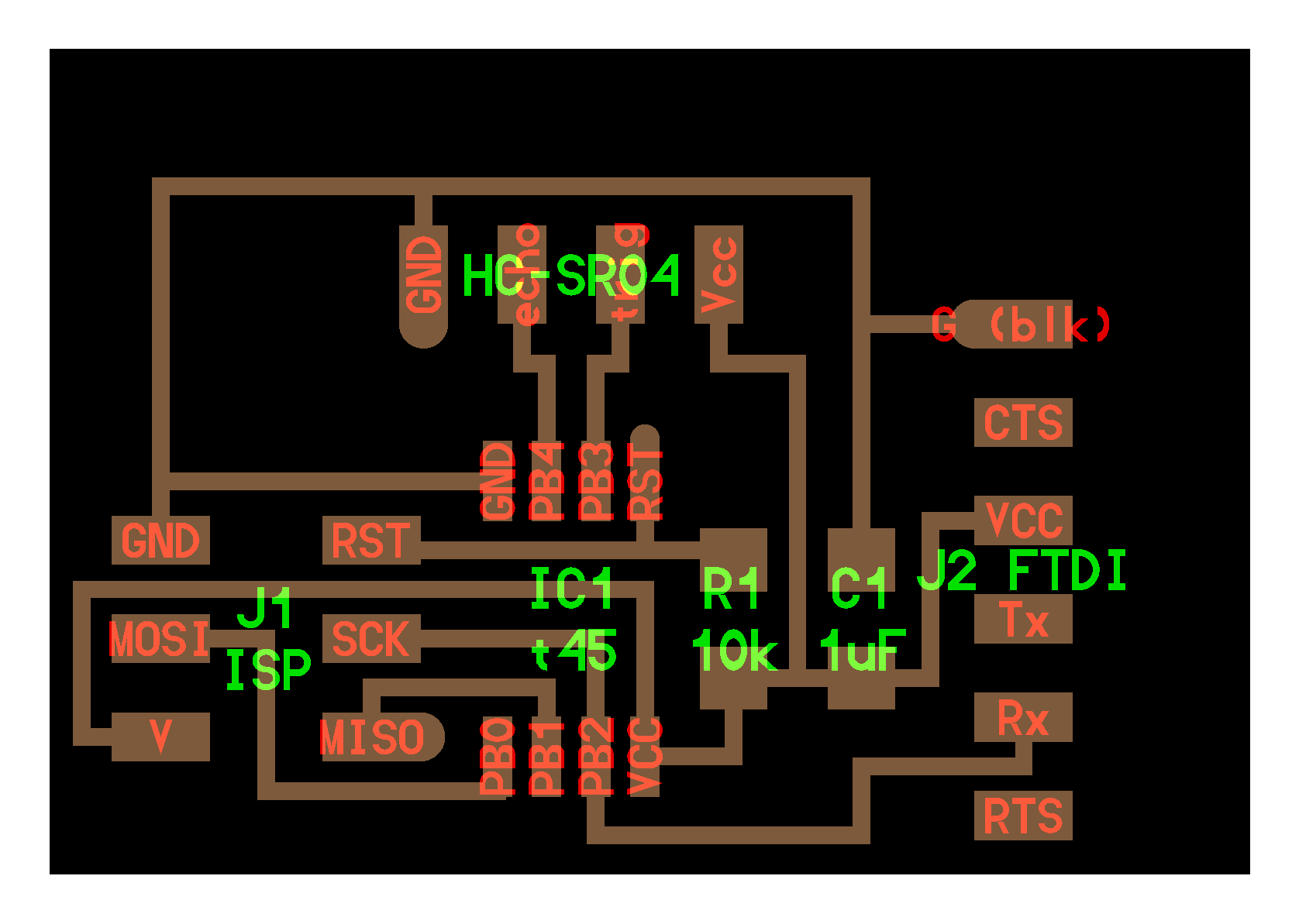
Initially I had refered the board designed by Neil, which was supported by Attiny 45 as seen here
But later I realised that I needed a few pin outs extra for wired communication, which I was unable to in the attiny 45.
Hence I decided to change the processor to attiny 44.
For this I generated the schematic in Eagle refering to the Data Sheet, for the placement of the pins.
As seen here..
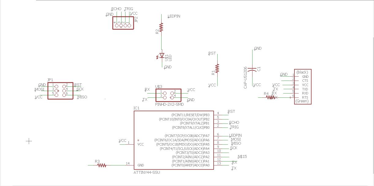
Then I went on to routing this board, it went pretty well, I had auto routed the board.
Then after I realised that the track width chosen by the auto route was 0.010 inches, which was physically difficult to be milled by the bit that we had(1/64").
The issue basically was the track width would have been so thin that it might even have ripped the traces off, hence I used the change command to render the track width to 0.016", for this I had to adjust a few connections manually in order to keep a particular space for the bit to move.
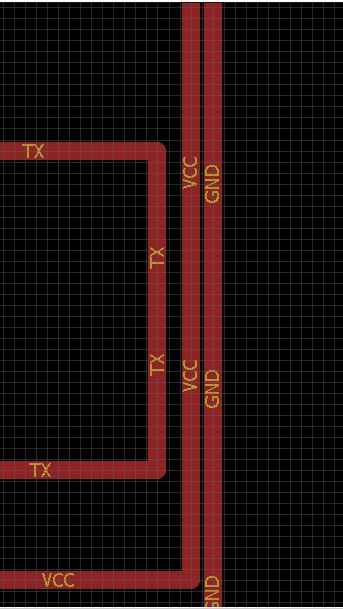
Hence following was the board that I had got out of it.
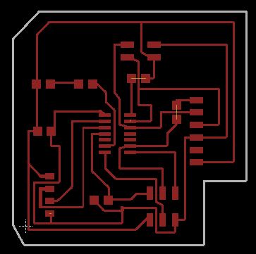
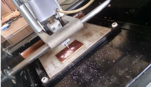
Following the routing I milled the board on the Modella M20X,using the procedure described here
This time I had got a very satisfactory results because there was not bur on the board as was seen before and the tracKs were pretty clean.
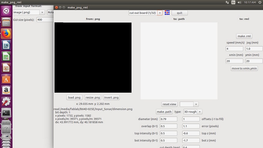
For this I had thought the issue migh be of the width of the dimension so I changed it to 0.016 from eagle and tried making the path again, it worked..
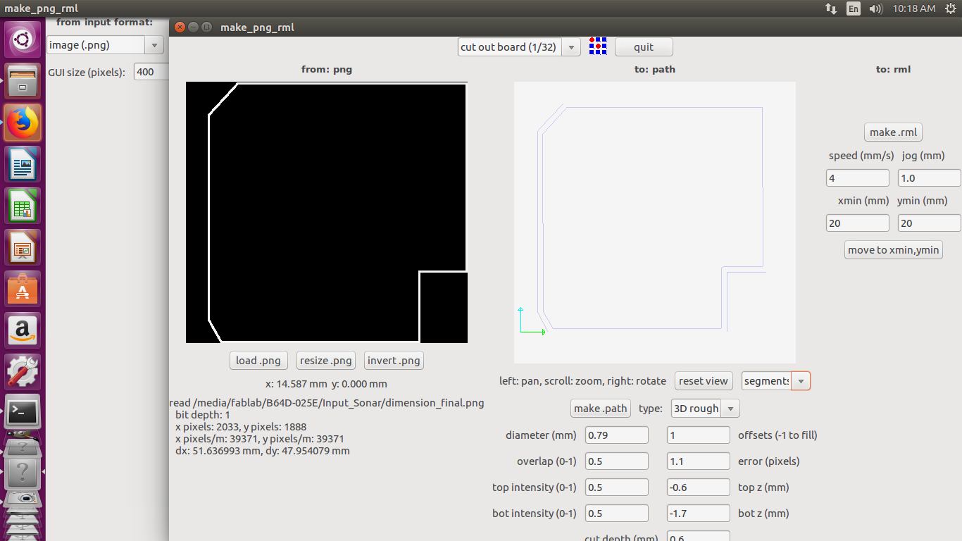
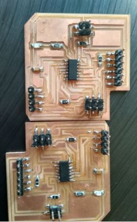
Hence this was the final board I had recieved..
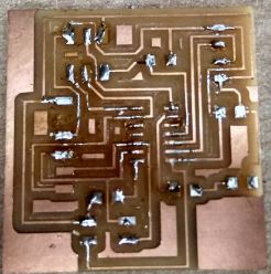
Later step was to solder the board, this time I had imagined it to be quite easy and so it was, the IC had taken very few mins to solder.
The biggest nuisance was made by the 1*6 pin headers, it was becasuse the header that we had were the through hole component that we had bent and were attempting to solder,
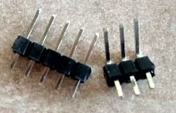
In that process i had initally broken the pin header into 1*3, but thought it would be soldered individually so I did solder the first part, but then realised that the header was misaligned and had to be removed, in the process I actually lost a track of my board so I had to mill it again.
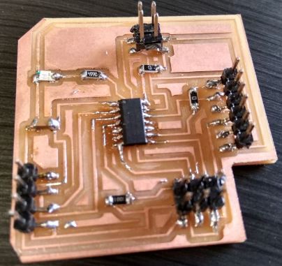
Finally after I soldering the components on to the new board, I had this in by hand...
Task 4:
Programming the board
Programing the board was a but frsutrating cause I hade recieved a few errors such as invalid device signature, which I realised was a very random issue where it could have been the issue with the soldering, or the connections between programmer and the board, or a few more..
After a night of debugging in possible ways, I decided to mill and solder a new , which for no valid reasons again worked in the first go
Hence right after this when I did set to program this was the satisfactory result I got, I was able to burn the boot loader at 1Mhz (internal crystal)
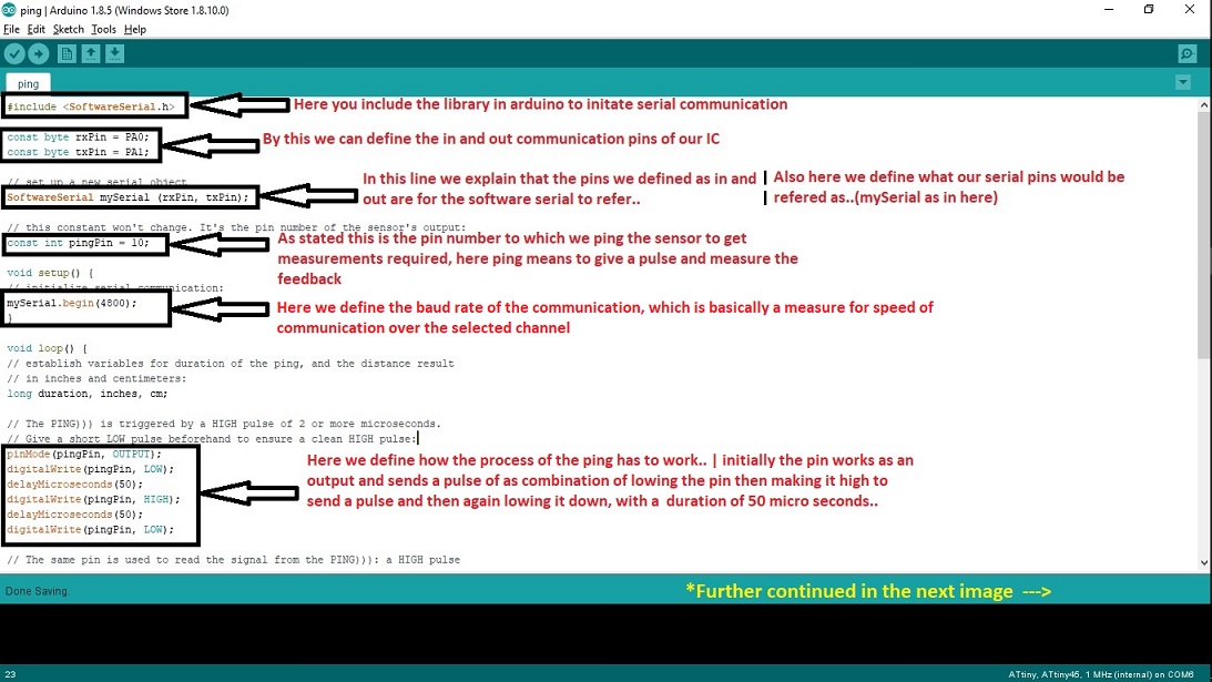
After that I tried to load the "ping" code from the examples of arduino, but there was an error in compiling the sketch , it said that the serial was never defined, so I went through a tutorial, which helped me understand how to add and use the softwareSerial library...
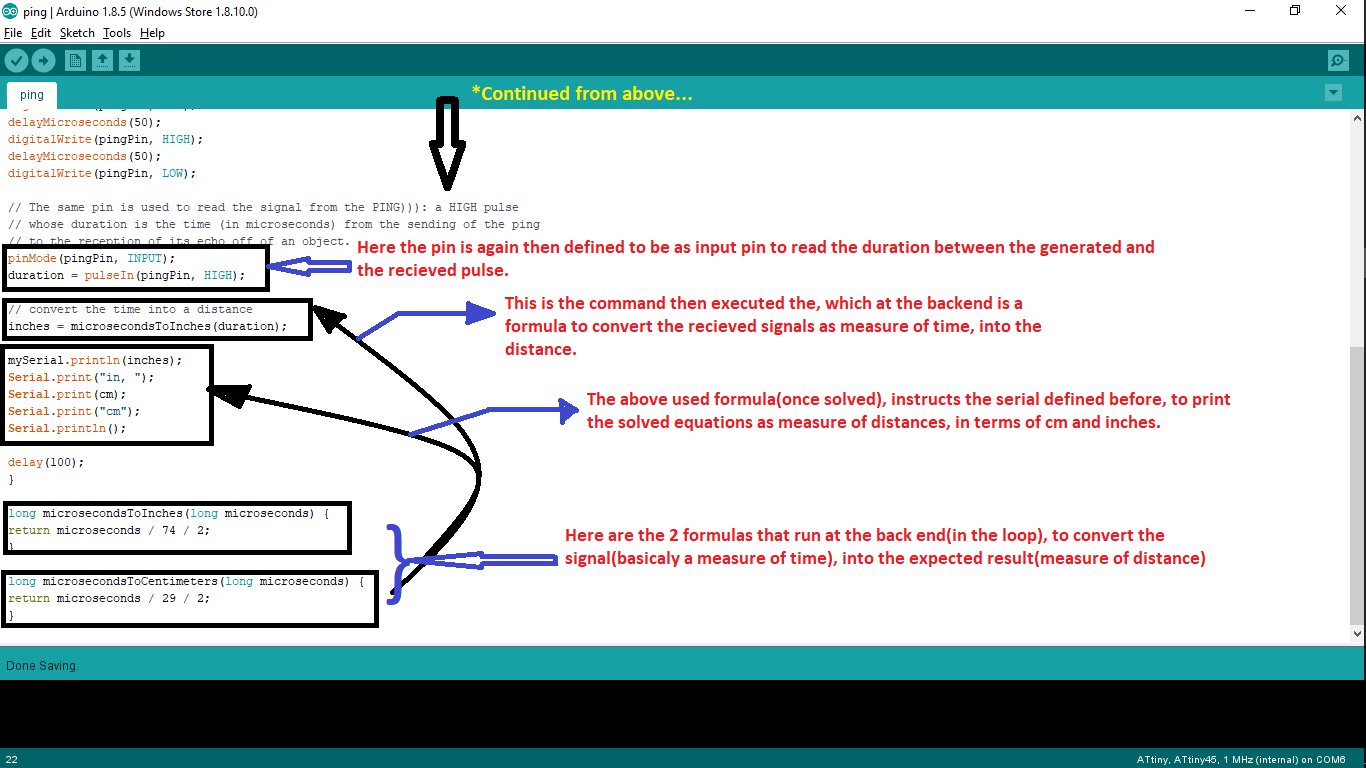
Hence this was my final compiled code:-
Segments of which could be understood here, that would result into analysing what the program does..
Which when I burned I got the following results..
These were the ones seen using the adruino as a power source, and using its RX and TX pins for communication...
After which I also took the result using the FTDI cable as seen here...