WEEK 4: ELECTRONICS PRODUCTION
Objectives
Group assignment:Have I...?
Preparing the trace
The first thing I did was choose my destiny: the programmer I would like to create. After looking at all the available ones, I decided to a ATtiny44 by Ali, the FabOptimus2. So I downloaded images for traces and outlines by the page linked before. From these files I created other ones which can be read by the machine. For make it real I went to mods.cba.mit.edu/. I clicked onPrograms - Open server program - Roland SM-20 (PCB), the code of my Lab's machine. Than Modules - Open server module - File (save). With this passage I created every modules I need. At this point, I disconnected the "WebSocket device" module from "Roland SRM-20 milling machine" one by clicking both of them in the yellow rectangle and then I deleted it. In its place I connected the new "file - save" module.

Than I open my .png traces file clicking on
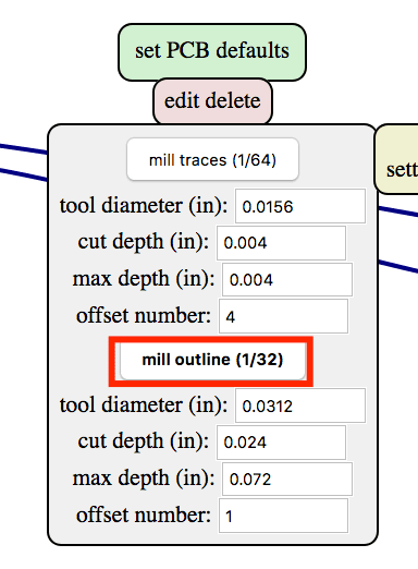
select png file. In the second module I selected mill traces 1/64 (the size of the tip to make traces). In Roland SM-20 milling machine, under "origin" I set X:0, Y:0 and Z:0.
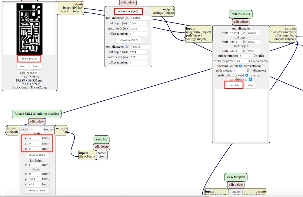
After clicking on
calculate under mill raster 2D module, the system gave me the chance to download the file for the Roland milling machine (with .rml extension).
I repeated same steps also for Outlines.png, but now I selected
mill traces 1/32 (the size of the tip to cut).
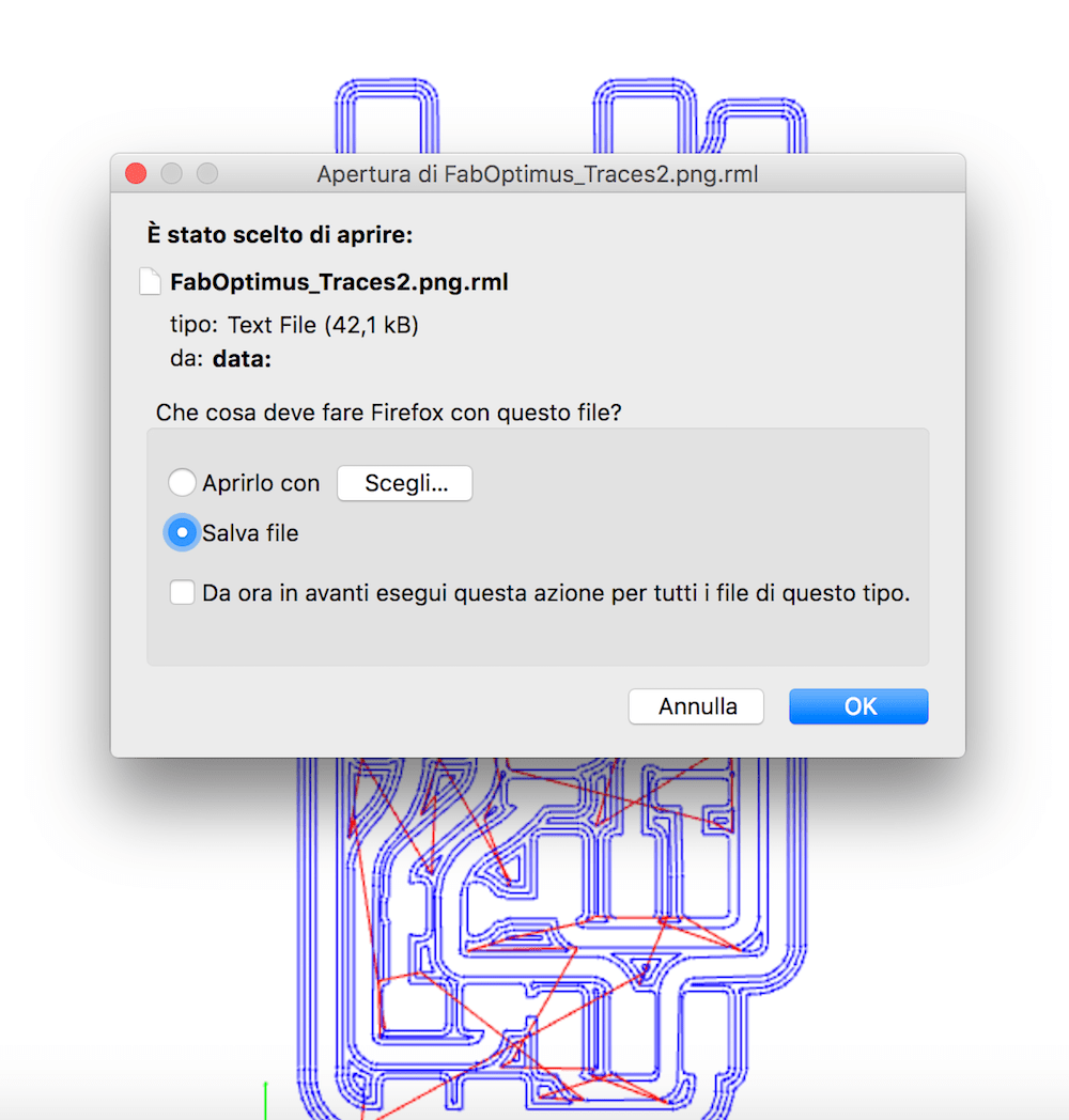
Than I copied my two .rml files in a USB pen drive and I trasnfered them into the PC connected to the Roland milling machine.
---> Download FabOptimus2.zip (including 2 PNG and 2 RML files) (46 KB)
Software parameters
The software to control the machine is VPanel for SRM-20. In this panel, the most important things are: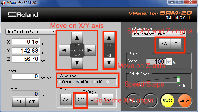
The only things I did in this passage is copying .rml files that I created on the PC.
Setting the machine
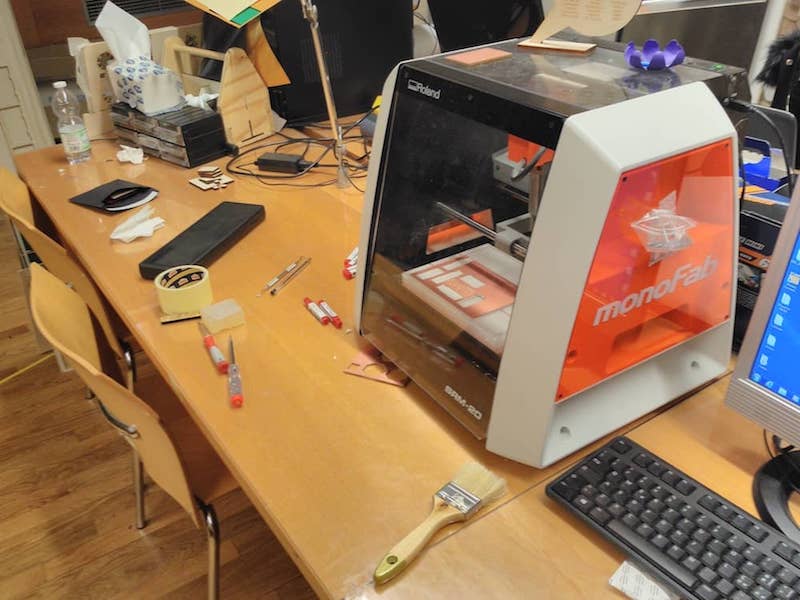
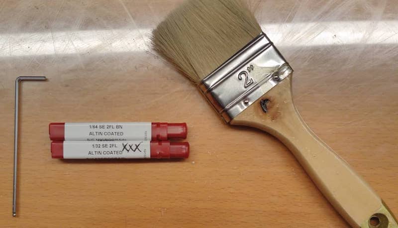
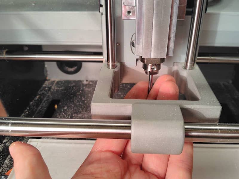
Once I cleaned the plate with a soft brush, I placed the 1/64 inch tip into its housing by tightening it with its tool. Than I placed also the copper plate, by attaching it to the top with a double-sided tape. It's a very important step because during milling the plate, if it is not properly welded, it could literally splash away from its position.
Now I had to place the cutter in the starting position on the X and Y axes from which to start cutting. I moved the tip with software's buttons and, when I found a point that satisfied me, I set it as the origin for these two axes. I did the same thing for the Z-axis tip, calibrating it so that it touched the copper plate slightly.
Only now I I could press
Cut. In the other menu, first of all I clicked on Delete All to clean the file list and than I add my traces.rml file clicking on Add. Finally I clicked on Output to start the cut traces.
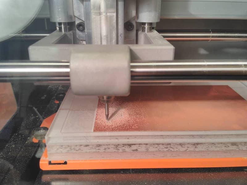
Once it finisched I switched to the 1/32 inch tip, I recalibrate the Z-axis origin, I selected the Outlines file and I started the second cut.
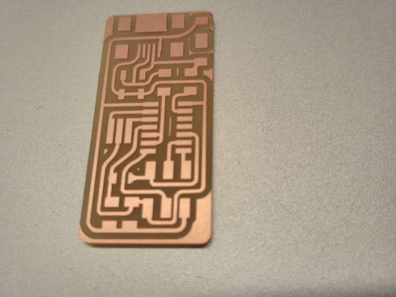
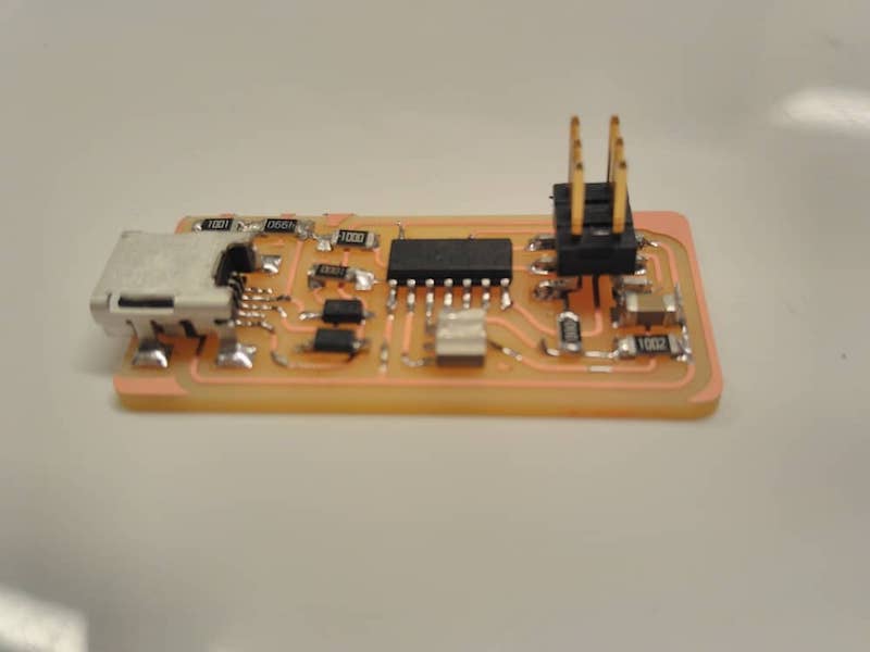
My board
And than, finally, the result!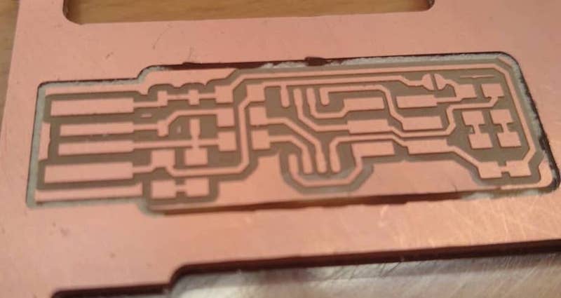
...or not!
This is result of my first cut but even the less experienced have noticed obvious problems.
So, with correct parameters and a second cut:
Soldering
Well...I can say that soldering is not my natural vocation, especially for such small objects. But we are here for learning and soldering is something that can only be learned by practicing it.Before starting, I take 5 minutes to the BOM (Bill of Materials), with the list of components provided in the same board documentation. It's a useful method, especially the first times, because it allows you to have everything at your fingertips.
A bill of materials or product structure (sometimes bill of material, BOM or associated list) is a list of the raw materials, sub-assemblies, intermediate assemblies, sub-components, parts and the quantities of each needed to manufacture an end product. Via Wikipedia.

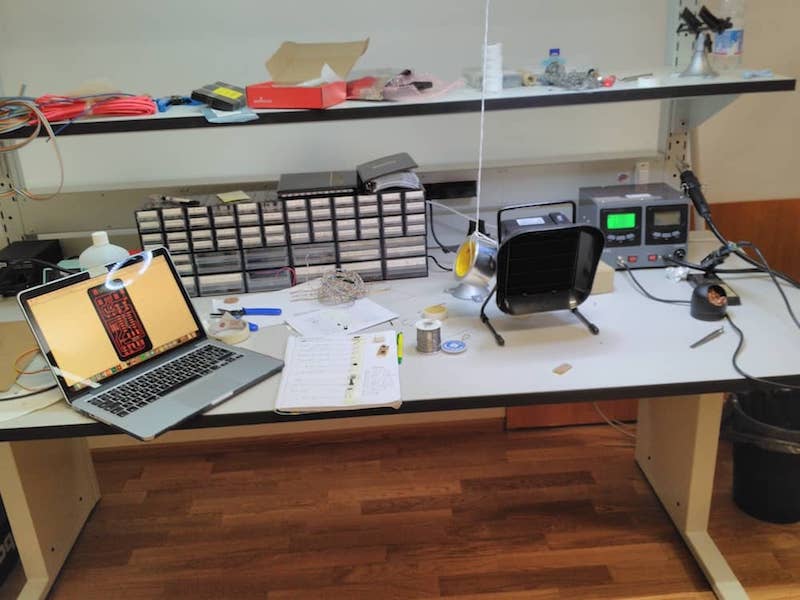
So I sat down at the soldering station and started "dancing".
Always having the image of the board in front of me, I proceeded to soldering the components in the following order:
After a couple of hours (and many, many, MANY bad words), there is the result

***Tips for the future: I recommend to start with the microcontroller, then all the smaller components, then ISP and finally USB. The reason is because the microcontroller is placed in a central position and the pins are very small, so soldering with other components fastened around can be a little bit more complicated.
Programming
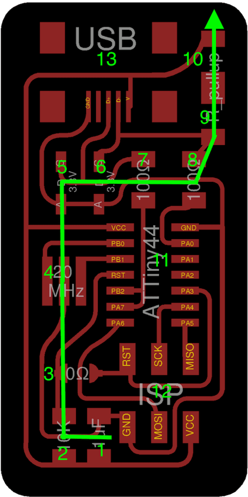
And than...the moment of truth!I connected my board to another one, previuosly programmed by my Lab as a programmer. In this way I could program my board to make it a programmer too. As first thing, I had to connect boards together with a SPI cable.
Boards must be in the same direction!!! In this way the cable can connect same pins together (for example, the GND with GND etc...)So I connected my board to the programmer with this SPI cable and the programmer to my laptop. I created a sort of bridge to allow the communication between computer and my board.
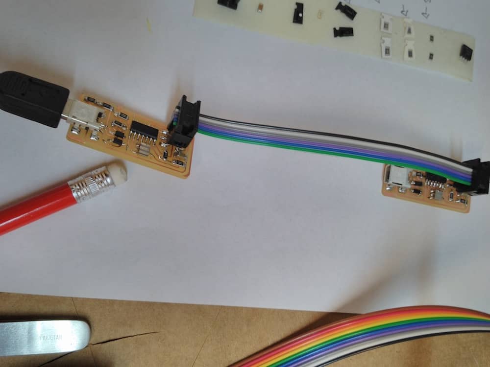
So I went to FabISP: Programming tutorial and I followed the instruction for my OS (MacOS). I'll try to simplify steps if you also want to program a FabOptimus on a Mac.
-->Step 1: Softwares
Basically I had to install:When I downloaded/installed everithing, I copied the
fabISP_mac.0.8.2_firmware.zip to my Desktop and I extracted the archive simply clicked with the right mouse button.
Tutorial makes this passage via terminal, renaming the folder as "firmware". I leaved the folder name unchanged. Basically it is the same, but you have to remember to tap "fabISP_mac.0.8.2_firmware" instead of "firmware" when you write commands on Terminal.As last passage, I modified the
Makefile file contained inside the firmware folder. I opened with TextEdit and I commented:
#AVRDUDE = avrdude -c usbtiny -p $(DEVICE) # edit this line for your programmer


          AVRDUDE = avrdude -c avrisp2 -P usb -p $(DEVICE) # edit this line for your programmer
with
AVRDUDE = avrdude -c usbtiny -p $(DEVICE) # edit this line for your programmer


           #AVRDUDE = avrdude -c avrisp2 -P usb -p $(DEVICE) # edit this line for your programmer
Simplify it a lot, in this way basically I am communicating that my board is an USBTiny and not something else.
--->Step 2: Terminal commands
In this part I'm going to write commands for terminal app and not the system's answer too (very long ones!). If you want to know if the system has given you confirmation or errors, please see the official tutorial that I've linked before.I opened Terminal app and I wrote:
cd Desktop/fabISP_mac.0.8.2_firmware
---
make clean
---
make hex
---
make fuse
---
make program
And (fortunately) everithing worked fine!
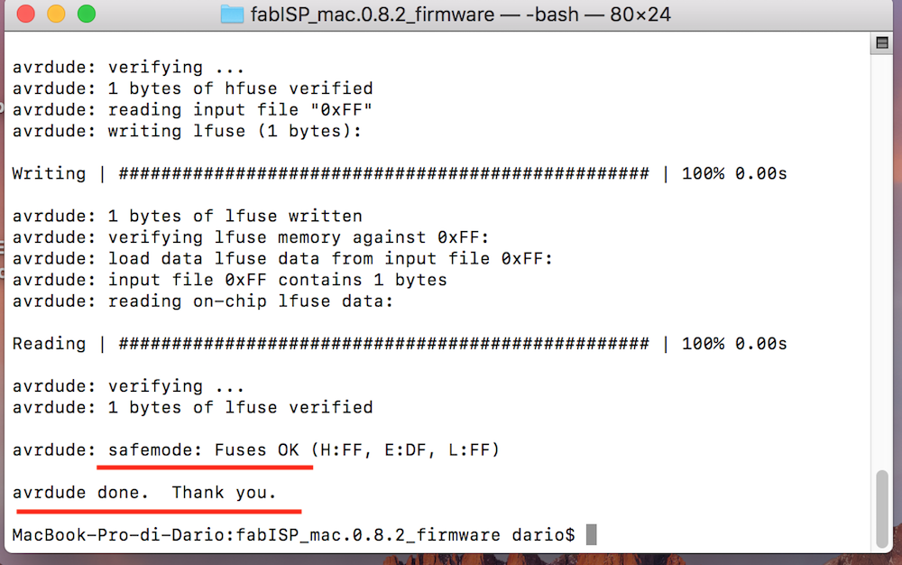
To have a confirmation, I connected my board directly to my laptop via USB and I opened System information. Under USB voice menu I've found FabISP!

--->Step 3: Can my board program other boards?
Now, theoretically, my board become a programmer, so it can program other boards. So I created a second FabOptimus2 board and I have tried the whole procedure again. But when I launched "make fuse" command, I have received an error:
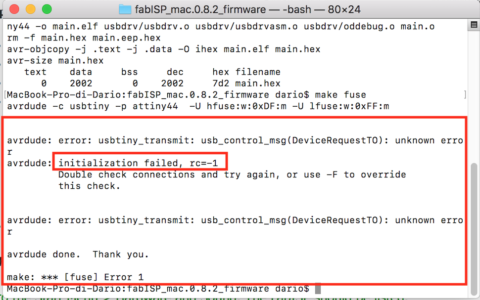
The first thing I thought was: I have definitely welded badly some element (for example those of the microcontroller or USB where traces are very small, damn!). I checked again the welds under the magnifying glass but, except for a couple of them that were not perfectly shiny, I didn't notice other particular critical points.
I then tried to program it with the programmer provided by my lab and in this case everything worked!
So I asked for an opinion to Simone Guercio which advised me to re-read the documentation regarding the board, making me notice the writing:
[...]after you program the board, you must remove the 0Ω resistor [...]So I sat down again at the soldering station and removed the 0Ω resistor (with a lot of difficulty).
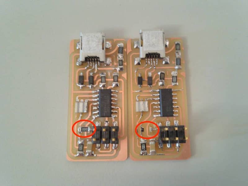
In the end I re-programmed the second board with the first one and now (finally), in this case, the process was completed without errors