Exercise 6. Electronics Design
Assignment: Electronics Design
- Redraw the echo hello-world board, add (at least) a button and LED (with current-limiting resistor), check the design rules, make it (f you have time this week, test it).
- Optional: simulate its operation. Measure its operation
Learning Outcomes
- Select and use software for circuit board design
- Demonstrate workflows used in circuit board design
Evidence
- [x] Show your process using words/images/screenshots
- [x] Explain problems and how you fixed them, including how you worked with design rules for milling (DRC in Eagle and KiCad)
- [x] Include original design files (Eagle, KiCad, Inkscape, .cad -whatever)
Process
The tutorial for this week provides comprehensive steps for workflow, explanation, and BOM. Without any experience designing electronics, I found this to be particularly helpful but only discovered it after I'd starting working on my board layout.
Once I understood what electronic components I needed, I gathered them from our inventory, and set out to design my board!
| Board Component | Purpose |
|---|---|
| ATTiny 44 microcontroller | stores program |
| FTDI Header | provides power from and communication with computer |
| 6-Pin Header | used for programming board |
| 20 MHz Crystal | clock |
| 10k Resistor (2) | pull-up resistor |
| 499ohm Resistor | current-limiting resistor |
| Button | can be used as reset, can be programmed |
| LED | can show if board is powered, can be programmed |
| 1uF Capacitor | stores electrical charge |
Designing
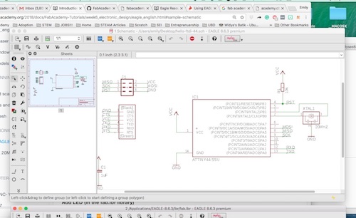
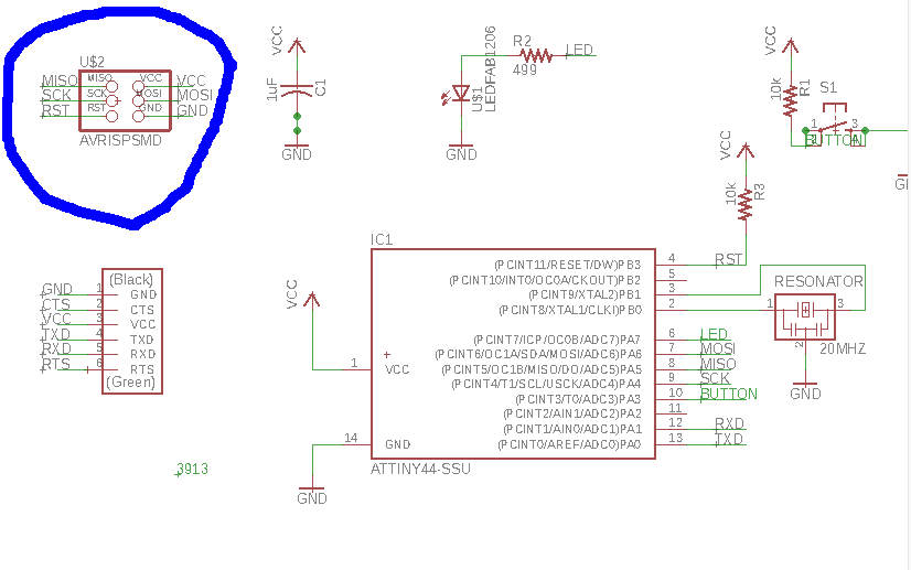
I downloaded Eagle, and the Fab Component Library from this week's tutorial. The files from this week's recitation were helpful in putting together my design, particularly the image of Neil's Hello board.
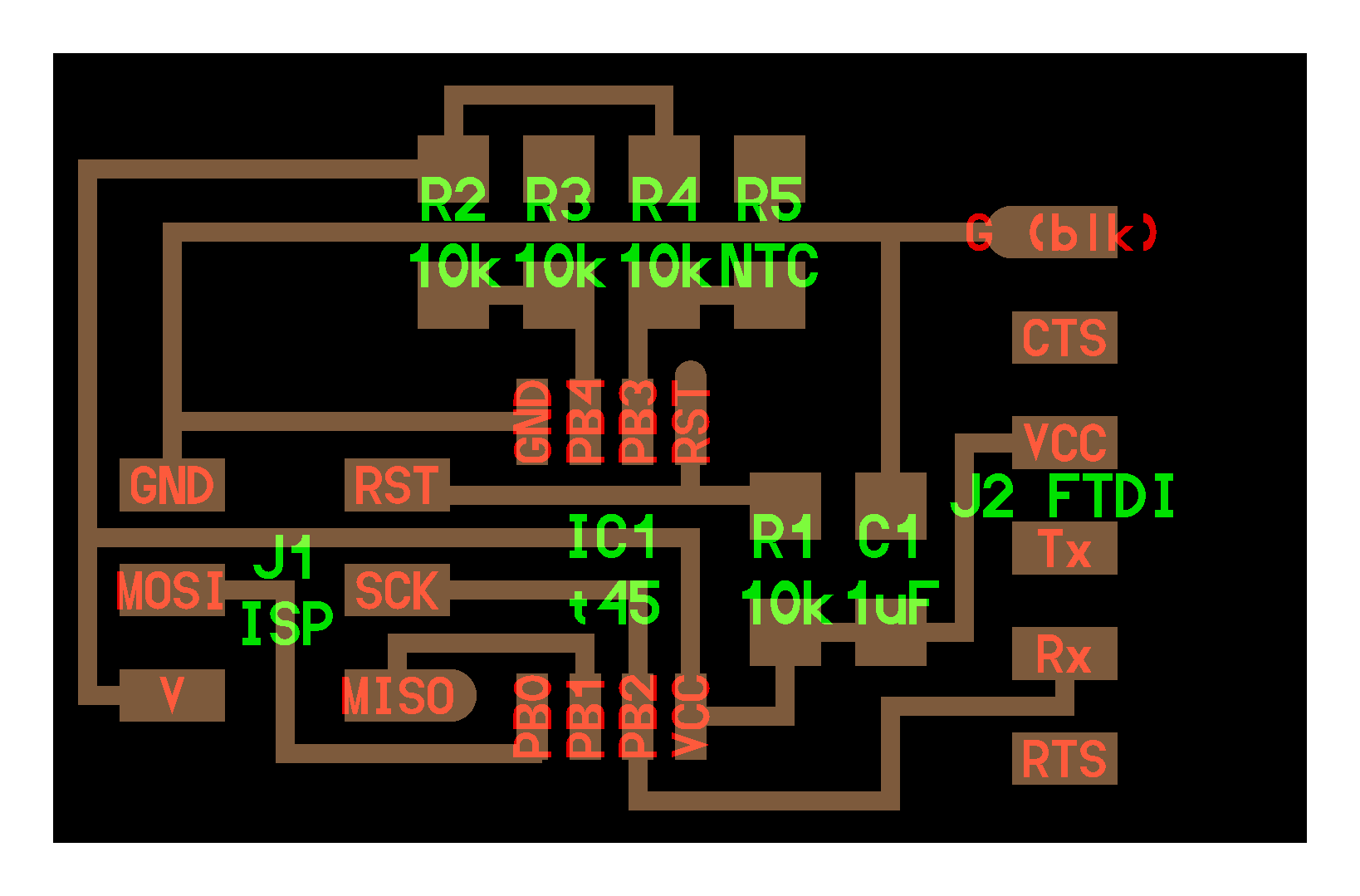
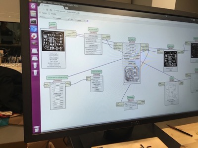
Schematic
After installing the Fab component library, I began putting the components on my board- the physical ones listed previously and the following additions from the tutorial: * Ground (GND) * Power (VCC) * Connect copmonents to the common GND and VCC * Connection between pin 10 and button * Connection between 6 and LED
Create nets to connect components to each other
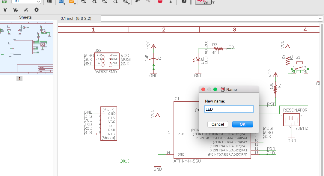
Name various components on the board and add labels using the "text" command
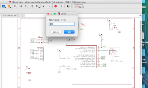
Set values for cystal, resistors, and capacitor
 Set values for cystal, resistors, and capacitor
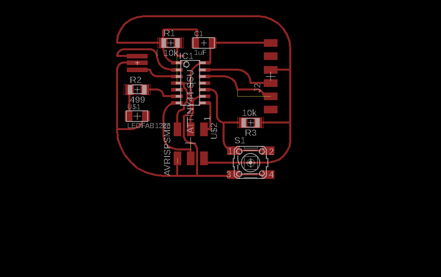
Board Layout
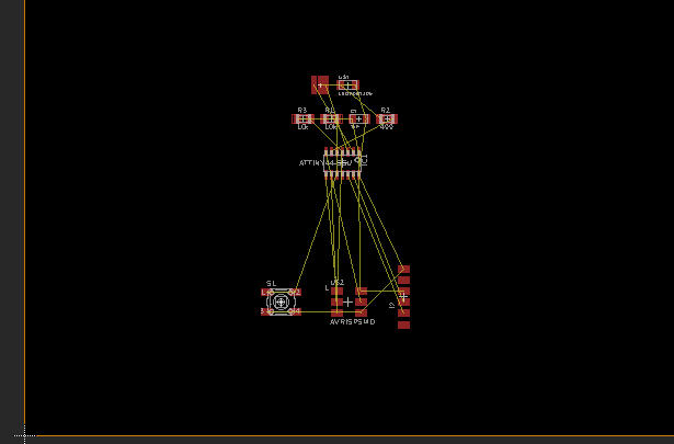
Switching over to the board layout view revealed a mess of yellow unrouted traces.
Looking at the footprint of the 6-pin header, I realized I'd selected the wrong one. In the schematic I went back into the library to replace it with the correct component (AVRISPSMD).
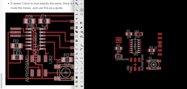
I arranged components using the tutorial as a guide and then changed the yellow unrouted traces to red routed ones. The autorouter didn't prove to be particularly useful for a final layout because traces were very close together, but I did find it helpful to think of multiple ways that components could be connected to each other. I created curving traces for aesthetics and learned later on, in many instances, having 90º traces isn't ideal for functionality of a circuit board.
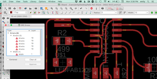
About halfway through routing them I realized the traces were set too thin for the tools I'd be milling with. I didn't find a way to change all of them at once so manually ripped up and changed each trace from 6 to 12 to accommodate a width of at least 0.010". TIP: You can group all the nets and then apply a group operation to change all traces.
With everything routed it was time to check for errors. I downloaded the Fab Design Rules Check file which is adapted for the milling tools in the FabLab. I had a few airwires and some with errors width which I was easily able to resolve.
Checking Design Rule Errors
Finished Board Layout
Converting Board to Image
Exporting from Eagle
In "layers" I show only top, pads, and vias. These are the parts which will be milled. I export this image from Eagle to a .png file making sure the settings are monochrome and 500 DPI.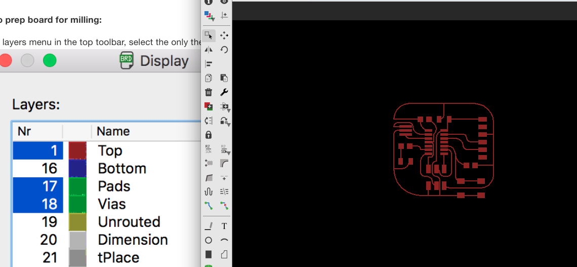
Prepping in Gimp
I opened the image up in Gimp and converted it to greyscale. The Roland will leave the white parts of the image (traces) and mill the black space around them or vice versa depending on the file.
Set canvas size
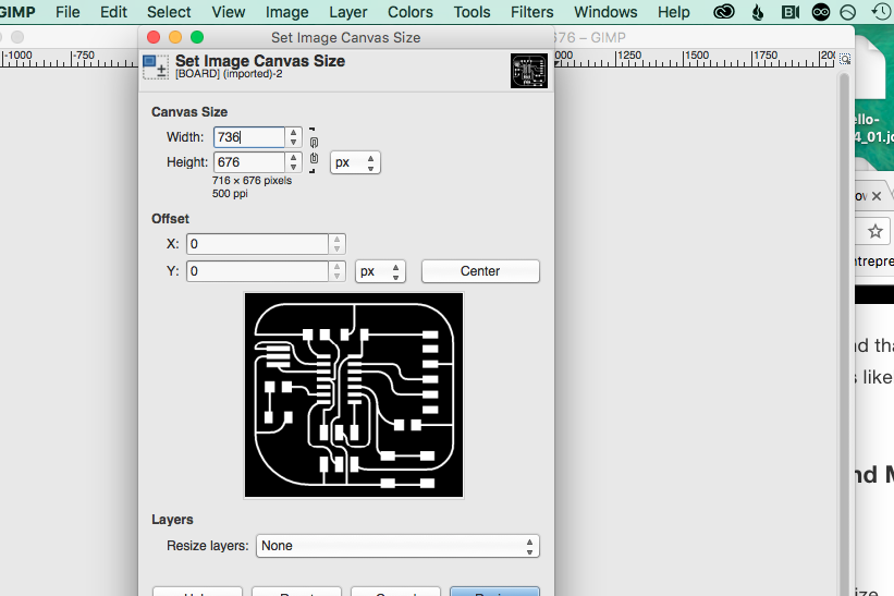
I linked the dimensions and added 20 px to the width to leave space between the board and the exterior cut. I centered the image on the new canvas. Then I flattened the image and added a white border for the interior.
I added a lotus image onto the board and text in Gimp.
Finished Design
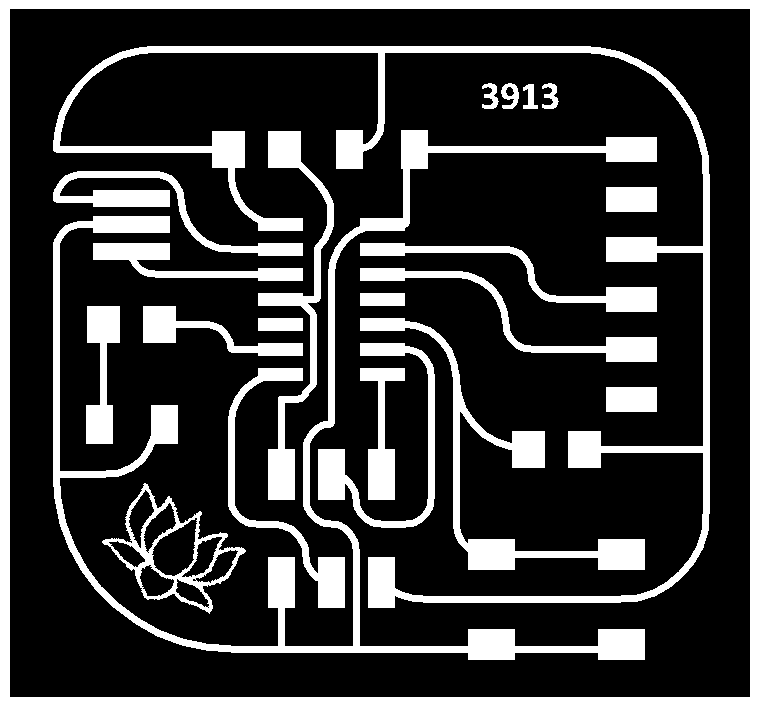
To make the "cut file" for the Roland to mill out the board from the PCB, I inverted the colors and filled in the traces so that only the black border line will be milled out.
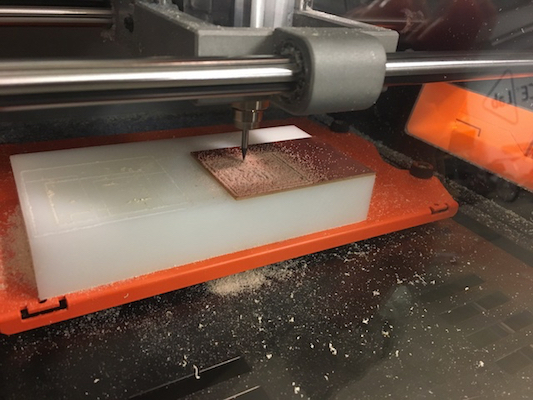
Milling
Armed with my saved files I thought I was ready to mill my board. My colleagues discovered that there is an error in Eagle (still an issue with version 9.0.01) for Mac OS where it doesn't properly scale. As a workaround they discovered that Mac created Eagle files opened up on a non-Mac computer can then be exported as an image in the correct size. With this knowledge I went back to earlier processes before moving forward.
New workflow for PCBs * Create board in Eagle on my Mac * Open file in Eagle on a PC * Export image, invariably I end up manipulating it on my personal computer * Bring Gimp file into Mods on our Ubunto/Windows computer running the Roland
The Roland SRM-20 sometimes seemed to get 😖 and needed to be reset. What I thought would be a quick cut job took some time between resetting the machine, resetting the x,y,z and sometimes having to restart Mods.
Using Mods
Milling Traces
Finished milling, time to vacuum
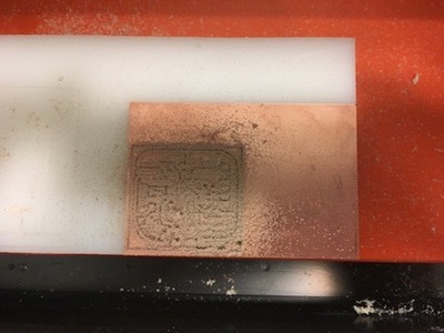
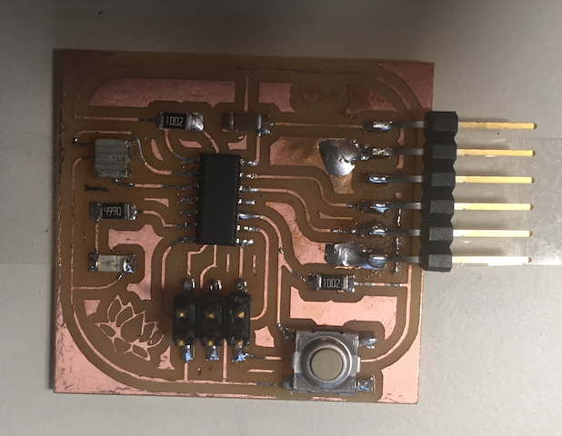
The numbers I'd added as text in Gimp were too small for my tool but the lotus flower milled nicely!
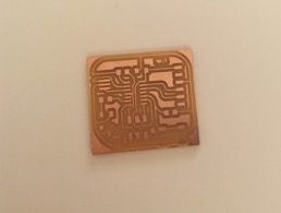
Milled board
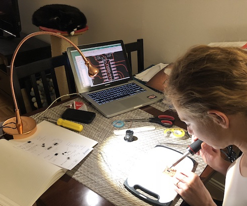
Stuffing
Soldering Components
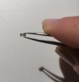
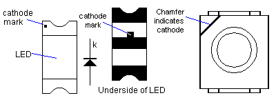
LEDs have polarity. Before soldering you need to check the board layout file and LED component to ensure they are oriented correctly on the board.
I ripped up a trace on the 6-pin header which needed some careful attention before reattaching
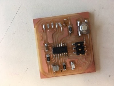
Finished board
Testing
Using multimeter to ensure that traces are connected properly.
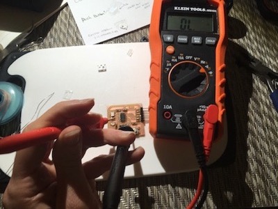
In addition to testing my board, I was able to program it- the temptation to have it "do something" was too strong to resist! More on this here in Exercise 8.
Files
Eagle files: Schematic, Board Monochrome Gimp files for milling: Traces Interior