Exercise 06 - Electronics Design
Weekly Assignment
Group Project:
Individual Project:
Group Assignment
The group assignment is to test out the equipment in our lab that is used to troubleshoot and observe the operation of our PCBs. We used multi-meters and an oscilloscope. We are still in the process of finding an appropriate bench top power supply, we hope to borrow one from the physics department for testing purposes and then order one when we decide what type and style we want. I am very familiar with multi-meters as a physics teacher but had less familiarity with an oscilloscope. Off to find a tutorial!
A great YouTube video on the basics of oscilloscopes
We decided to test our oscilloscope while "following along" with the above tutorial. The following is a list of things we learned about the 'scope, how to use it, how to fine tune the readout, etc.
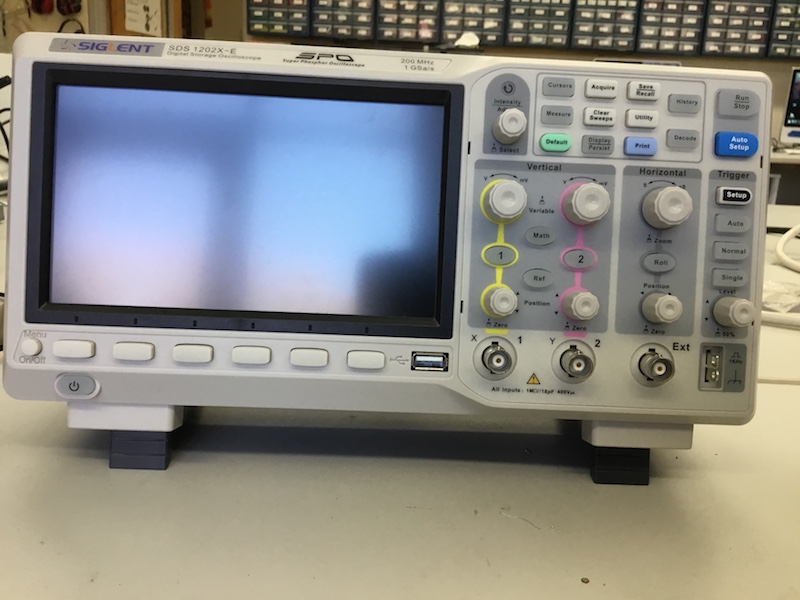
Our oscilloscope is very similar to the one in the tutorial!
- The oscilloscope essentially creates a Voltage vs. Time graph when hooked up over a potential difference
- The probe should be plugged into Channel 1, which should be turned "on". Nothing is plugged into Channel 2, which should stay "off".
- Generally, you want your probe set to 10X, which does NOT amplify your signal ten times, but helps attenuate it while still not affecting the circuit you are trying to measure
- The other menu settings should be as follows: Type- Edge, Source-CH1, Slope-Rising, Holdoff-Close, Coupling-DC, Noise Reject-Off
- The probe should be calibrated at least once a week by plugging the ground clip and the probe tip into the built in frequency generator. This one is a 1 kilohertz square wave generator.
- Other adjustments that need to be made include adjusting the vertical and horizontal scales so that the wave form is visible on the monitor, adjusting the trigger level to have it to start measuring on a rising edge, and tuning the compensation capacitor to level off the square wave forms
- You can click "Run/stop" to freeze the wave form and allow you to take measurements off of it
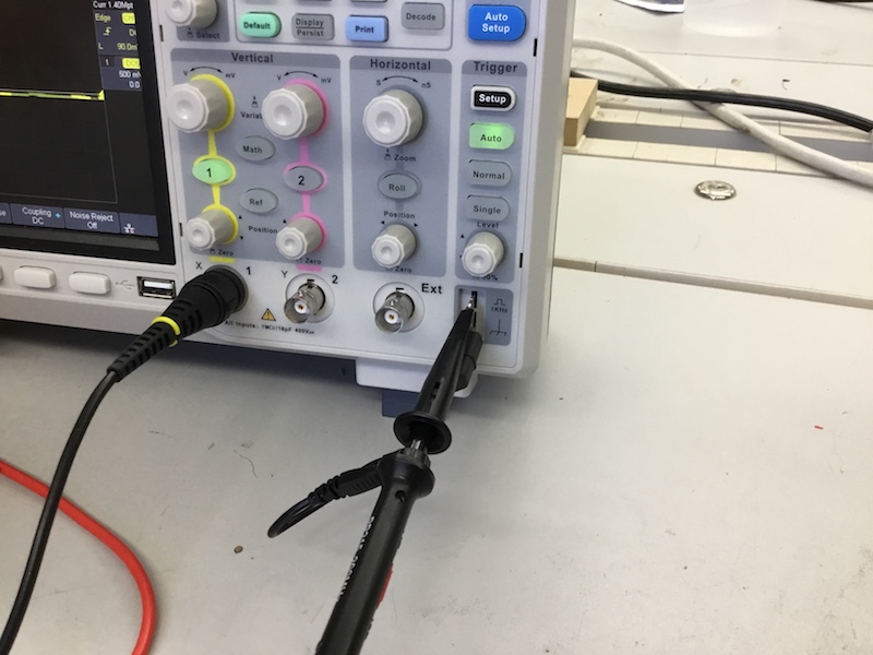
The probe plugged into the frequency generator for calibrating
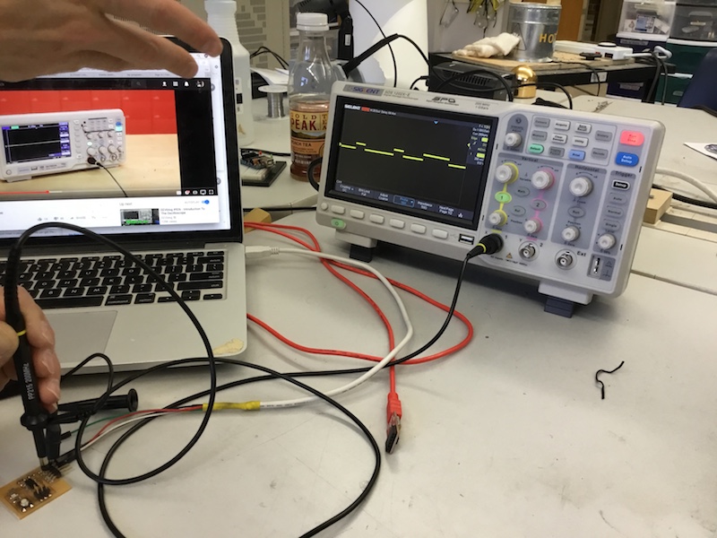
Testing one of our programmers
Finally, we have a short video of using the oscilloscope
Individual Assignment: Redraw Echo hello world board, add a button and LED, check design rules, make, and test
Tinkercad Circuits
Someone in our Lab who had done FabAcademy several years ago suggested I start out designing my PCB with Tinkercad. I was skeptical, as I had rarely used it and thought it was not 'sophisticated' enough. Nevertheless, I loaded it up and gave it a try. I didn't really care for the picture style interface and the drag-and-drop nature of the designing. Also, I quickly realized that I could not load the Fabacademy component library into Tinkercad. I could not easily find all the components I needed in the Tinkercad interface and overall it felt very clunky and difficult to use because I was being forced to manipulate things the way they wanted me to, not necessarily how I wanted to do it. I gave up on this about an hour in and decided to move on to Eagle.
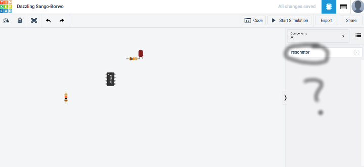
No resonator found along with several other components
PCB Design with Eagle
This week was VERY hard for me and I am not sure why. I was pretty confident going in - I watched the lecture class earlier than normal, I borrowed a couple books from the FabLab, and I did a lot of reading and working over the weekend. I felt like I was ahead of the game. (Spoiler alert: I was not.) I read chapters 1, 2, 4, and 5 in this book and started designing my PCB in Eagle.
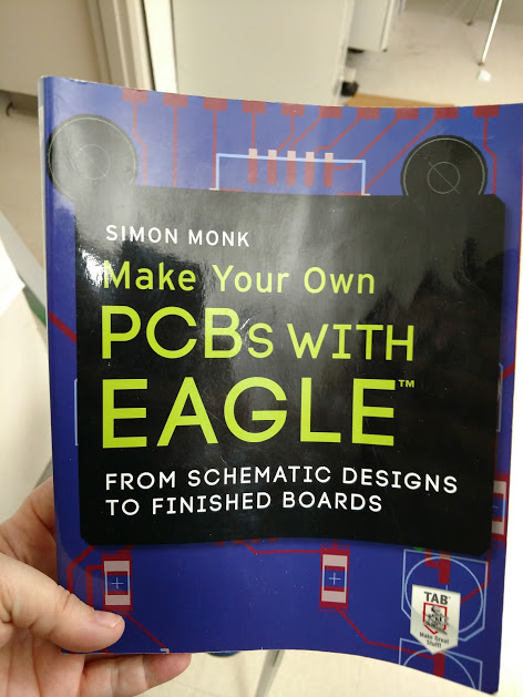
The book I read, which was very helpful
I ended up designing multiple schematics, several boards, milling at least 3 PCBs, and soldering and re-soldering the board I ended up using. The finalized general process I settled on was:
- Create new schematic
- Add components to Eagle schematic
- Arrange components roughly where I want them to be
- Draw nets between components
- Do an Error Check
- File > Switch to board
- Move components around to minimize the "ratsnest"
- Use the "route" tool to create the traces between components on the board (use "rip up" tool if you need to remove a route, delete does not work)
- Do a Design Rules Check
- Once you have routed the traces, turn off all layers except top. Go to "File > Export as image" and choose the following properties: monochrome, .png filetype
- Load the just created .png file into Fab Modules and follow the same procedure for milling on the Othermill as I discussed in Exercise 04 - Electronics Production
Specific Screenshots of My Process
So, following along with the examples from the book, I was able to make the schematic somewhat easily in Eagle. My familiarity with Fusion 360 also helped while using Eagle.
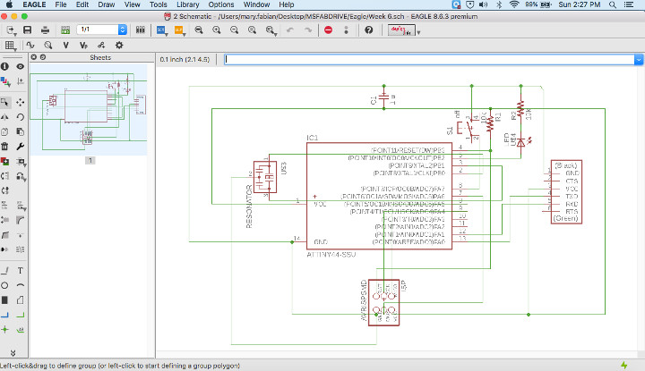
My first schematic
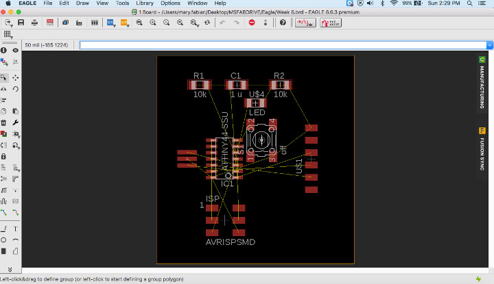
The board associated with the first schematic
All seemed to be going really well, so I kept going. The next step was to route the traces in Eagle. This is where things started going south. I decided to try the autorouter in Eagle. I tried different optimizations, and kept getting boards with vias. Why??
So many vias and I don't know why
FINALLY, I realized that when I was clicking the autorouter, I needed to turn off the bottom layer when I was autorouting and it finally stopped giving me vias.
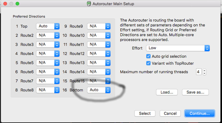
Set this to N/A and it will only give you a top layer PCB route
One of the optimizations from the auto-routing
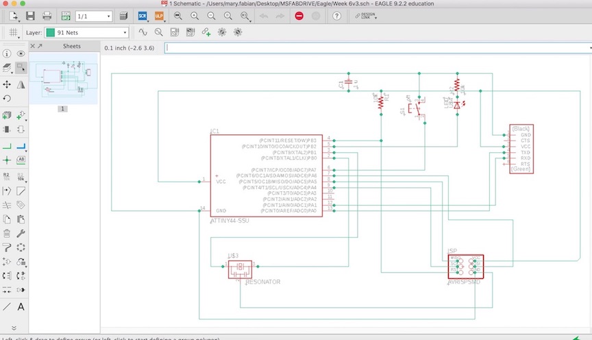
My final schematic. It's labeled version 3 but I think it's actually much more than that.
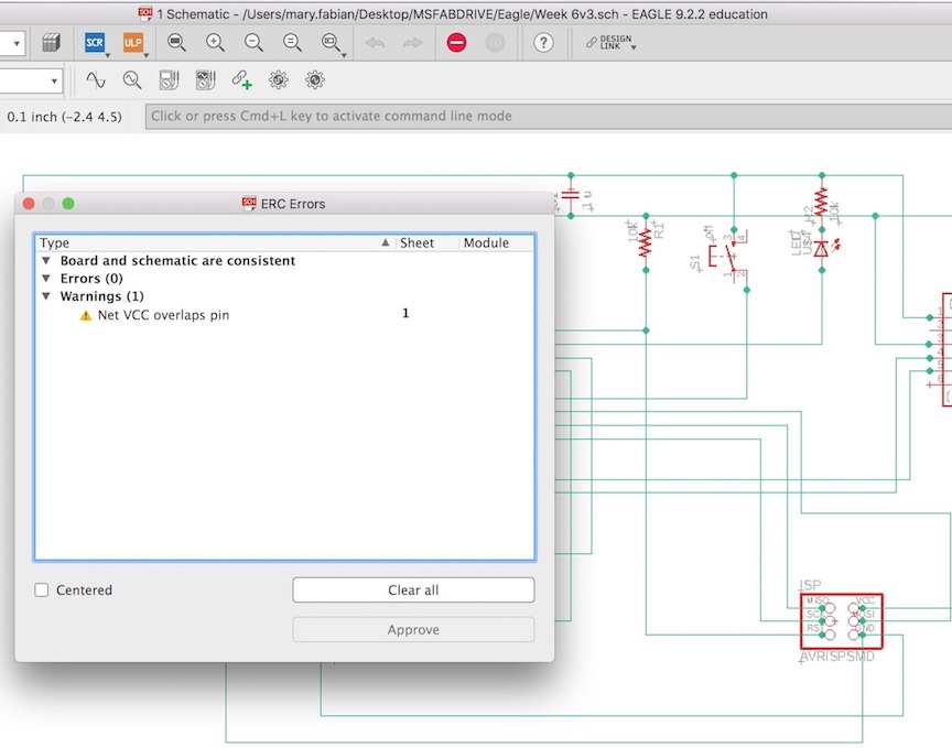
Here is a screenshot of the schematic after I ran an error check. No errors! Just one warning that I can safely ignore.
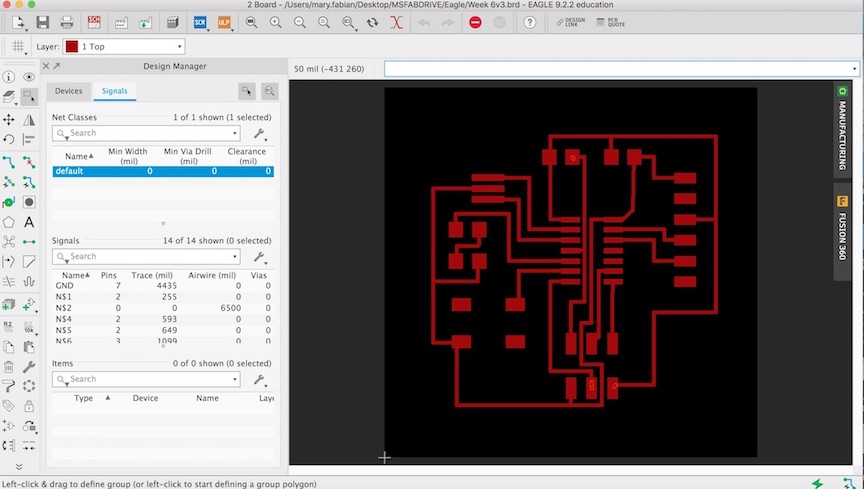
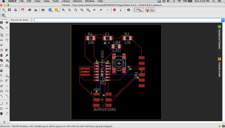
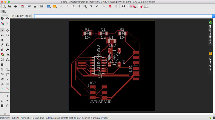
The matching board for the final schematic
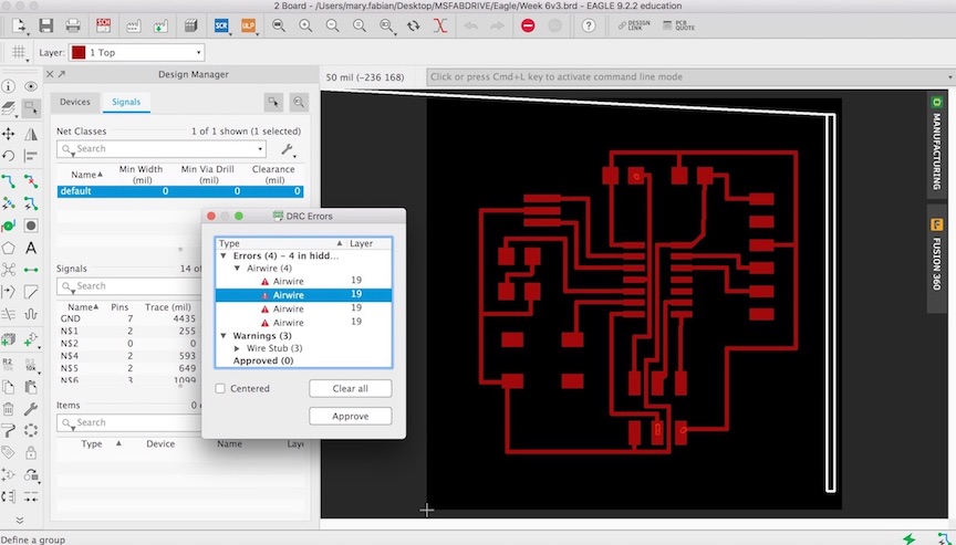
The final board with a design rules check. The "airwire" error is hidden and related to the border that I added to the file so that our Othermill would do a nice cut of the outside of the board and I wouldn't have to. This, too, can safely be ignored.
I quickly realized that the auto-routing was not everything it was cracked up to be, but I still decided to keep trying. I was going to try to mill one of these auto-routed options even though none of them looked particularly "do-able". I figured out I needed to export the board as an image (.png) if I wanted to use FabModules. The best way to do that was to turn off every layer except the top layer which held the traces and pads and set it to "monochrome". You will then end up with a black and white .png file that you can use with FabModules.
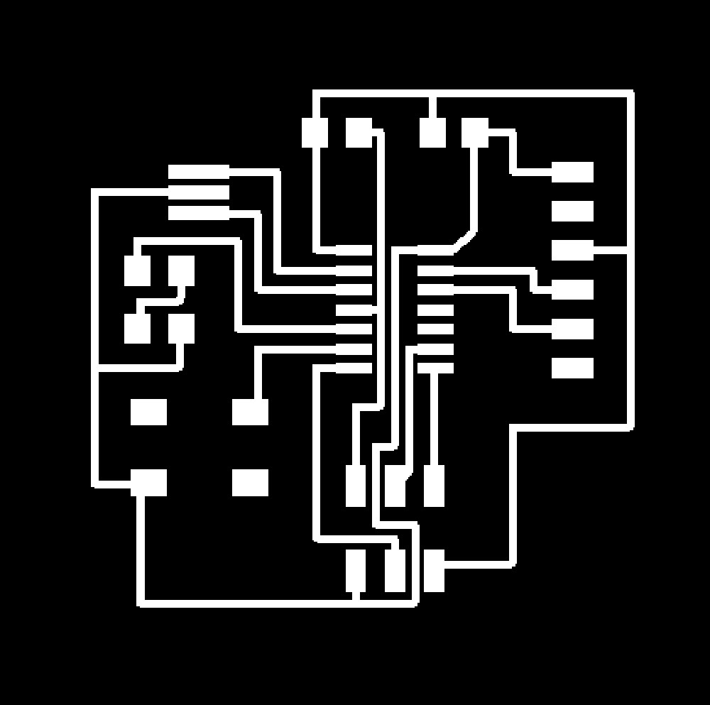
An example of a .png file to be loaded into FabModules (right click to download)
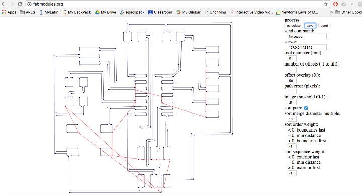
Loaded into Fabmodules and ready to go
I am listing all of my design files from Eagle here, so if anyone would like to download them, feel free.
- Final Version of my Schematic (.sch file)
- Final Version of my Board (.brd file)
- Final Version for Cutting (.dxf file)
Making and Testing the Board
I followed my procedure from Exercise 04 - Electronics Production. I milled one board and thought it looked like the traces were too close together and there was very little separation between the traces and the surrounding copper. I worried a lot about bridging gaps with a sloppy solder and so I decided to make a new, more spread out board. I later came to realize that the tiny traces were because I had chosen poor values in FabModules, using an offset of 1 instead of a more reasonable value, like 4. Next time I will know to choose my offset better and not have to do all this extra work!
The first attempt with the traces and the surrounding copper VERY close together
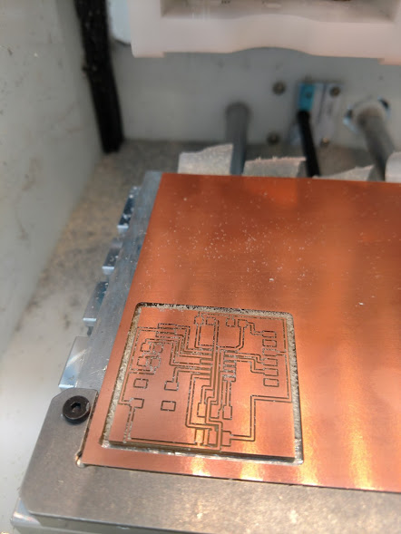
The second board with the traces more spread out and separated from the surrounding copper
I still had concerns about my relative inability to solder such tiny pads and traces without accidentally bridging the gap to the surrounding copper, so I decided to make ONE MORE board where I would mill out the surrounding copper and be left with only the traces and pads. I did this by importing my Eagle design into Fusion 360, taking the traces image and placing it onto an extruded surface. I generated contour and pocket toolpaths that would mill away all the internal and external copper bits, leaving only the traces and pads behind. This ended up working REALLY well, but possibly being a bit overkill. I really liked the way it ended up, though.
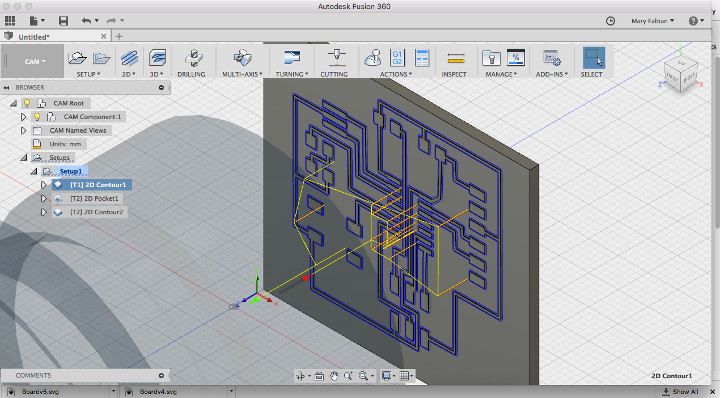
The Fusion 360 file ready to be milled
I then took the Fusion 360 design file and loaded it into Othermill and set it to mill the board. Between all the traces, pocketing and contouring, it took almost 30 minutes.
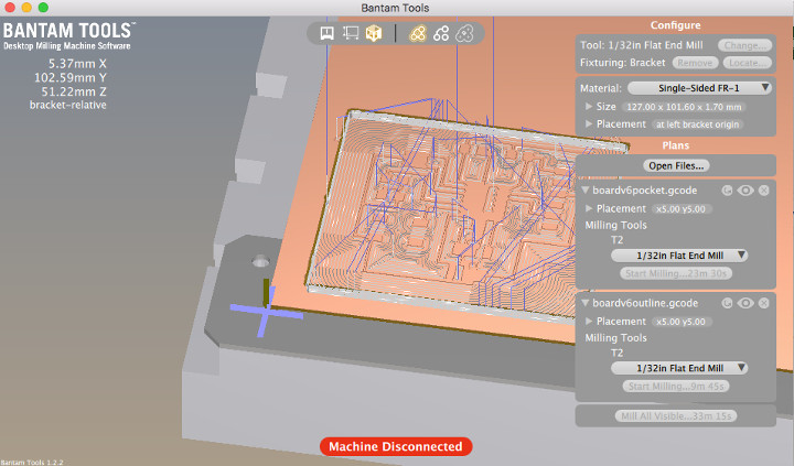
The toolpaths on the OtherMill
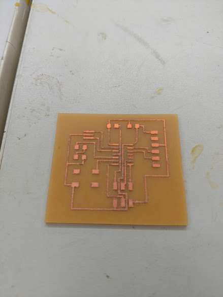
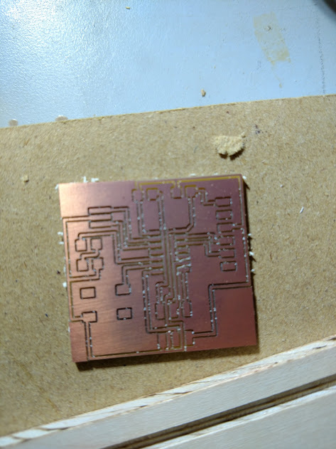
The overly milled board pre-soldering
It was time to solder. My labmate, Will, had already pulled all of the pieces so all I had to do was place them and solder. This actually went relatively, almost alarmingly, well and quickly. It looked really good, but was everything aligned correctly? Would it work??
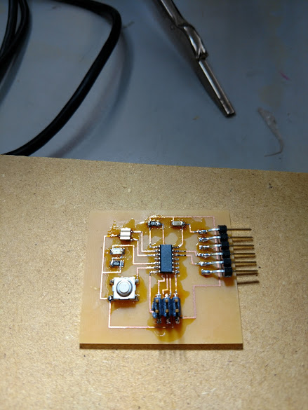
The components soldered into place
It was now time to test the board after ALL this hard work. The moment(s) of truth. The first thing I did was create a folder and save the (.c) file and the Makefile into it. I opened a terminal/command prompt and set my directory to the new folder and typed "Make". This command tells the Makefile to extract the (.hex) and (.out) file into the folder. I then attached the USBtiny to the ISP port and plugged in the FTDI board to power my target board.
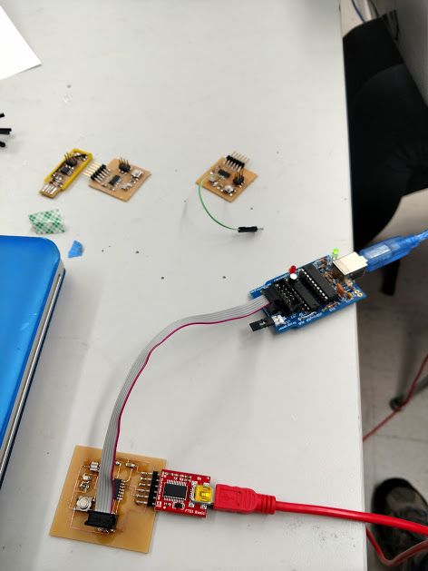
All connected up. Green LED is a good sign!!
I then went back to the terminal/command prompt and typed "make programusb-tiny". NO errors! I then flashed the fuses using the similar command "make program-usbtiny-fuses". The red LED flashed while the programs were being sent to to my PCB.
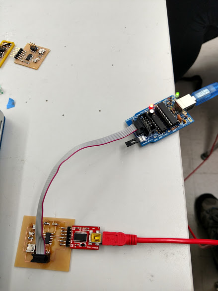
The red LED is on while the programs are being sent to the PCB
FINALLY, I had to test if the programs did what they were supposed to do. I opened up the Arduino program to take advantage of its easy to use serial monitor and chose the FTDI as the serial port for Arduino to interface with. I set the baud rate to 115,200 so it would know the speed. I typed some letters and they echoed back to me on the serial monitor. It worked!!!
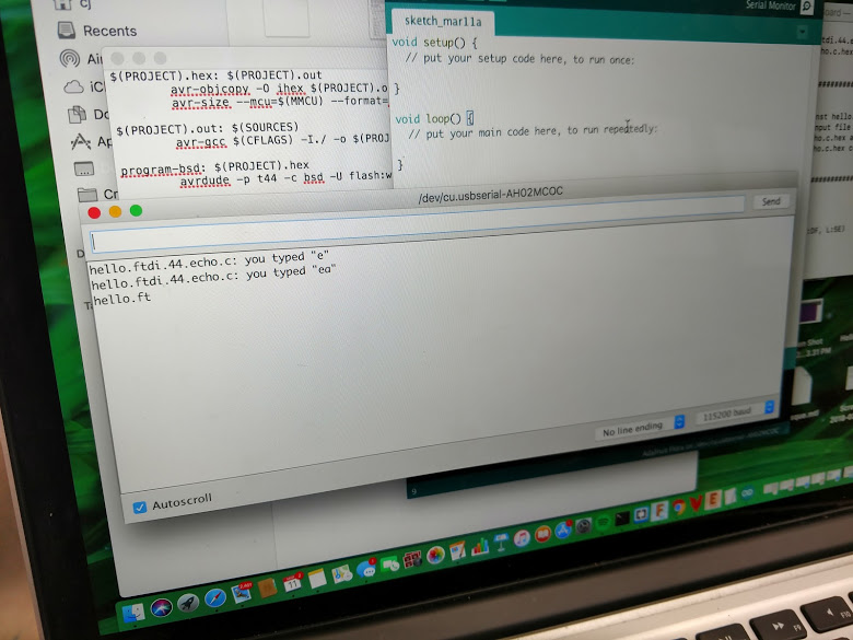
Hello World Board echoing back my typing!!!
Overall, this has been the hardest week so far in terms of learning new things and having to repeat myself, correct mistakes and really stretch myself. If it weren't for the help of Adam Harris, FabLab 2014 I'm not sure I would have ever really figured out or understood the programming aspect of the assignment, but now I feel like I at least partially get it and with a lot more thinking and reading I hope to be able to fully understand it on a deeper, conceptual level for the next electronics assignment.