01
03
09
10
If it smells like chicken, you're holding it wrong.
11
The assignment for this week was to make a own design for the hello.ftdi board. This was the second time for me, designing a PCB. :)
12
As I have done a long manual for using KiCad in week 4 additional to the normal assignment, which was only producing a PCB, this assignment will be a bit shorter.
KiCAD Tutorial:
Stage 1: Schematic, create parts/footprints, routing
Stage 2: PCB production, milling
Stage 3: Soldering, initial startup
13
Neil gave us the task to add at least one LED and one button. I thought about this and added 3 LEDs and 2 Buttons. One (the green) LED is a simple "hey-dude-their-is-some-current" LED which is simply connected between +5V and ground. The other two LEDs change while sending data from your serial terminal to the PCB. Every time you send a letter, one LED turns of and the other turns on. It's a simple way to give a optical feedback to show that there is communication between the helloFab and the FTDI cable.
To get this option, there are only some lines code needed. Here are my project files and firmware...
14
Download my helloFab KiCad project (open with Nightly Builds after Sept'16)
16
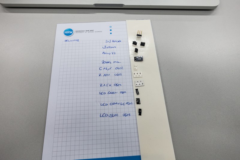
First of all, the BOM:
1 ATTiny84-20SSU 68T3784 Newark
1 FQ5032B CRYSTAL, 20MHZ 61T5356 Newark
2 MC32882 switch 67P3661 Newark
3 LEDs 0603 (in stock before)
1 1µF 0603 capacitor (in stock before)
2 18pF 0402 capacitor (in stock before)
3 1.5k 0603 resistor (in stock before)
3 10k 0603 resistor (in stock before)
1 1x6 pin header (in stock before)
1 2x3 pin header (in stock before)
17
To gain the knowledge, how to connect all the parts together, the best way is to use the, by the manufacturers supplied datasheets.
The schematic shows the ATTiny, the switches, all 3 LEDs, the FTDI header, the ISP header and the crystal.
It is divided in 5 areas:
The upper left area shows the ATTiny, the LEDs and the switches with their pull-down resistors.
The upper right area shows the FTDI header, which is used to communicate to the computer and is directly connected with ATTiny and supplies power, if used.
The lower left area shows the ISP header, which is directly connected to the ATTiny to program it and supplies power, if used.
The lower middle area shows the power on LED.
The lower right area shows the crystal and the needed capacitors.
18

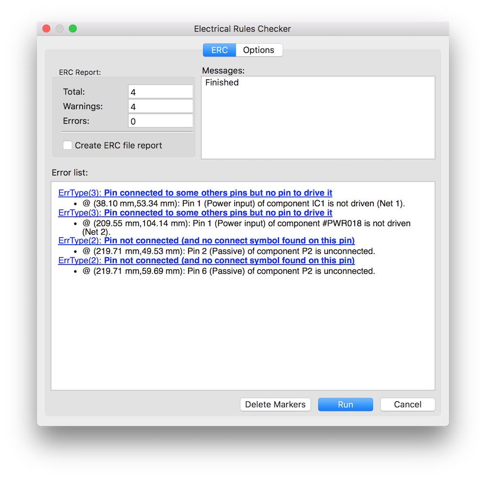
After drawing the schematic, the ERC was obligatory. It returned no errors. :) The warnings are ok - they just say: "something is not connect, please check this". As my PCB is powered external without any onboard power distribution, ignore the warnings.
19
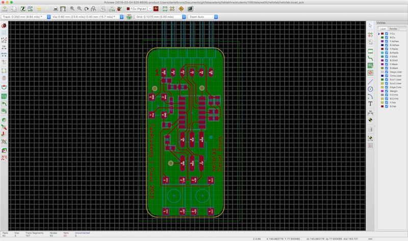
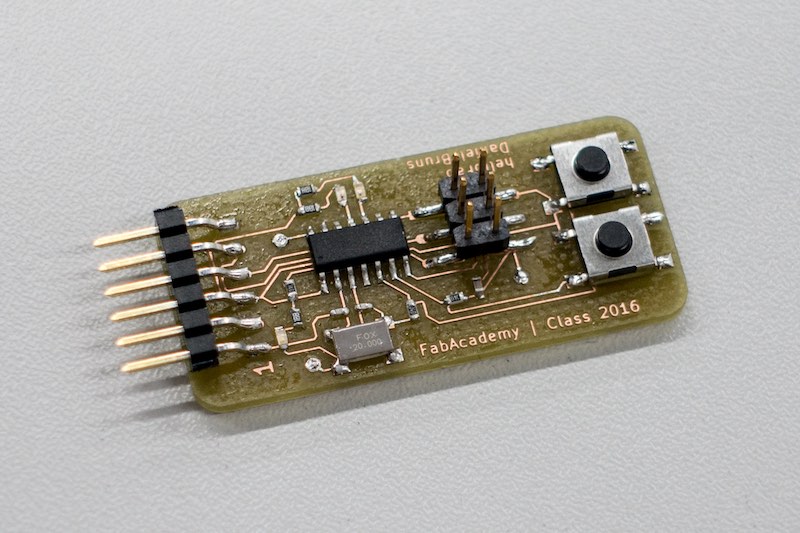
This is my finished PCB. The ATTiny is nearly in the middle of the PCB, above, there is the FTDI header, below the ISP header. The crystal is as near as possible to the ATTiny. The switches were placed below the ISP header.
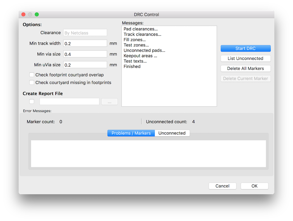
The PCB was milled on our LPKF S63 and soldered by hand.
It's DRC time! No errors! As mentioned before - after checking the warnings, they can be ignored.
21
If you ever had problems sorting your parts while soldering, just use some double-sided tape.
23
This is my finished PCB after soldering by hand. Not the prettiest, but it worked. :)
25
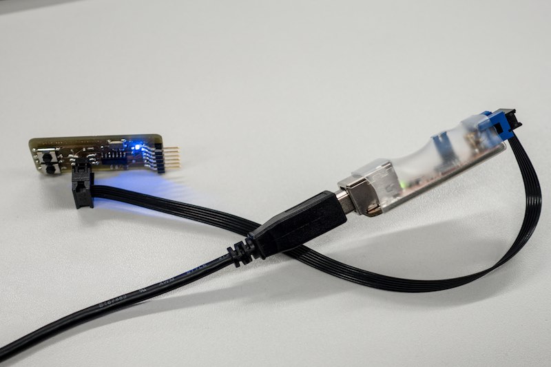
The helloFab PCB while programming with my own FabISP with the firmware, as done in Stage 3: Soldering, initial startup :)

This work by Daniel Bruns is licensed under a Creative Commons Attribution-NonCommercial-ShareAlike 4.0 International License.