final project -- about me -- weekly assignments -- fab academy
Real Transistors... And Planning
Real Life has reared its ugly head again, and I'm spending more time working on work-work than I had hoped for. Which, of course, mounts delays upon delays here. So, this update is more than a month late, and it doesn't do everything I wanted to have done six weeks ago. Plans will have to change, expectations to be lowered...
The PCBs arrived
The PCBs took around two weeks to arrive this time, so it wasn't really a long wait for them. I also ordered stencils for applying solder paste, to save on (a lot of) work when stuffing them.
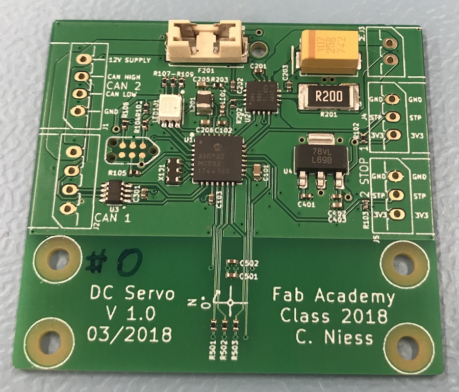
Build-A-Bear Board
I didn't take that many photos when stuffing the boards, mostly because it was quite late at night and I was too busy doing it. The process is not exactly new, though, and I have a good set of photos to do a separate documentation page on it.
Motorboards
So, for now, results. First, one of the motorboards with solder paste, but before I put on the components:
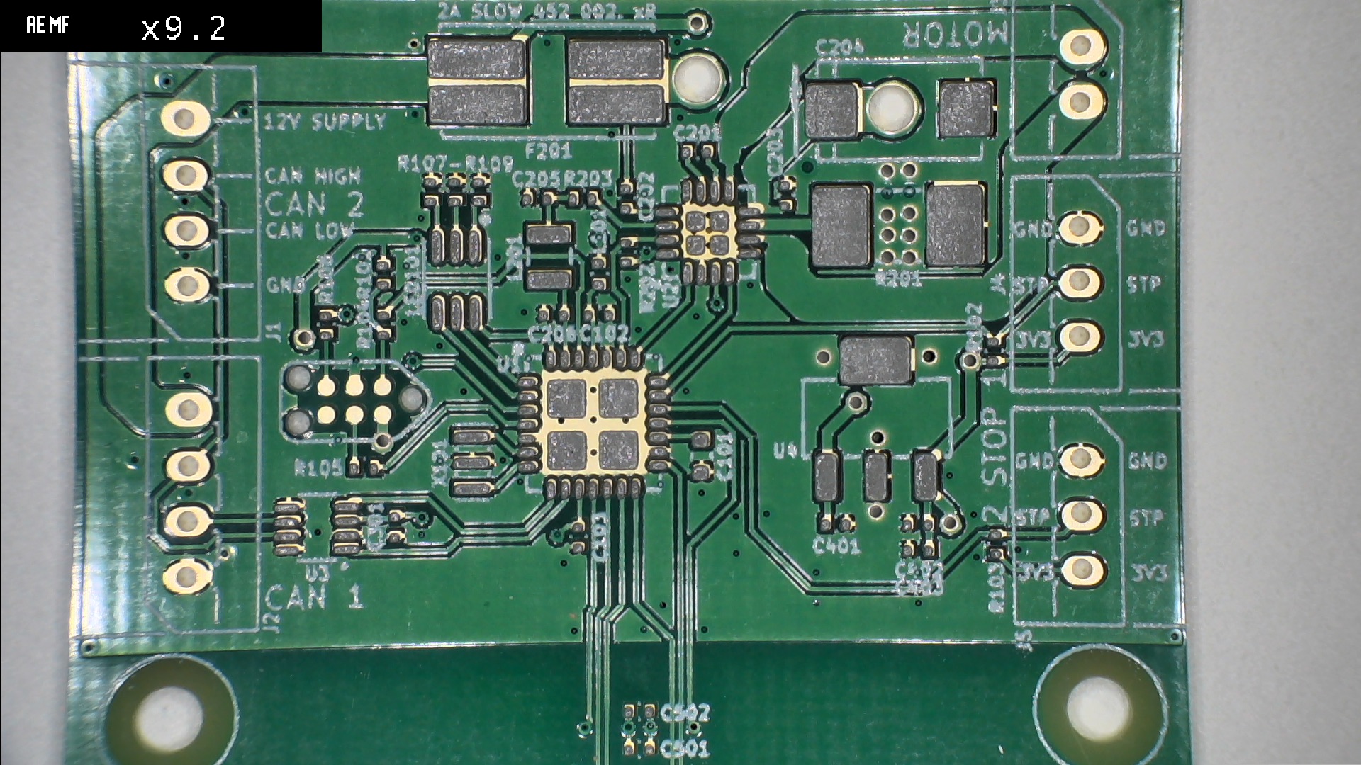
The solder paste was applied with a stencil, which is generally preferable to most kinds of manual applications. It requires making a stencil, though, which is a step I have yet to try doing at the lab (it should be possible to use a laser-cut thin plastic sheet).
The slight offset visible mostly around U3 at the bottom left is not critical and can be ignores as long as it's not too big. Molten tin has an incredible amount of surface tension (as in: It wants to become a compact little ball by all means), so it is strong enough not only to pull that solder paste blob onto the pad, but also to pull most kinds of components into a well-centred position on their pads. It's pretty impressive to see when that happens, I'll have to make a video of it at some point.
After about three minutes at 265°C in the trusty drying / general purpose oven of the chemistry lab, the boards come out looking nice and soldered with all SMD parts on them:
With a stencil for putting on the right amount of solder paste in the right places, the amount of corrective work is generally low. The stencils were not purrfect, of course - The openings should be just a little bit smaller than the pads, by an amount that is usually determined by testing, or just guessed. I forgot to set any kind of size reduction, so I ended up with way too much solder paste on the pads. Which is not a huge problem for resistors, capacitors and components like them - Those will just have a bigger solder fillet, and be mostly OK. It can be a problem for QFN, though, and any kind of fine pitch case. The microcontroller on the brain board is a fine example of that. Or the CAN driver (U3 on the motorboard), so I had to do some rework there on some of the boards...
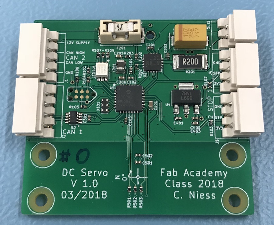
As a next step, I soldered in the jacks for power/CAN, endstops and the motor:
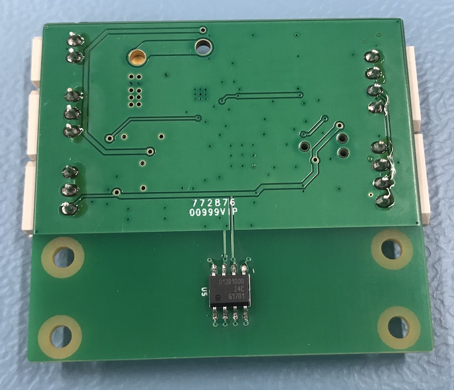
Then, I flipped the boards, and put on the magnetic angle sensor. It would have been possible, in theory, to solder that one on in the oven, but I for a single component like that it was just way too much work to do so (and have to live with having something fragile hanging from the bottom of the boards while populating the top).
Braaiiiinzzz
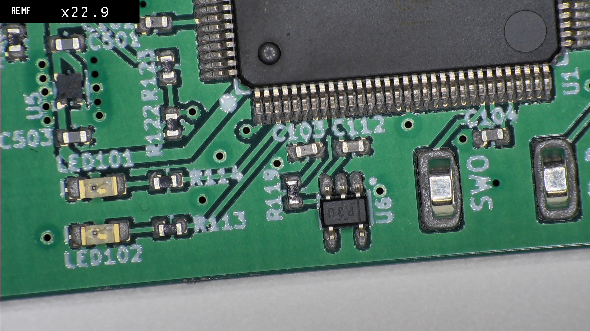
Next, I did the brain boards. They are quite simple boards, so they didn't take nearly as long to stuff as the motorboards did. They require a lot more rework, though.
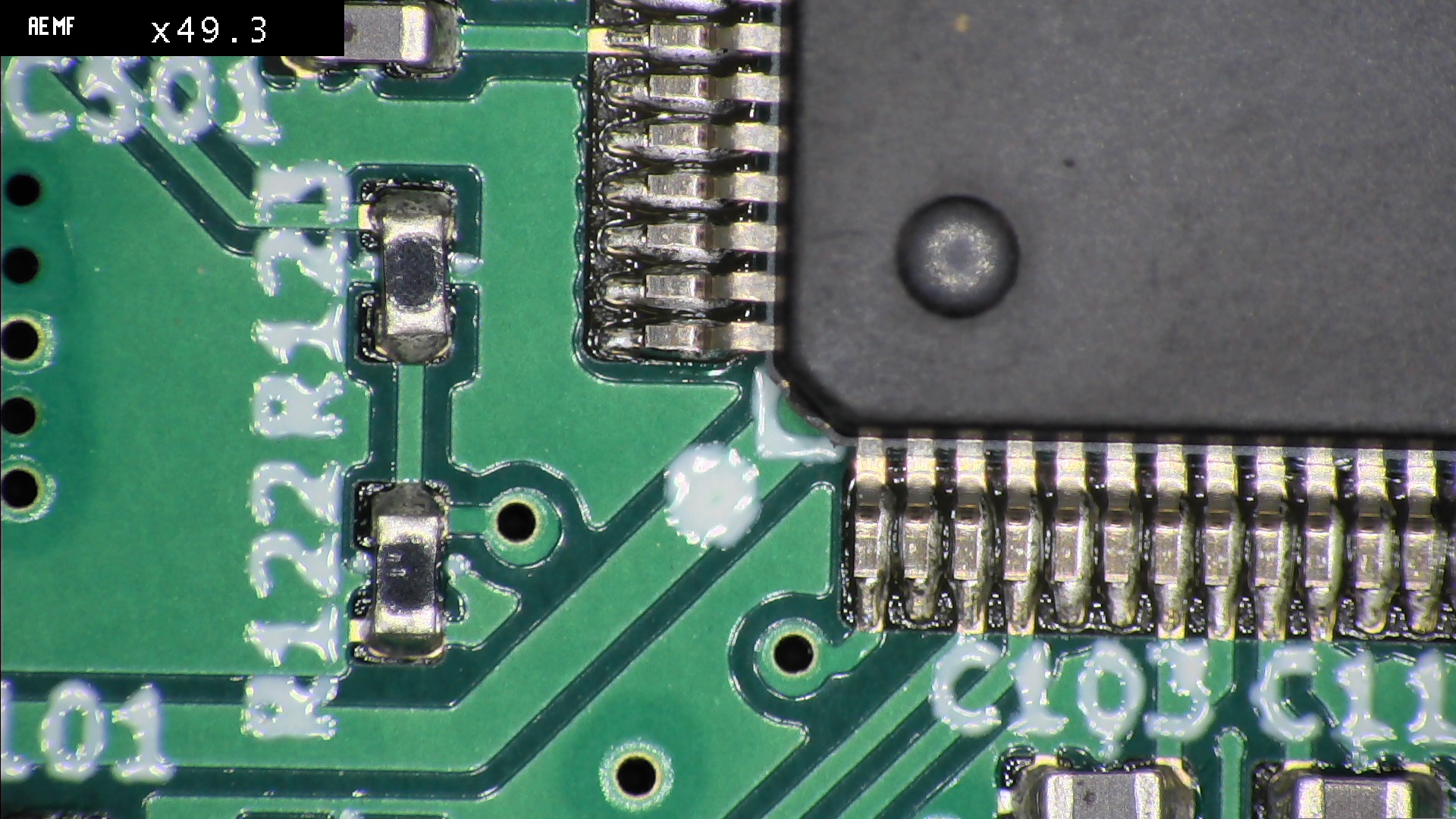
Starting out, the boards were treated the same as the motorboards: Paste applied with a stencil, components put on with tweezers. I took a detail shot of the microcontroller at that point:
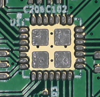
Again, there is a lot too much solderpaste on those pads, so it bulges out a little more than usual. The QFP case of the microcontroller with its long, close together pins is really prone to tin bridging, so it was a bit of luck that, with too much solder paste, I still got one that had no bridges:
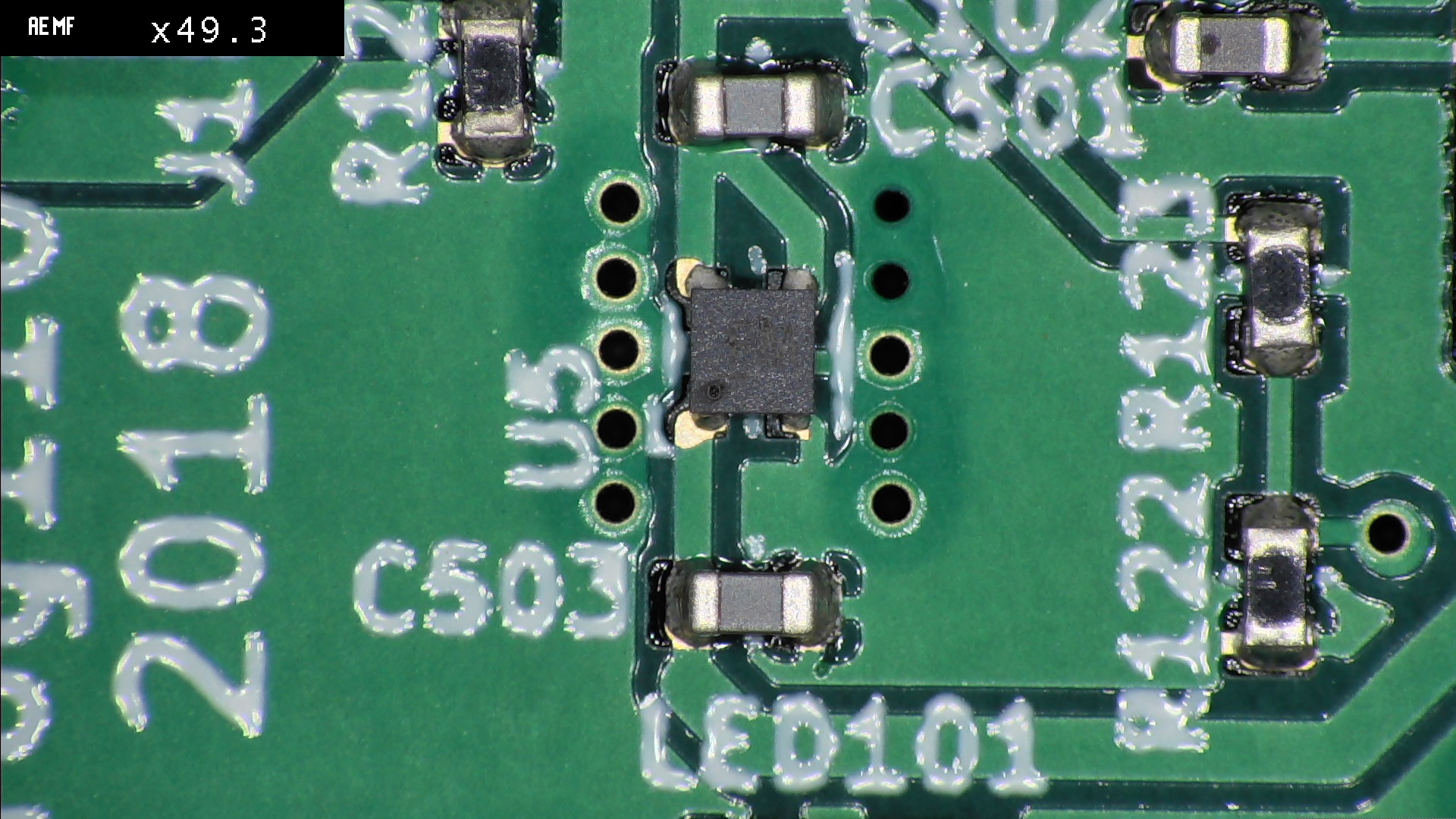
Also, that little nub on the left of the first picture, U5, was an experiment I first did some weeks ago. It's a small voltage regulator, a square case of 1x1mm, with 5 pads underneath. It mostly fits into the usual design rules of chinese prototype fabs (excluding the thermal VIA in the center pad that might help under high loads), but barely. It seems to work, though, as this is the fifth one I used, and all of them work:
Oddities
After quite a few years of building my own electronics, I'm still learning something new every time I dive into the lab. One nice (and, luckily, noncritical) oddity popped up with the motor boards:
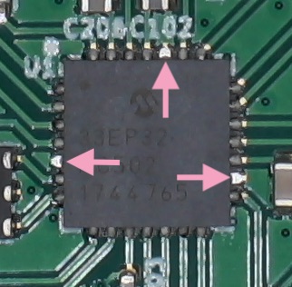
With all the motorboards I made, those three "pins" of the PIC were left with way less tin than the others. It's not critical, there is a solid soldered connection between the contacts of the QFN and the pads of the PCB. But it looks strange, so I had to find out why it happened.
The reason, as it turned out, was quite simple, and stupid. I had tried to actually match the design rules of the fab I ordered the boards at, specifically their rule on the minimum width of soldermask slivers. I had not done that before when ordering there, and they had flawlessly made boards with a lot slimmer soldermask details without as much as a complaint, but with those boards, I had the mad idea to actually humour them. This resulted in one detail of those boards being omitted:
Usually, there would be a "dam" of soldermask around the centre pad, covering the tracks connecting the ground pads to the center pad and keeping tin from netting (and flowing into) that area. Those dams were too thin for the design rules the fab officially has, so the tin of those pads partly vanished towards the centre pad...
Plans, Deadlines and Mechanics
I was mostly blocked from doing anything to my fabacademy stuff for six weeks, and will only have a limited amount of time over the next few weeks, so my plans will have to change. First of all, This final project gets the highest priority now, given that the presentation date is on fast approach. Second, I will have to lower my expectations of what I want to show in that presentation... By a lot, if necessary.
What I still want to achieve is a mechanically sound device that can lift components and put them onto a PCB. It has to be electrically driven, but I will probably have a very, very simple input device for that in the first version, with very unfancy control of the motors. That is enough to actually use the placer, albeit not the convenient tool I want to have in the end. I can't bend time, though...
final project -- about me -- weekly assignments -- fab academy
