Electronics Design
March 4, 2015
Assignment:
Redraw and make the Echo Hello-World Board.
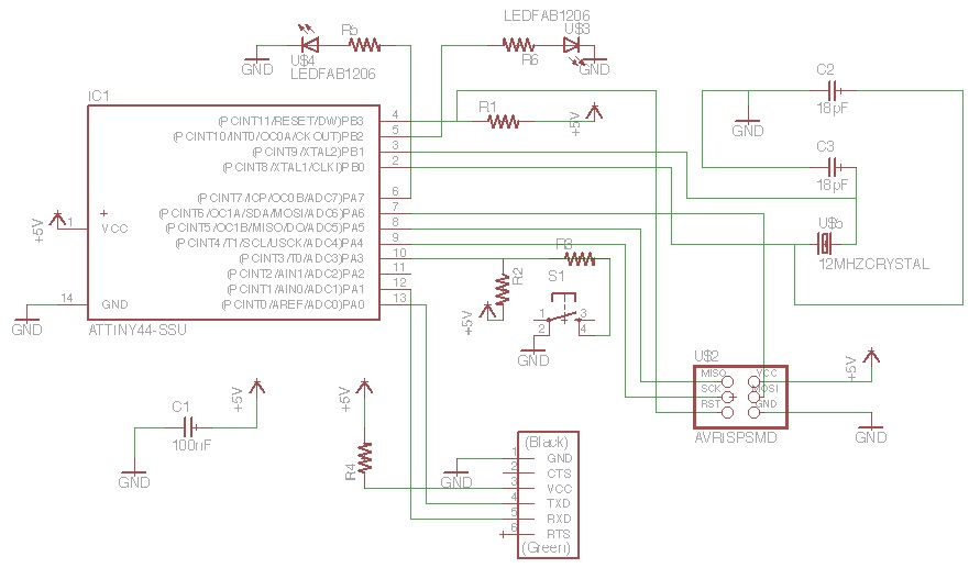
The first step was to download Eagle as the tool to design the Echo Hello-World PCB. I then downloaded the fab.lbr library file from FabAcademy into my new project file. After which, I began to "add" all the necessary component parts into the schematic design. We are to add LED lights ( I chose to add two) and a button to the already designed Echo Hello-World Board:
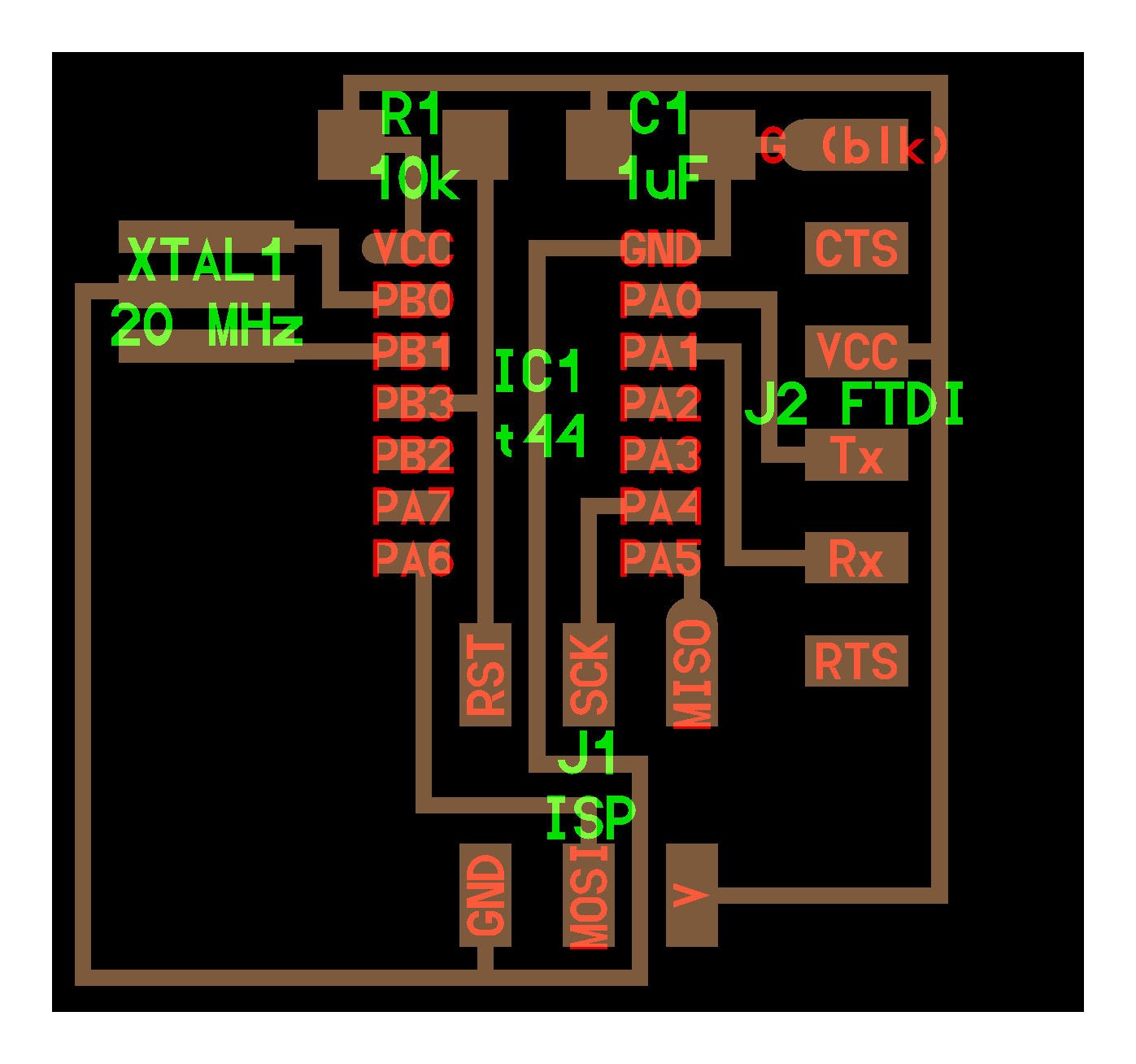 The six pre-determined component parts from the Echo Hello-World Board are:
IC1-t44: An Integrated Circuit AT-Tiny 44-SSU AVR Microcontroller
C1: An unpolarized 1uf Capacitor, imperial code size #1206
R1: A 10k Resistor, imperial size #1206
XTAL1: A 20MHz Resonator with built-in capacitors.
J1 ISP: An In-System Programming Jumper, AVR 2X03 SMD
J2 FTDI: A jumper between the PCB and the USB in computer (FTDI is a company brand name).
The 20MHz Resonator replacement:
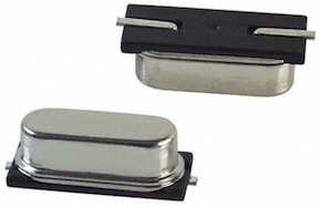
As we didn't have the 20MHz Resonator required we replaced it with a 12 MHz Crystal Oscilator and additional two 18pf 50v external capacitors. This particular Crystal Oscillator wasn't in the fab.lbr library, so we proceeded to download the data sheet for our Crystal Oscillator: CSM-7 SMD Quartz Crystal. In the control panel of Eagle I "right-clicked" to create a new library within my "Hello World Board" Project which I named: "Hello World.lbr" Double click to open the library. Then, to create a new device: click on "devices" and write a "new" name for your device. Then, under "package" you can draw your new device or select an existing device which you could then modify. We were able to modify an existing crystal from the fab.lbr library into our in-stock crystal component changing its dimensions. When we finished modifying the package we renamed it to our new device name. Then we added a symbol "add" which we chose from the preexisting fab-library and renamed with our new name. Lastly, we connected the package to the symbol "connect". Here, you can rename the ports to where they should connect.
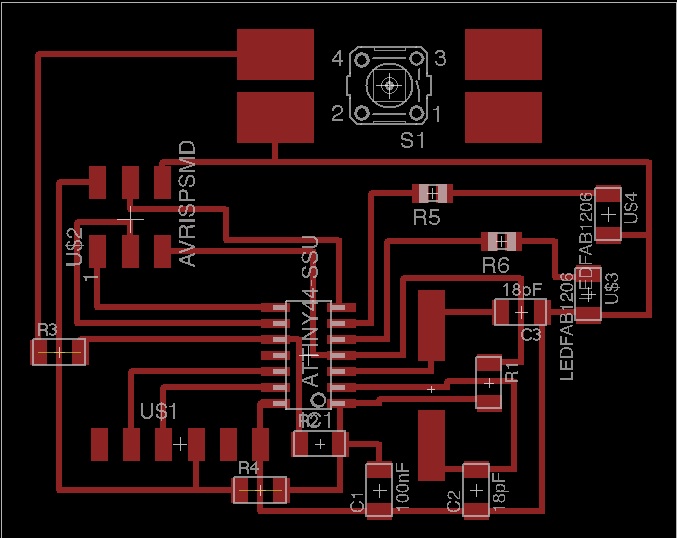
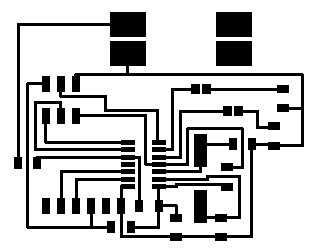
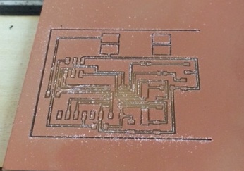
In the Schematic mode I "wired" all necessary components as follows: After determining how to achieve the best possible layout, I came up with the following design: I used the same parameter values as with the FabISP PCB milled on the Electronics Production week. To my surprise, some tweaking was needed as the Zvalue was too deep and the end mill broke off. At the end, the board was milled successfully but with a three sided edge to it. This edge came from the border of the png file, but since it was outside the board itself, it didn't really matter. Then, I changed the milling bit to "cut" the border of the PCB. Unfortunately, the border was off-centered from the board, cutting into the board, hence ruining the board... Since I had no experience with etching a PCB, I decided to try to learn another technique for making PCBs, etching.
Adding a new device into your project library:
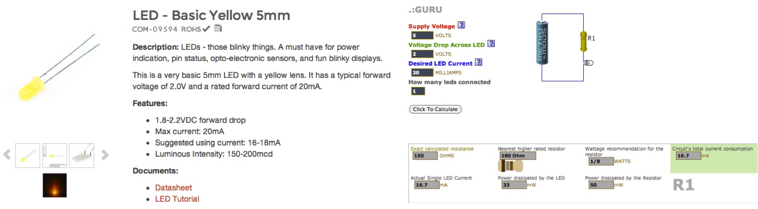
We also added two LED lights together with their required resistors. To calculate the resistors required we used the specifications from the data sheet of our LED lights in stock and calculated using an online LED Light Resistor Calculator. As we don't have a surface mounted LED device we adjusted the hole through LED into the surface mounted LED device's pads.
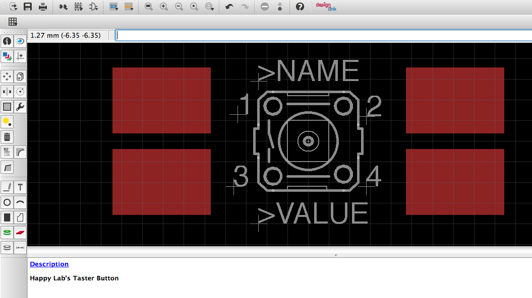
Another component to add was our switch, since our switch looked similar to the Omron Switch in the Fab.lbr library but with different dimensions, I proceeded to modify the Omron Switch file saving it as a new component. I then added it to my library and renamed as "Happy Lab's Taster Button." 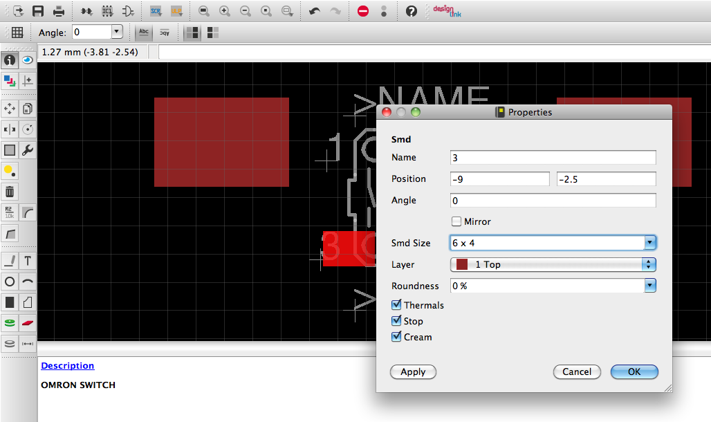
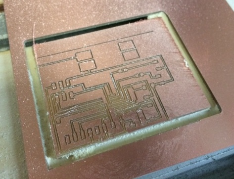
Milling the PCB:
Etching the PCB:
I printed my circuit board in black ink mirror imaged on an overhead transparent film. This will act as a mask, when exposing the board to UV light. Then, I peeled the blue film off the Photoresistant PCB blank board, which I had cut to my required size. I then exposed the photo resistor side of the PCB and the circuit printed on the transparency to UVlight for 2:20 minutes. In the meantime, I mixed 2grams of PCB developer with 150ml of hot water. I then dipped the exposed photo resistant board in the developer to remove the photo resistant layer off from the board but not from the traces. You have to be careful not to over develop, since this might eat away the circuit traces as well. I proceeded to rinse the board with water. Afterwards, I submerged the board in the chemical Natrium Persulfate at 50 degrees Celsius for approximately 30 minutes. When heated, this chemical produces bubbles which in turn "agitates" the solution helping dissolve the UV exposed copper.
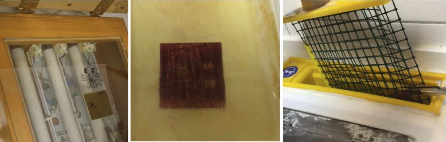 After 30 minutes, with constant checks, portions of my board had dissolved, while other portions not, so I decided to leave it in the chemical for a longer time. Unfortunately, this resulted in dissolving some of the copper from the traces as well. This proved that this chemical etching process is a fine balance between chemical exposure and time. Consequently, I proceeded to re-do the above steps once again.
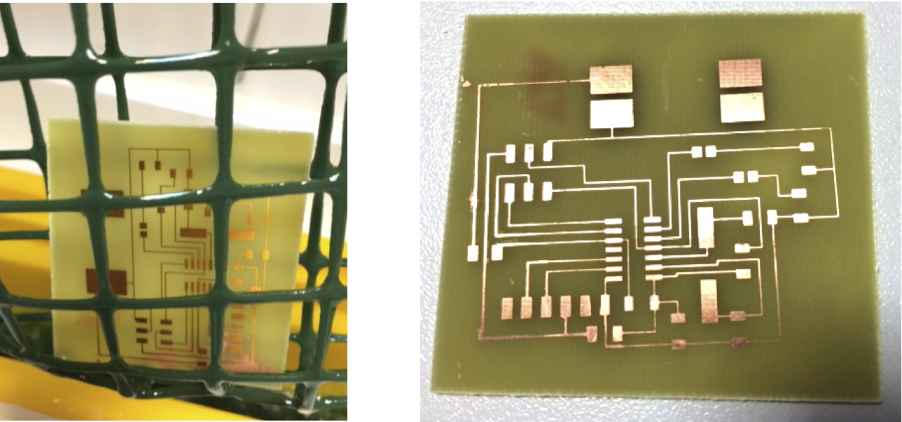 The second time around, I carefully monitored the traces and got it out from the chemical right on time. I then proceeded to expose the board once again to UV light for 2:20 minutes in order to remove the photo resistor from the circuit traces. And once again submerged the board in the photo resistor developer solution. This is necessary in order to expose the copper and be able to have a good contact to the copper when soldering the components.
Here are the links to my Electronic Design PCB Files:
Electronic Design PCB G-Code for Milling
Electronic Design Outline PCB G-Code for Milling
Electronic Design PCB Etching Mask
Final PCB:
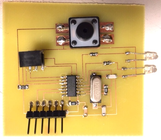 The result was very good, so I proceeded to solder all components according to my design.
