
Electronics Production
February 18, 2015
Assignment:
Make the FabISP in-circuit programmer.
The FabISP is an in-system programmer for AVR microcontrollers, designed for production within a FabLab. That is, it allows you to program the microcontrollers on other boards you make, using nothing but a USB cable and 6-pin IDC to 6-pin IDC cable.
Making the PCB Board:
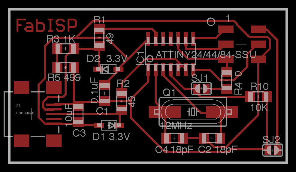
I decided to replicate the FabISP designed by David A. Mellis and proceeded to download his FabISP.png files for the circuit and contour.
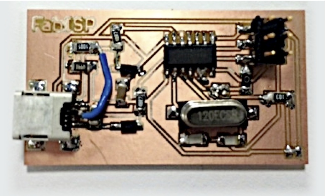
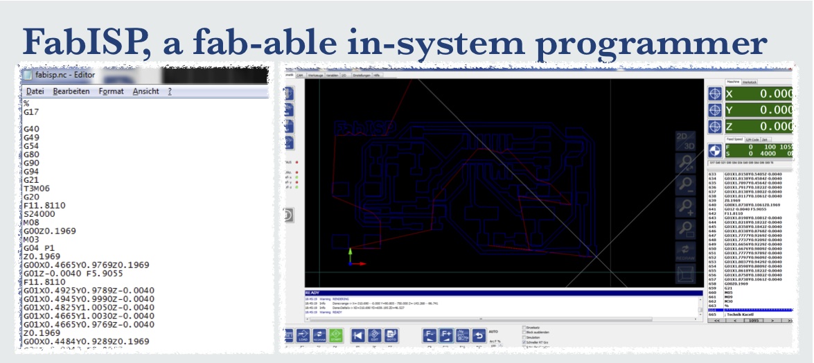
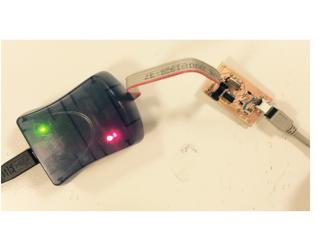
Using MIT's FabModules we generated two numerically controlled set of instructions in order to build the circuit board using a computerized machine tool, the CNC Mill. The set of instructions were generated in a G-Code. Basically, it is a series of coordinate commands that define where, how fast and through what path the CNC Mill moves in order to be able to mill the PCB (Printed Circuit Board). These are the adjusted parameters for our specific HappyLab CNC Mill: This was definitely a learning experience as it was not only my very first time soldering but also because the components were SMD, surface mounted devices. I began by practicing soldering before soldering on the final PCB. I did the smallest components first and soldered in a clockwise path leaving the USB connector for last. Well, I was shocked to see how narrow the 5 traces were and found it almost impossible to have a good solder without making a bridge. I needed to de-solder the USB connector, which proved to be very difficult and when lifting the USB connector from the PCB, copper came off with it, ruining the PCB. This resulted in milling a second PCB. The second time around I made sure to start with the USB connector, unfortunately I soldered it too inwards which proved difficult to solder the fourth trace. Determined not to mill yet another PCB, the solution was to use a jump wire. Hence the beautiful blue wire on my PCB. After checking the PCB with a multimeter and making necessary corrections we continued with downloading the AtmelStudio software (in accordance to the brand of the microcontroller used in the PCB) in order to program the FabISP. When connecting the power to the FabISP, it showed that it was withdrawing too much power, an indication of a short circuit. We then identified the problem, de-soldered it and continued with the programming which was then successful.
Here are the links to David A. Mellis' FabISP PCB Files:
We then modified the units of these two G-Code files, the one for the etching of the circuit and the second for cutting the contour from inches to mm. Two different G-Codes were used in order to take into account that we were using two different mill bits, a 3mm Diamond Head Bit for cutting and a 0.4mm End Mill Bit for etching the circuit. The mentioned drill bits were decided together with the lab manager and fellow student, after a few trials and errors, determining them to be the best option for the job. The End Mill Bit has a constant width making it the best for the etching. The other modification to the G-Codes were the thickness of the lines to work best with our drill bits.
These are the new G-Codes:
Circuit Board Milling 
Circuit Board Contour
Output:
Cut: 5
Plunge: 2.5
Job Speed: 75
Job Height: 5
Spindle Speed: 24,000
Tool: 1
Coolant: 1
Process:
Cut Depth: 3,175
Stock Thick: 0.1
Tool Diameter: 0.4mm 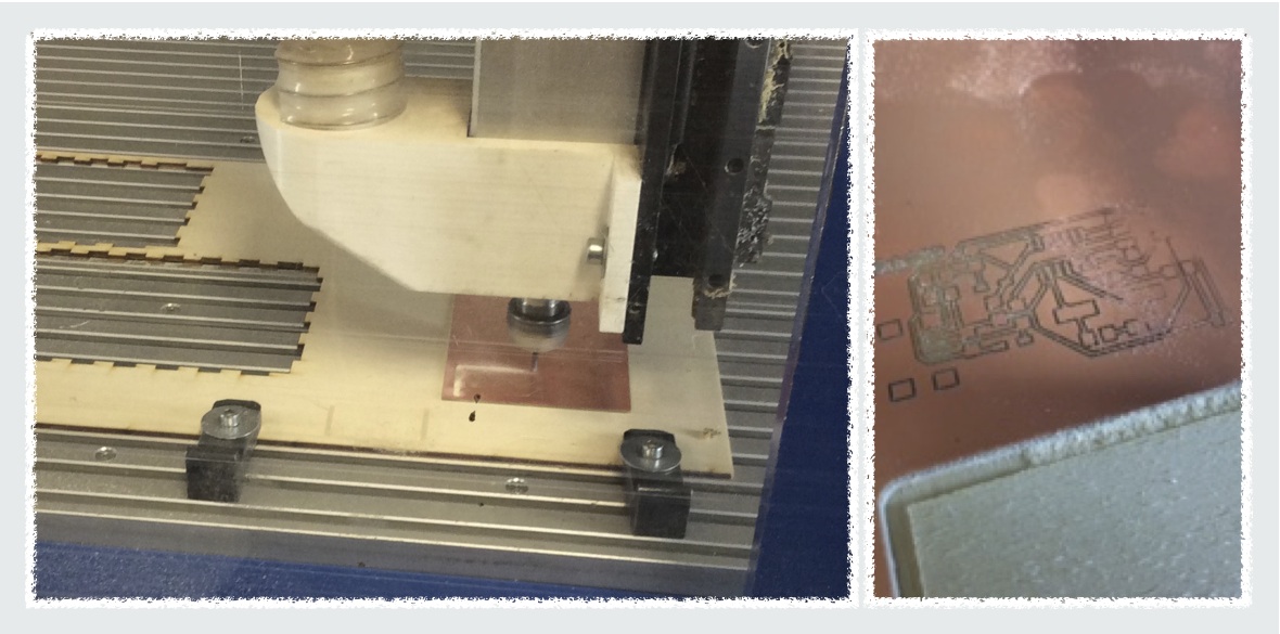
Soldering the Printed Circuit Board:
Soldering Layout:
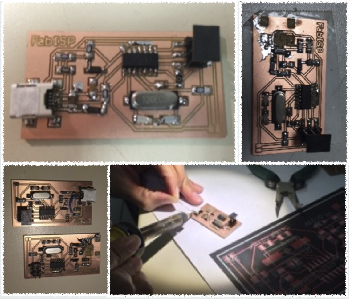
My final PCB,
the FabISP In-Circuit Programmer
Programming the Printed Circuit Board:
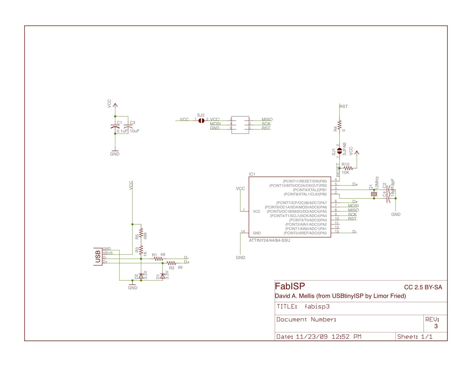
FabISP PCB Schedule Design
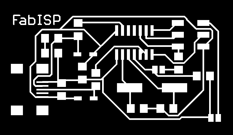
FabISP Devices PCB Board Design
FabISP PCB Etching Mask
