Electronics Design Class
6th Worldwide gathering for Fab Academy 2015 feat. prof. Neil Gershenfeld
18 February
12 weeks to Final project
ELECTRONICS WORLD, a brief Intro
The Components [+]
- wire
- button
- resistor: I=V/R
- capacitor: C = Q/V, I = C dV/dt
- unpolarized
- polarized
- crystal, resonator
- inductor: V = L dI/dt
- diode: current from anode to cathode
- PN
- Schottky
- Zener
- LED
- transistor
- bipolar: collector, emitter, base current gain
- mosfet: source, drain, gate resistance
- battery, regulator
- op-amp: differential gain, negative feedback
- microcontroller
- sensors
- actuators
The Current [+]
- power: P = I^2 R = I V
- EDA
- hierarchical, parametric drawing
- packages, footprints, component libraries
- design rules
- schematic entry, component placement, routing, simulation, fabrication
- drafting tape

Used components (from top to bottom, left to right):ISP, FTDI, 20mhz resonator, Red LED, Green LED, attiny44 microcontroller, button, 10k resistor, 1uf capacitor, pull-up resistor, milled board, ribbon wire
The theory, basic dynamics of electronics
So first of all not knowing previously the world of electronics was a bit of a set back. Or better said, it demanded time dedicated to lerning the basics.
On my researches found:
- Basic Electronics learning Tutorial on Instructables website.
- Video on OHM's Law
Also ended up at Ladyada.net where you can find a lot of very detailed and informative notes on all sorts of electronic practical and theorectical subjects.
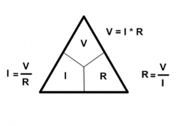
OHM's Law. Relation between Voltage, Intensity and Resistance.
Echo hello-world board The Recipe
So for the redesign of the bord it was recommended that a replica of the design given by Professor Niel was done, so that we could start understanding the hierarchical relation between components and how, indeed, the board can be assembled in a orderly fashion and current can flow flawlessly with minimum setbacks.
If you are using Eagle for the first time, before going crazy looking for the right components add the very handy fablibrary where all the components used during the curse are organized and correctely represented with an up-to-date graphical representation.
Eagle is a very organized step by step software that allows you to plan the layout of your PCB. If this is your first try, as it was for me, you may find the representation of the schematics a bit akward and if you are a more visual person, as i am, you may get a better idea of how everything works once you move to the layout of the actual board. Once there replacing and shifting components to improve design is quite easy. At this moment you should have your components named and with an added value, and air wires should have been replaced by non-crossing traces. Check all conections twice, trying in advance to build the shortest path for the traces between components reducing as much as possible the probable soldering overlapping if everything is underdimentioned.
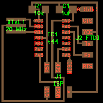
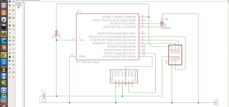
Prof. Niel Design for the echo hello world FTDI 44
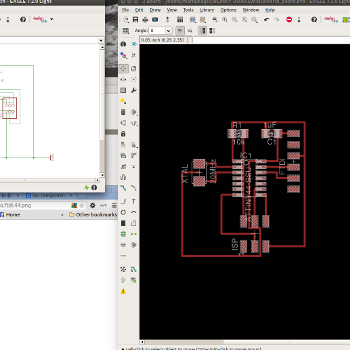
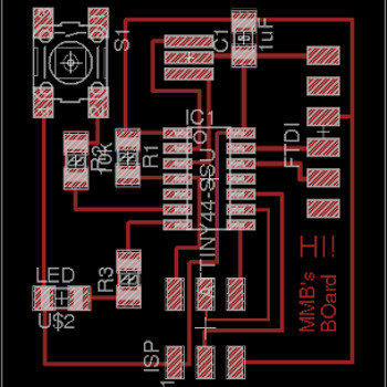
my own version of the hello world FTDI 44 redesigned in Eagle
Software used:
- on board design and schematics
- Eagle 7.2.0
- Kokopelli [RETRO]
- on board customized image and cut lines
- Gimp
- on board programming
- Assembly
- Arduino 1.6.0
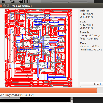
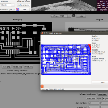
From the exported image I went to Gimp to generate its outline and and ajust text weight. Next was milling the traces with the Roland modela via Fabmodules which is quite straight forward process. Having done this before you just have to be sure you place the .png's origin in a free area with good enough margin to fit the hole PCB and its cutline
Also correctely placing the 1/64 bit (for traces) and 1/32bit (for cut) is key to get a good final result
My final milled PCB board wasn't perfect, but it was ok. Trace lines came out a bit thin because i went a bit over the amount of offset I should have set. But still good enough traces, suficient copper surface.


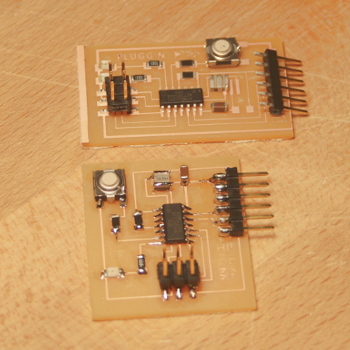
Still willing to improve and mill a bit more went back to eagle redrew it to diferent proportion PCB, making it a bit more wider and less taller shifting the FTDI to one extreme for practical physical connection
The only problem when you are focoused on form and proportion is that you miss a few practical mistakes that should have been detected before moving to diferent design or milling for the second time.
Well, learning from mistakes!
More than cool-looking, the new milled board was as defected as the first one and so I had to just get back to the first milled stuffed board to check connections and debugg.
Didn't get to solder the second board because it was, indeed, useless.
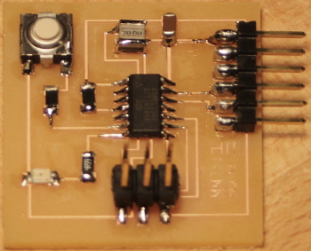
Milled and stuffed board, had miss placed conections, after debbuging was OK (see picture below)
Failiures:
- With Francisco and a multimeter we figured out the crucial mistakes I did like missing a connection from ISP MOSI - Master Out Slave In, a signal on the Serial Peripheral Interface Bus - to correspondent Pin PortA 6 because you are playing arround the layout design is pure newbie stuff.
- The same goes for the buttons missing external pull up resistor and missed connection to the Vcc Power supply. After some dissoldering I hadded a 0 OHM resistor for "bridging" and switched position of the resistor so that it could conect to the nearest Vcc


Improvements - Fixing the Hello World board
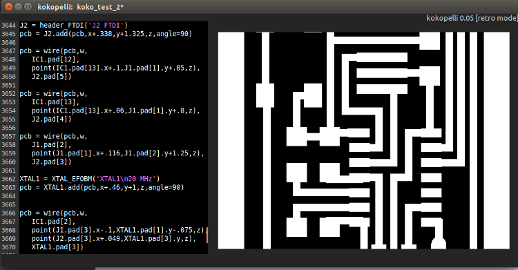
Because energy was still high we went for a deeper experience in coding, building traces in Kokopelli latest version [RETRO] for a more compact design of the Hello World Board.
Conections to the 6 pin connector were redesigned and traces where done thicker and two leds instead of one were added
That was this weeks work. Have to say I've enjoyed the trip into electronics world!