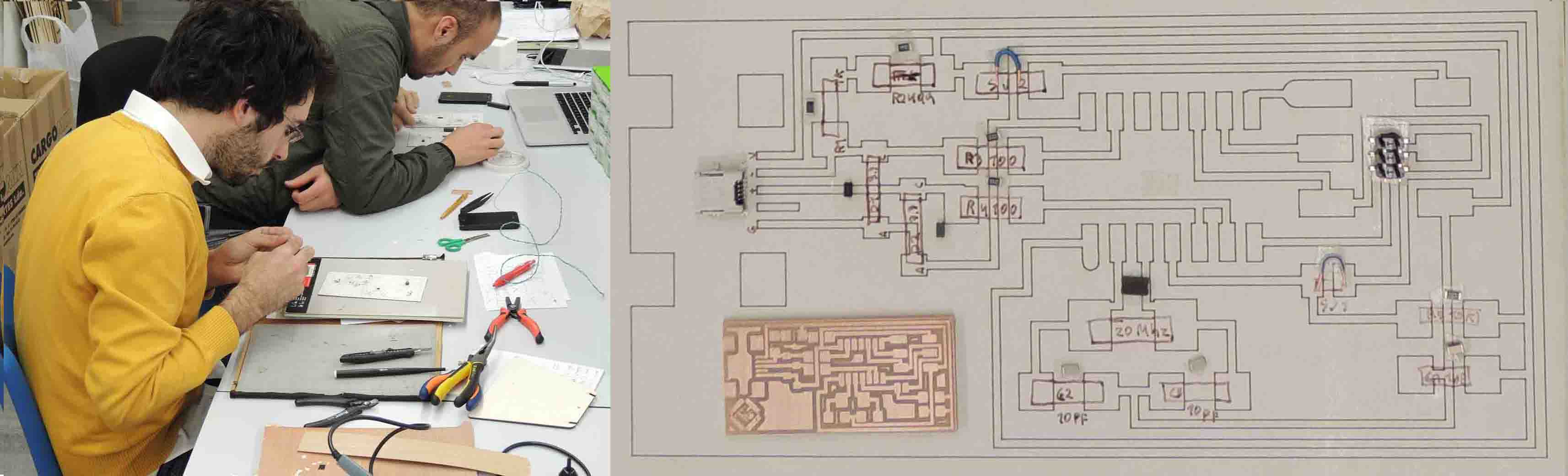
Flat means Flat
Everything needs to be flat, flat PCB, flat modela plate, flat sacrificial plate.
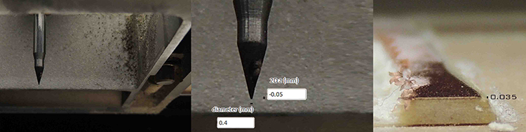
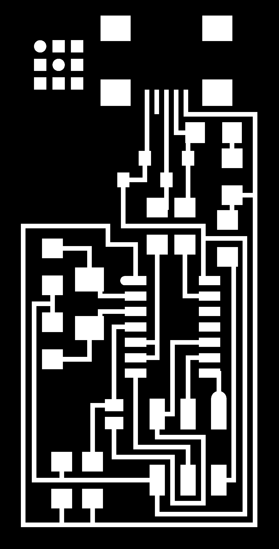
When everything is set (collet + 1/64 mill, plate + double-sided tape + MDF sacrificial board + double-sided tape + PCB), I nedeed to find the origin (left inferior corner), move the x(min) and y(min), then move the tool down util it just touch the copper, then we sent the interior trace just to evaluate the copper flatness, deppending on that we set the 2D z upper or lower to mill the copper.
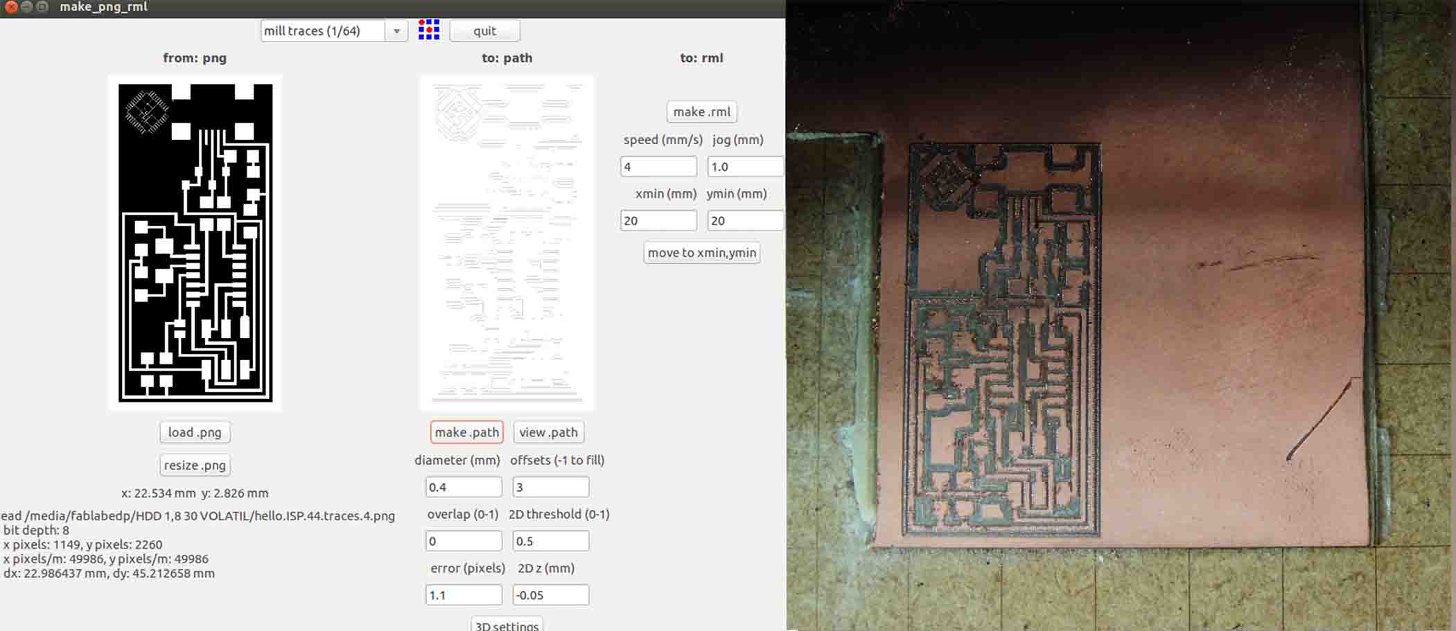
Now it's time to mill the traces, it's everithyng set up unless the traces png and the settings. For the 2D z, we used "0.5mm" to mill all the traces.
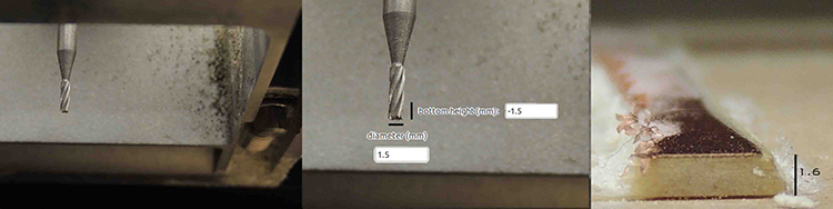
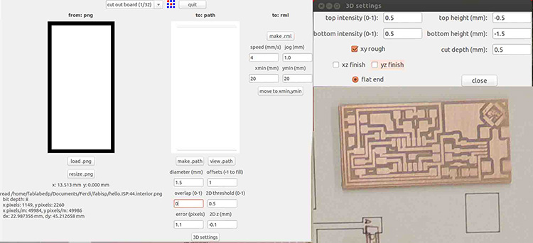
To cut the interior, we used a 1.5mm diameter tool, set the interior png
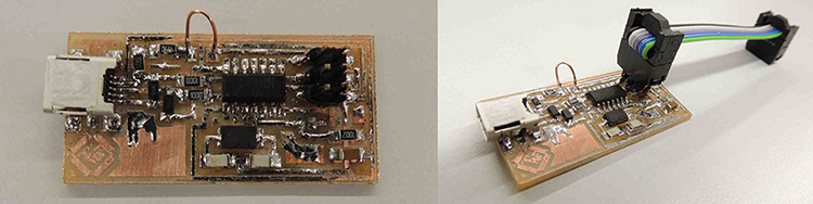
Stuffing
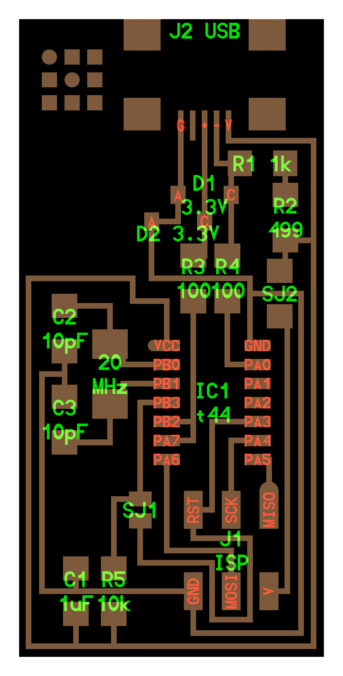
To stuff the board we made a big template of the ISP, then carefully place every component correctly oriented, hello.isp.44.png was a big help.
Soldering was a BIG mess, i've never soldered such a tiny components, next time i will listen to Neil method (apply little bit of solder in the pad, then place the component, reflow the pad and the component, solder other pad, then reflow the first one).
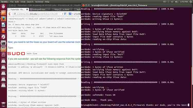
Programming the ATTINY
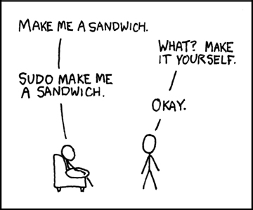
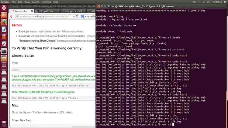
I use ubuntu 12.1 and i just followed the providence tutorial until the "make fuse" step, it returned an error, then me and Ferdinand struggled debugging the traces to check if every path has a micro-solder bridge or if was soldered correctly. Luís sugested to use sudo before the "make fuse" and it worked very well, it hapens that I dont't have administrator permissions to write on my own USB ports. Then i followed the rest of the tutorial and everything went right.
Here, take this nice mnemonic from xKcd
To check if i have the FabISP correctly programmed, i've run lsusb(not isusb, not 1susb), then I had two "multiple vendors USB tiny", I've unpluged the other programmer just to see my FabISP nametag standing alone.