Assignment: redraw the echo hello-world board, add (at least) a button and LED
Open the Eagle tutorial from the fabacademy archive, as a guide for the assignment. First steps are: download Eagle and fab.lbr.
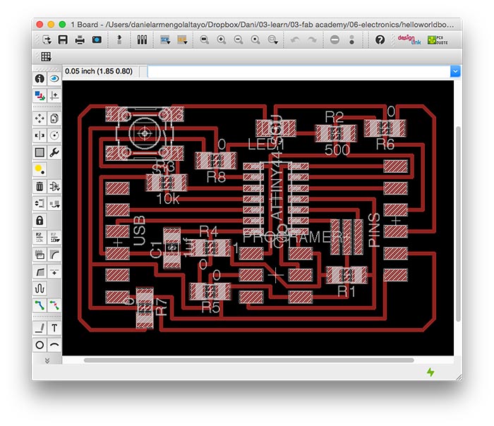
Talking with some classmates I get two inputs that will define my design. Fra wanted to make use of all available free pins on the Attiny, an interesting feature if you want to program new things to the board in the future. Fra makes it possible by opening vias through the board. I wanted to solve the puzzle using only one side of the board. Jani suggested to add a capacitor between VCC to GND to add safety at the circuit.
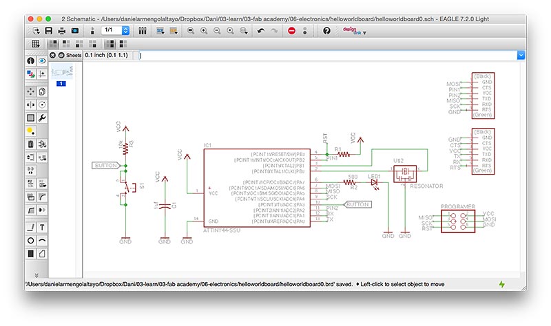
For the schematic design I saw a thirty-minutes tutorial from youtube that our instructor Ferdi sent us. Once I understand how the program works, I start adding components from the list we have in the Eagle tutorial, and this is how it looks my screen after a while.
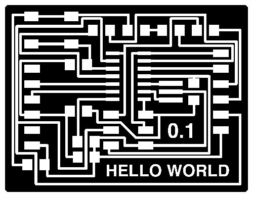
For the board layout I saw another tutorial from the same guy. Everything clear. After more than 10 hours, I have the puzzle solved, using the 0 ohm resistor trick (place a 0 ohm resistor over a trace to hop over an existing trace). This is the board ready to send to the milling machine.
In order to solve the design of the board, I had to add five 0 ohm resistors. This is the schematic updated.
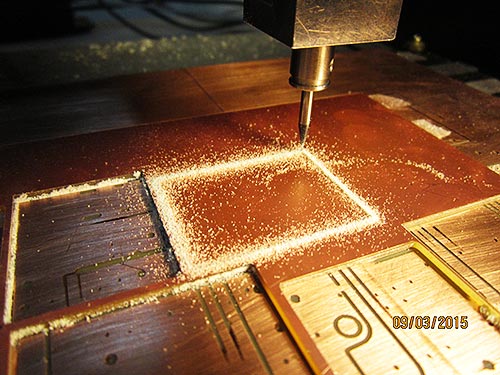
Let's go! It's my turn to use the milling machine, I open the instructions for the FabISP assignment I made two weeks ago, to follow the steps. I set up the machine and check that the PCB is flat and ready to mill, sending the cutout first with the 1/64" mill bit.
So far, so good. I upload the board design to the fabmodules and when I calculate the process I realize that my design is wrong. I have a lot of routes without enough space around to let the mill bit pass.
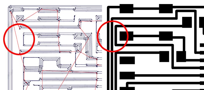
My error, I didn't check the design rules (DRC) in Eagle. Going back to Eagle, this is a close up of my mistake.
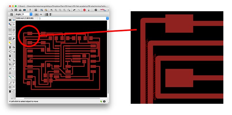
I redraw the board, adding space between the routes and changing the position for some components. The new design increase its size. I add a big hole also, and I remove the text. I check the design rules, and everything is ok.
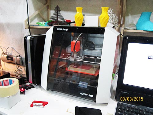
Luckily, at this moment, Ferdi is setting up a second milling machine, the Roland SRM-20 which he teach me how to use to mill my PCB.
There are some parts of the process that are different to the Roland Modela MDX20 I used before, for example, this time I had to use the online version of fabmodules, because the computer connected to this machine is running Windows, save the process there and upload to the program that controls the SRM-20.
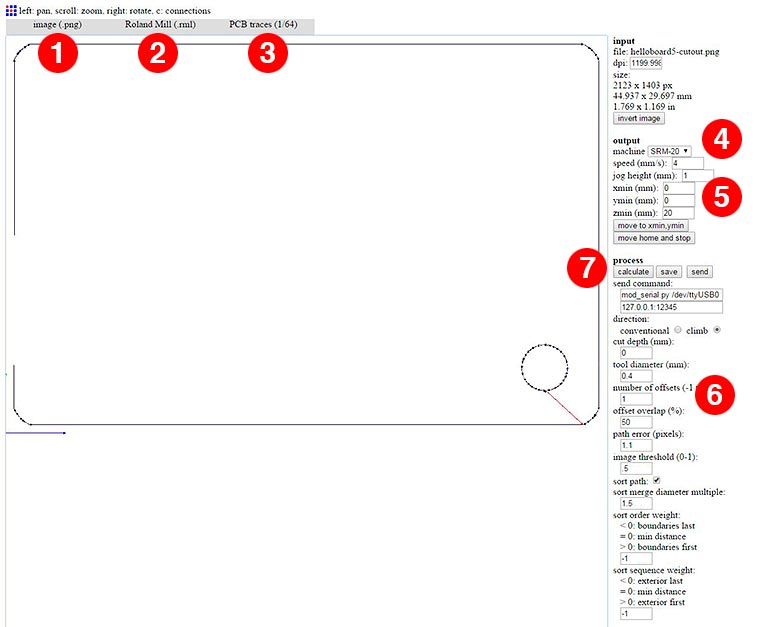
Step by step. Go to fabmodules.org. Upload your png (1). Select "Roland Mill (.rml)" as output format (2). Select "PCB traces (1/64)" as process (3). The output machine is "SRM-20" (4) and make sure that the "xmin" and "ymin" are at 0 (5). "number of offsets" at 1 (6) and you can press "calculate", wait until it finishes and click the "save" button (7).
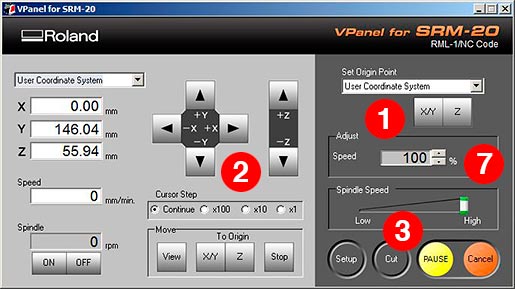
Go to the program "VPanel for SRM-20" and set the coordinates (1) using the arrows and the "cursor step" (2). Start with X and Y, and to setup the Z, move down the end mill close to the surface, and then loose the mill bit letting it fall over the surface (now we are sure that the mill bit is touching the PCB) and tight it again. Set the Z coordinate at the program (1). Click "Cut" (3).
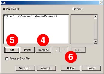
"Delete All" (4), "Add" the file from fabmodules (5) and click "Output" (6). The milling starts. You can change the speed at any moment during the milling (7).
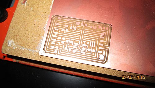
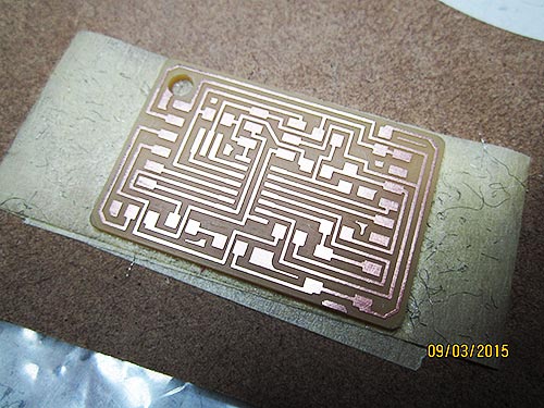
This was the first configuration to check that the PCB is completely flat. Then upload the design of the circuit to fabmodules, repeat the process but change the "number of offsets" to 4. This is how the PCB looks like after the milling.
Third and last iteration with the milling machine. Upload the cutout again to fabmodules, select "PCB traces (1/32)", "cut depth" at 0.5, "stock thickness" at 1.5, "number of offsets" at 1, "calculate" and "save". For the VPanel, the same as before. This is the result.
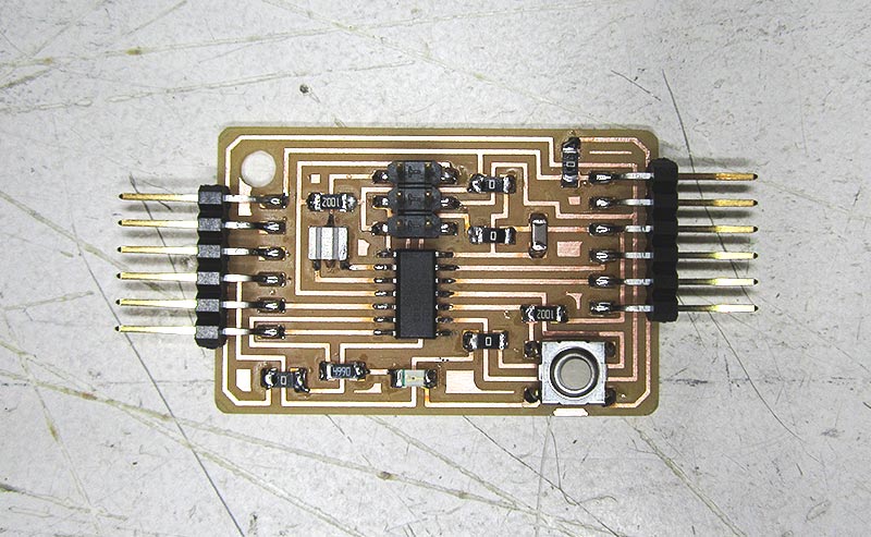
And after soldering.
Excited to see if it works next week!