For this week we carried out the PCB machining process using the Roland Modela Pro II MDX-540. We characterized the design rules for our PCB production process by testing trace widths, spacing, calibration approaches, and machining order — documenting each step and iteration to identify the parameters that produce clean, accurate results.
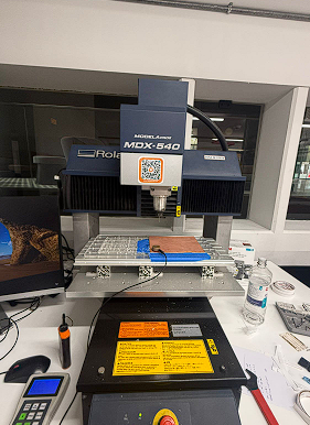
Img 1 — Roland Modela Pro II MDX-540Precision desktop CNC mill used for PCB production. V-Panel controller visible on the left side. Sacrificial bed, copper board, and tool holder in position. Cleaning supplies and touch probe on the right side of the bed.
The MDX-540 is a precision desktop CNC milling machine used to produce PCBs by removing copper from a board surface. It supports engraving (trace isolation), drilling (component holes), and board cutting in a single workflow — making it ideal for rapid in-house PCB prototyping.
⊙
Sacrificial bed
The board is placed on a sacrificial layer that absorbs the final cutting pass, protecting the machine bed from direct contact with the tool.
⌂
Double-sided tape fixturing
Copper boards are fixed using double-sided tape applied to the back surface. The board must be as flat as possible — unevenness directly affects engraving depth consistency.
⌀
Tool — 2 mm V-bit
Engraving was performed with a 2 mm V-bit (40° angle). The V-shape produces cleaner trace isolation than flat end mills at this scale.
Z
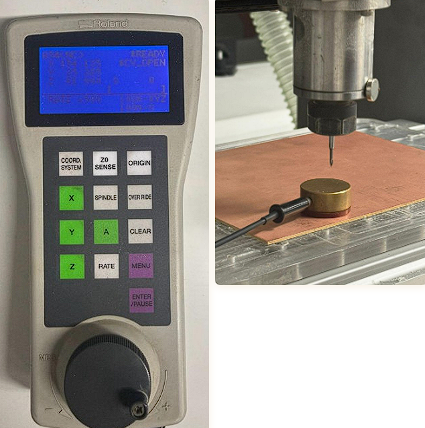
Z0 SENSE calibration
Z-axis height is set using a touch probe sensor. The tool descends until contact is detected — the machine registers that position as the reference height automatically.
Img 12 — V-Panel controller & Z0 SENSE touch probeLeft: Roland V-Panel handheld controller — Z0 SENSE, ORIGIN, SPINDLE, and axis jog buttons visible. Right: 2 mm V-bit tool positioned above the touch probe sensor on the copper board surface during Z-axis calibration.
PCB Materials
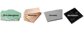
Different substrate materials can be used for PCB production. Each has different mechanical, thermal, and electrical properties that affect its suitability for different applications.
Industry standard material. High mechanical and thermal resistance. Used in most commercial and professional PCBs.
Economical
Phenolic
More affordable than FR-4. Used for simple prototypes. Lower mechanical resistance and not suitable for high-temperature environments.
High-performance
Ceramic
Ideal for high-temperature and high-frequency applications. Excellent thermal stability and electrical insulation.
Thermal
Aluminum
Provides better heat dissipation. Used in power electronics, LED drivers, and applications where thermal management is critical.
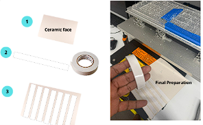
Img 3 — Board preparation — ceramic face & tape fixturingLeft: ceramic-face board components — substrate, double-sided tape roll, and pre-cut strips. Right: applying tape strips to the back of the board before placing it on the machine bed — even tape application is critical for board flatness.
Types of PCB Machining
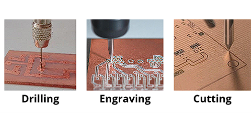
PCB production on the MDX-540 involves three distinct machining processes, each with a specific tool, depth, and purpose. The order in which they are performed is critical to avoid losing precision.
Img 8 — Three PCB machining operationsLeft: Drilling — holes for through-hole component pins. Center: Engraving — V-bit selectively removes copper to isolate traces. Right: Cutting — outline profile cut separates the finished board from the base material.
01
Engraving
The surface copper layer is selectively removed to create the circuit traces. Uses fine V-bit tools at low depth. This step is always done first — if cutting is done first, the board can move and all trace accuracy is lost.
02
Drilling
Holes are made in the board for through-hole components or mechanical fixings. Different drill bit diameters are used depending on the component pin diameter required.
03
Cutting
The board outline is cut, separating it completely from the base material. Always performed last — after engraving and drilling — to keep the board fixed and stable throughout the process.
Machining order matters
Always run engraving first, then drilling, then cutting. Cutting the board outline before engraving releases the board from its fixed position — any movement at that point will ruin the trace alignment and make the board unusable.
Software
G-code Generation — Mods CE
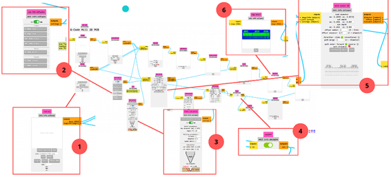
Mods CE is the browser-based CAM tool used to convert the PCB design image (PNG) into G-code for the MDX-540. The workflow connects modules step by step to define the machining parameters and generate a toolpath.
Img 6 — Mods CE — full G-code generation workflowBrowser-based CAM environment with numbered modules: 1 = Read PNG input, 2 = Set PCB defaults (40° V-bit), 3 = Set cut parameters (Cut Z, feed rate), 4 = Calculate toolpath, 5 = Output viewer / NC check, 6 = Send to Roland MDX-540. Arrows show data flow between modules.
1
Read PNG
Load the PNG file of the PCB design. Options: view, invert, flip H/V, rotate 90°. Units: dpi, px, mm, in.
2
Set PCB Defaults
Select the 40° V-bit configuration and define the tool and machining parameters for the job.
3
Set parameters
Define Cut Z depth (-0.112 mm for engraving), feed rate, and spindle speed.
4
Calculate
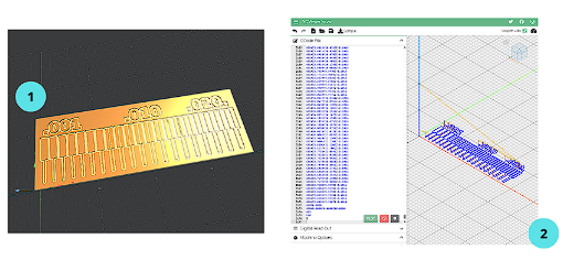
Generate the toolpath. A 3D preview of the machining result is shown before committing to the G-code output.
5
NC Viewer check
Load the G-code into NC Viewer to simulate and verify machining order and cutting behavior before running on the machine.
6
Send to machine
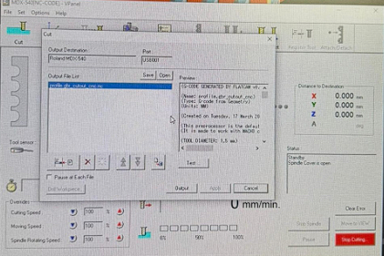
Open VPanel for Modela Pro II, select the G-code file, and start the job. Monitor until completion.
Img 7 — Toolpath preview & NC Viewer simulationLeft (1): Mods CE 3D toolpath preview — orange model shows the PCB with trace isolation paths rendered before G-code is exported. Right (2): NC Viewer simulation — G-code loaded and visualized as blue toolpaths in 3D space, confirming machining order and coverage before sending to the MDX-540.
Img 13 — VPanel for Modela Pro II — G-code file loadedVPanel software interface with the engraving G-code file selected and ready to send. Output destination: Roland MDX-540 (USB001). G-code preview visible on the right. Cutting speed, feed rate, and spindle speed overrides shown at bottom. Job is ready to start.
Step-by-Step Machining Process
Complete workflow from board preparation to final PCB removal, following the order that ensures precision and avoids machining errors.
01
Cleaning and preparation
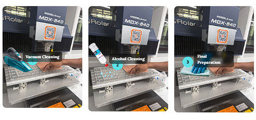
Clean the machine bed with vacuum and alcohol and remove any debris from previous machining processes. A clean surface is essential to avoid precision errors caused by particles under the board.
Img 2 — Bed cleaning — 3 stepsStep 1: Vacuum cleaning — loose chips and debris from previous machining removed with a vacuum. Step 2: Alcohol cleaning — isopropyl alcohol applied to dissolve copper dust and residue from the bed surface. Step 3: Final preparation — bed wiped clean and inspected before placing the copper board.
02
Board preparation
Apply double-sided tape to the back of the copper board. The board must be as flat as possible — any unevenness directly affects engraving depth consistency across the surface.
03
Placing the board
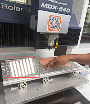
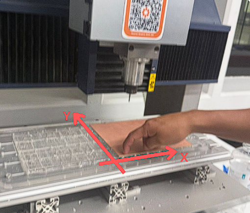
Place the board on the sacrificial layer, ensuring it is well aligned and firmly fixed. Set the origin considering the first quadrant (bottom to top, left to right).
Img 5 — Board placed on sacrificial bedTaped copper board positioned on the MDX-540 bed with the sacrificial layer underneath. Red highlight shows the board area ready for machining. The board is pressed firmly to ensure even contact and eliminate any lift or warp.Img 9 — Setting XY originHand positioning the board under the spindle to define the XY zero point. Red arrows indicate the X and Y axes directions. Origin is set at the bottom-left corner of the board, following the first-quadrant convention (left to right, bottom to top).
04
Z-axis calibration
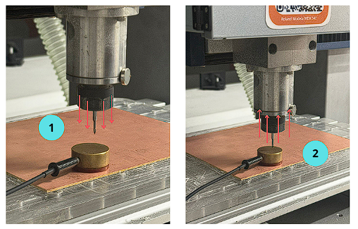
Use the Z0 SENSE option to calibrate the tool height. The tool descends until it contacts the touch probe — the machine automatically registers this position as the Z reference height. Avoid applying extra pressure to the sensor during this step.
Img 10 — Z0 SENSE calibration sequenceLeft (1): Tool descending toward the touch probe sensor — red arrows indicate downward travel. Right (2): Tool making contact with the probe sensor — the machine detects the signal and registers this exact height as Z=0. Light, unpressured contact is critical; excess force shifts the reference and over-engraves the board.
05
Run engraving G-code
Open VPanel, select the engraving G-code file, and start the job. The V-bit removes the copper layer between traces. Monitor the first pass carefully to confirm the depth is correct.
06
Run cutting G-code
After engraving is complete, run the cutting G-code to separate the board from the base material. The sacrificial layer absorbs this final pass.
07
Remove the PCB
Once machining is complete, carefully remove the PCB from the bed using a spatula. Avoid bending or applying lateral force — the board can be fragile along cut edges.
Calibration Tests
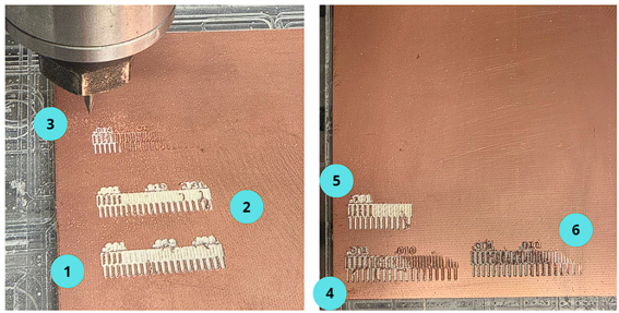
Machining tests were performed using a 2 mm V-bit tool with a Cut Z of -0.112 mm. The results showed that sensor pressure during Z-axis calibration and surface leveling have a direct impact on final machining quality.
Img 11 — Calibration test attempts 1–6 on copper boardLeft panel: attempts 1 (bottom), 2 (center), 3 (top in progress) — showing progressive improvement in engraving quality as sensor pressure was reduced. Right panel: attempts 4 (bottom), 5, 6 (top) — continued refinement of calibration area and technique. Each attempt reveals a specific calibration variable: depth consistency, surface leveling, and sensor contact force.
Attempt 1 — Failed
Excessive sensor pressure
Z-axis calibration was incorrect because too much pressure was applied to the sensor. This caused excessive engraving depth and a poor surface finish.
Attempt 2 — Not optimal
Reduced pressure — still irregular
Sensor pressure was reduced compared to the first attempt. The result improved slightly but the machined finish remained irregular — depth was still inconsistent.
Attempt 3 — Improved
No pressure on sensor
Calibration was performed without applying any pressure to the sensor, obtaining a more accurate height reference. Result improved noticeably.
Attempt 4 — Partial
Different calibration area
The tool was calibrated in a different area of the machine bed. Some parts were still not machined correctly, suggesting surface leveling irregularities across the bed.
Attempt 5 — Stopped
Pressure applied again
Pressure was applied on the sensor again during calibration. The result was not satisfactory and the process was stopped before completion to avoid wasting material.
Attempt 6 — Reference
Best result documented
Final attempt combining correct sensor technique and centered calibration area — used as the reference run for design rule characterization.
Key finding: Z-axis calibration is the most critical variable in PCB engraving quality. Even small differences in sensor contact force directly change the effective engraving depth. The correct technique is to allow the tool to make light, unpressured contact with the sensor and let the machine register the position automatically.
Design Rules Characterized
Parameters confirmed through testing
Trace width and spacing must be defined according to the tool diameter — with a 2 mm V-bit at -0.112 mm Cut Z, the minimum reliable trace isolation requires careful spacing to avoid copper shorts between adjacent traces. Proper Z calibration is essential: even 0.05 mm of excess depth can over-engrave and cut through thin trace widths. Surface flatness of the board directly limits how consistent engraving depth is across the full PCB area.
Individual Reflections
What each team member learned from this week's assignment.
Nicolas
Understanding the design rules through five calibration attempts was far more instructive than any single successful run would have been. Each failed attempt revealed a specific cause — excessive sensor pressure, surface irregularities, wrong calibration area — and forced me to think about which variable had changed between attempts. The most important lesson was that Z-axis calibration is not just a setup step: it is the parameter that everything else depends on. Trace width and spacing are defined in the design, but their physical outcome is entirely determined by how accurately the Z reference is set. Seeing a design rule fail in hardware, and then understanding exactly why, made the concept stick in a way a datasheet never could.
Micaela
Working with Mods CE and NC Viewer showed me how important it is to verify a toolpath before committing to the machine. The simulation step in NC Viewer caught issues in machining order that would have been expensive in time and material to discover mid-job. I also learned that the board preparation steps — cleaning the bed, applying tape evenly, keeping the board flat — are not just housekeeping: they are precision variables. A board with a small warp produces an inconsistent engraving depth across the surface, and no amount of calibration fixes a board that is not flat to begin with.