Week 6 Progress Checklist
| Status | Task |
|---|---|
| ✓ | Linked to the group assignment page |
| ✓ | Documented what you have learned in electronics design |
| ✓ | Checked your board can be fabricated |
| ✓ | Explained problems and how you fixed them |
| ✓ | Included original design files (Eagle, KiCad, etc.) |
| ✓ | Included a ‘hero shot’ |
Electronics Design
Group Assignment
Circuit Test
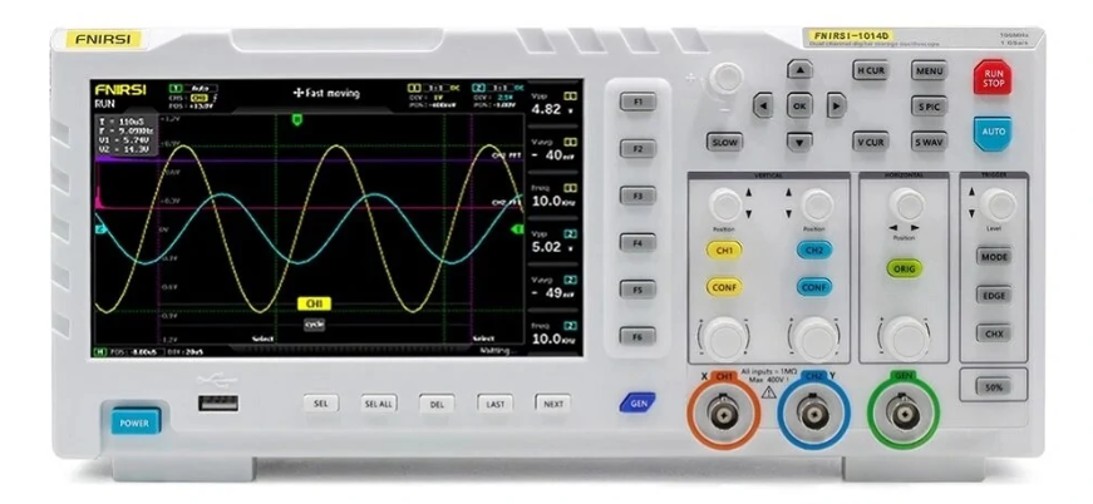
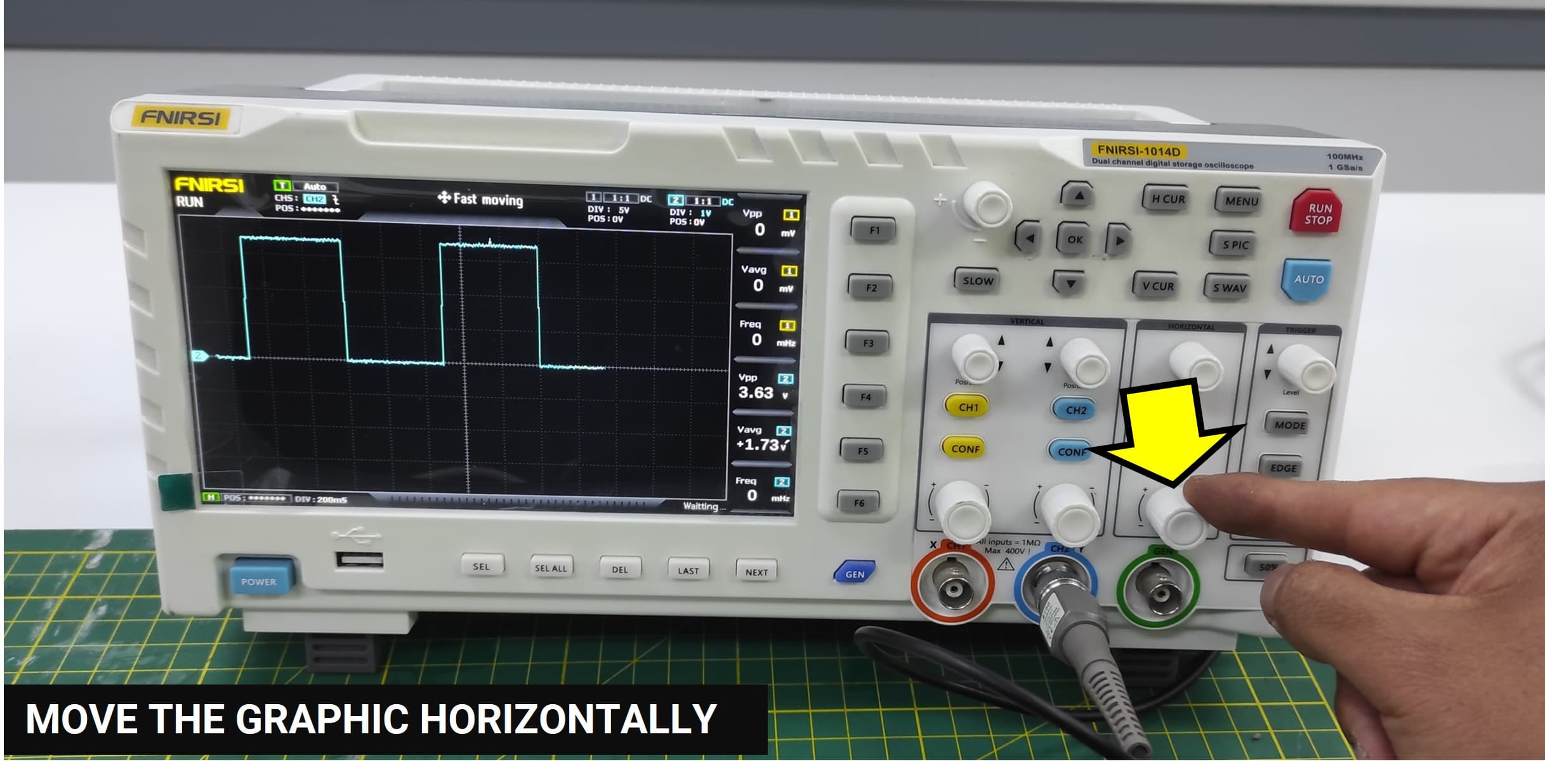
Osciloscope
An oscilloscope is an electronic test instrument used to measure and visualize electrical signals. It displays voltage signals as waveforms on a screen, showing how the signal changes over time. With an oscilloscope, you can observe important characteristics of a signal such as amplitude (voltage level), frequency, period, rise and fall time, and noise. This makes it very useful for analyzing circuits, debugging electronic systems, and verifying signal integrity.
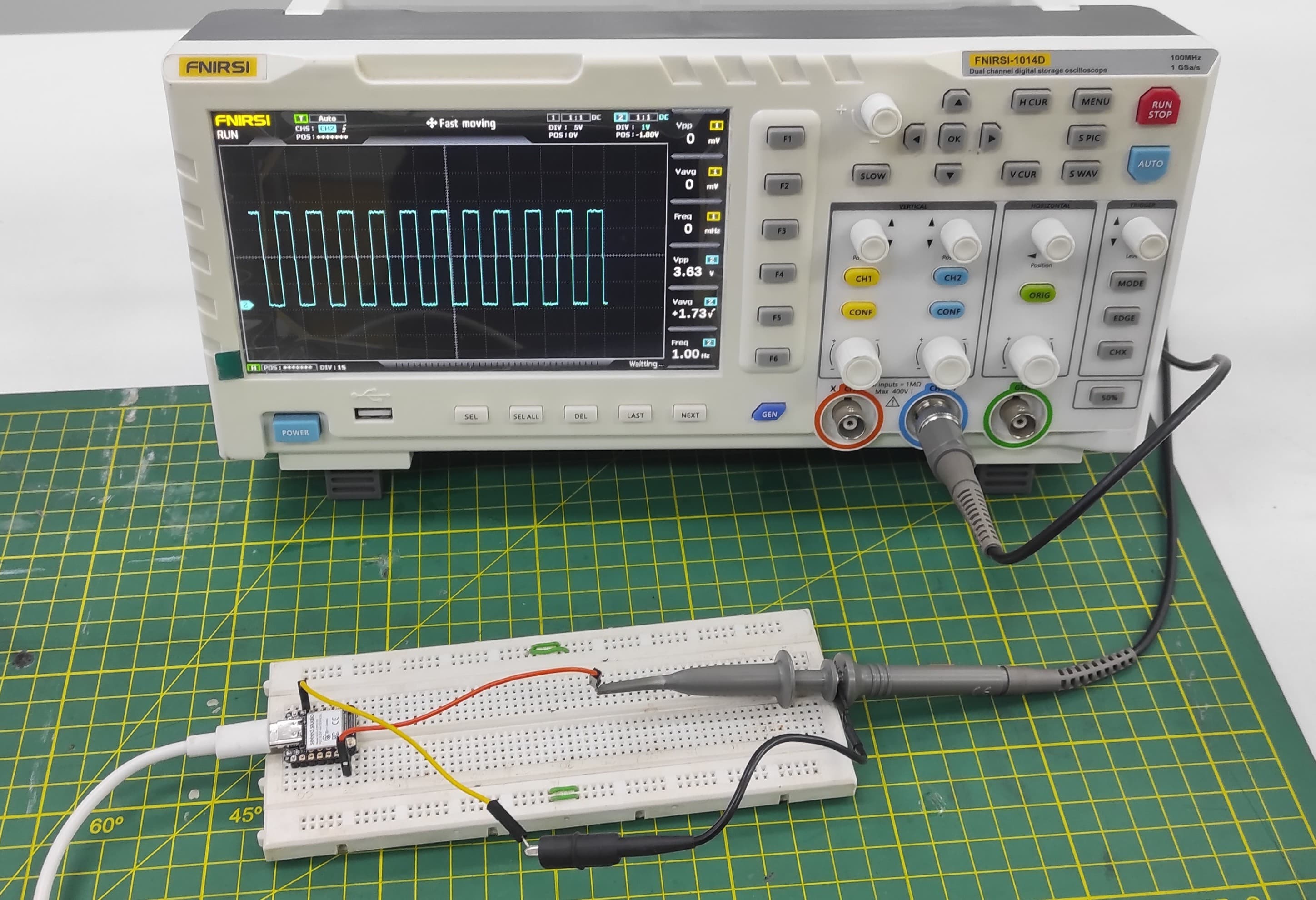
To observe a signal on the oscilloscope, I will demonstrate how a blink code works and how it appears on the oscilloscope. We will start by connecting pin 6 to the oscilloscope channel and the GND pin to the oscilloscope ground. Finally, we will observe the blink code in action.
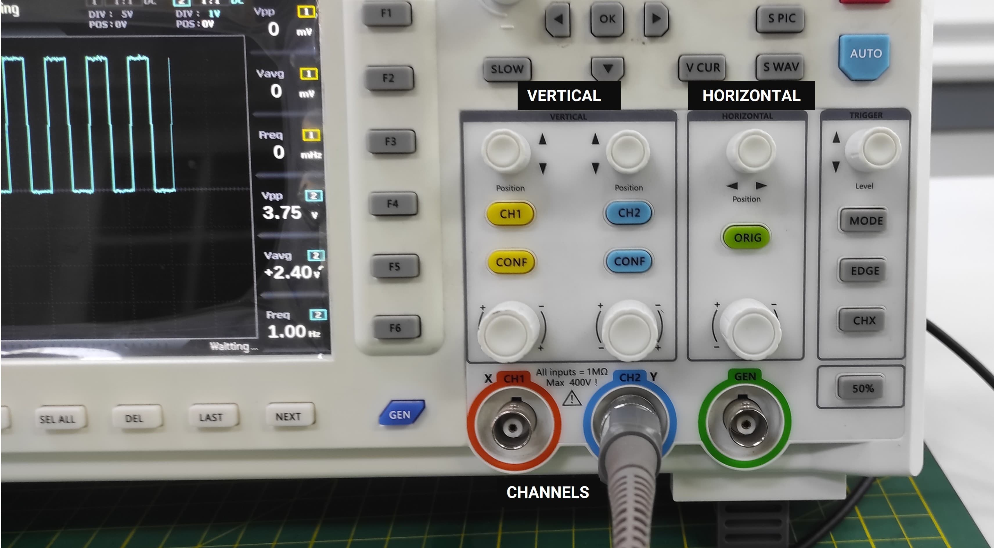
There are several controls on the oscilloscope. The vertical control allows us to move the waveform vertically, and the horizontal control lets us scale the waveform horizontally. This helps us see the signal more clearly.
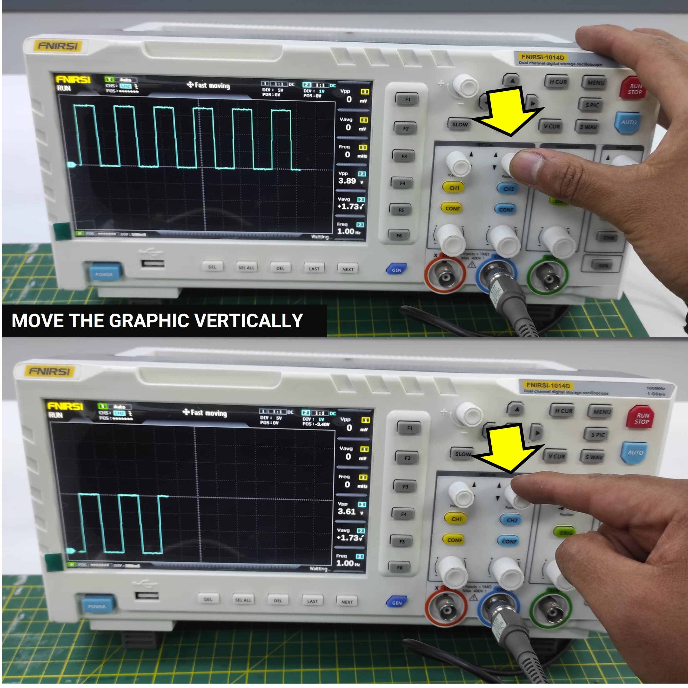
By rotating the vertical control on the oscilloscope, the waveform can be shifted vertically, as illustrated in the image below.
When we rotate the horizontal control of the oscilloscope, we can adjust the horizontal division on the oscilloscope.
Individual Assignment
Electronics Design
Altium Designer - EDA Software
For PCB design, I utilize Altium Designer, a professional electronics design software for schematic capture and layout..
Altium Designer is a professional software application used for electronic design automation (EDA) . It is primarily used by engineers to design printed circuit boards (PCBs) , allowing them to create the schematic (circuit diagram), layout the physical board, and generate the files needed for manufacturing.
You can download Altium Designer from the official website: Altium Designer
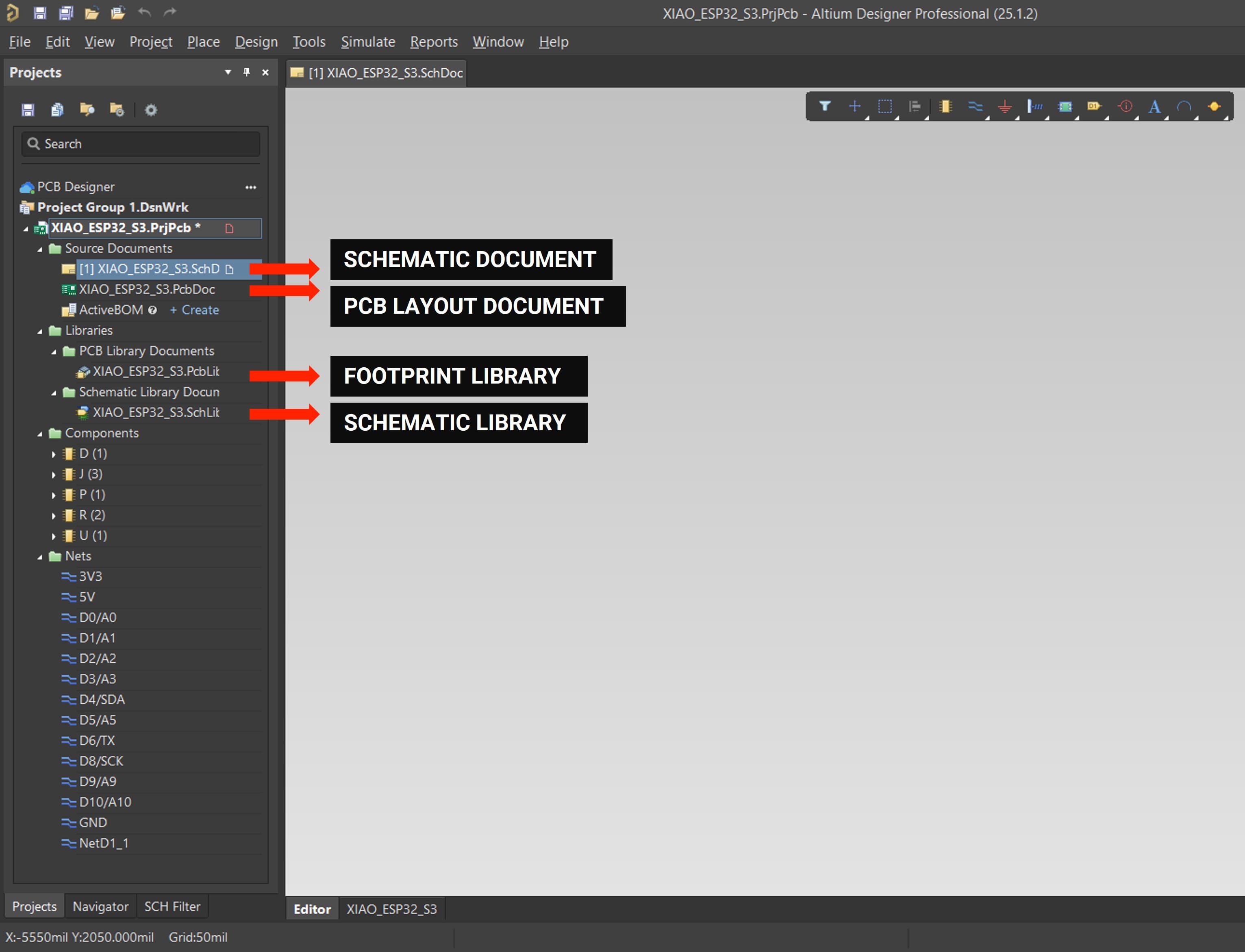
I started by creating the project. Then, I set up the required libraries, including the schematic library and the footprint library. After that, I created both the schematic document and the PCB layout document.
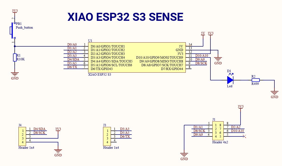
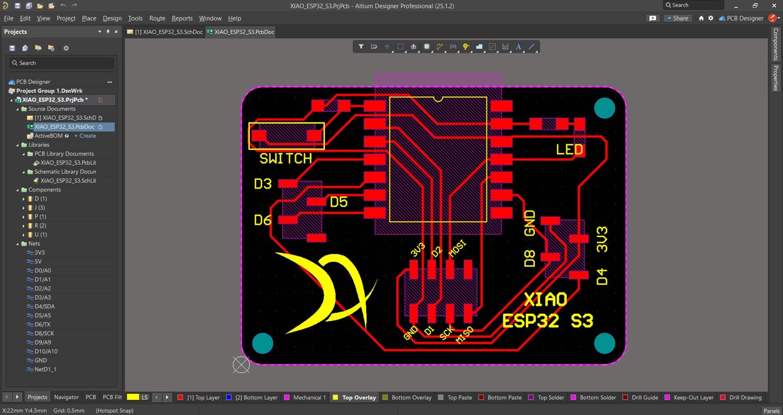
After that, I created the schematic circuit. I used one LED diode as an output to indicate the system status and one switch as an input for user interaction. In addition, I added header pins to break out and access the SPI and I2C interfaces from the XIAO ESP32 S3, making it easier to connect external modules and peripherals in the future.
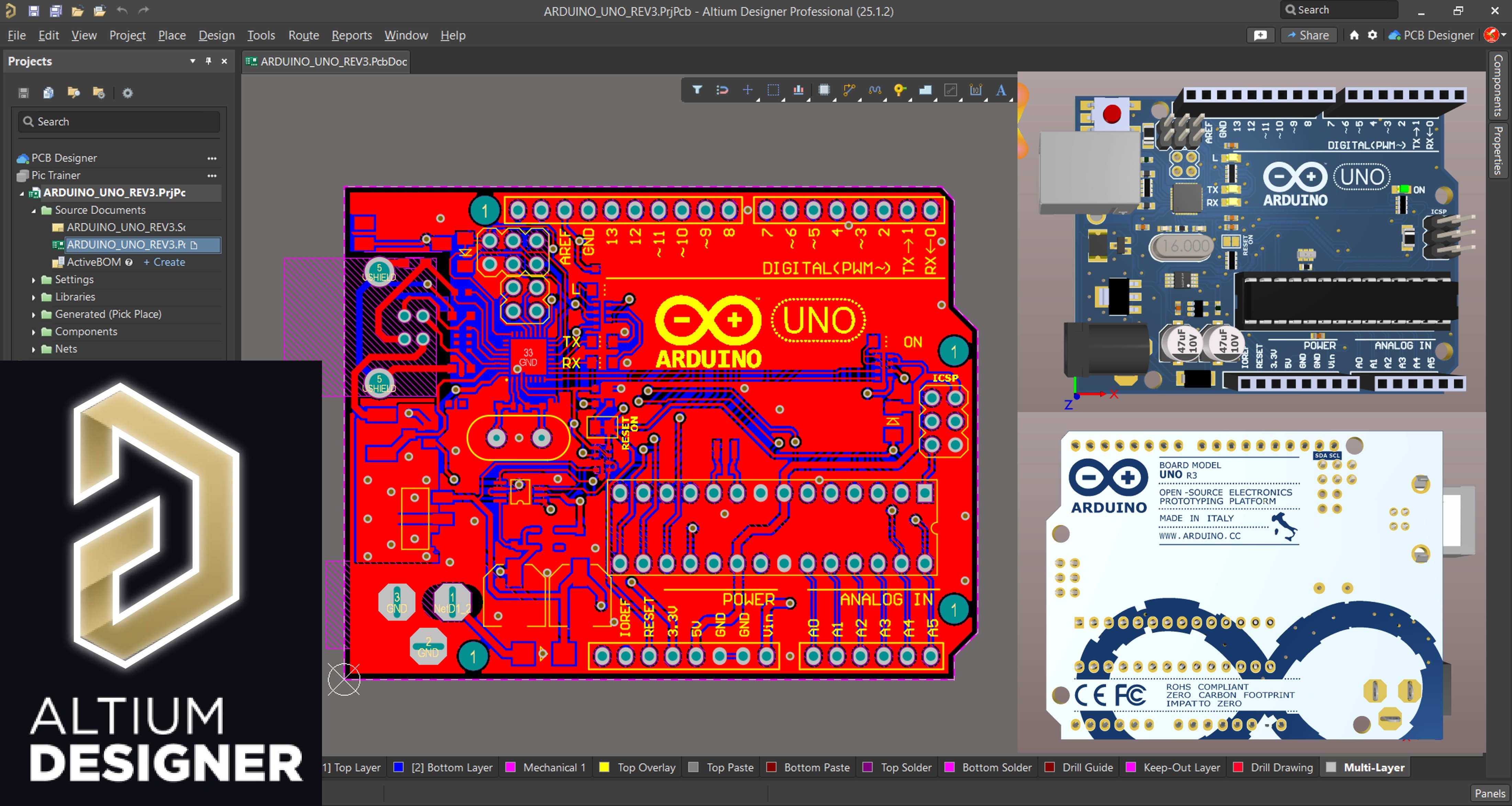
After completing the schematic, I moved on to the PCB layout design. During this stage, I carefully arranged the components on the board, placing them as close as possible to their corresponding pins on the microcontroller. This approach helped minimize the length of the tracks, which reduces signal interference, improves overall performance, and makes the routing process cleaner and more efficient. I also aimed to keep the layout organized and compact to ensure better space utilization and a more professional final design.
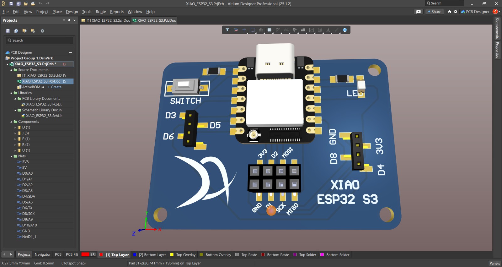
Altium Designer also offers a 3D view feature, which allows designers to visualize the PCB in a realistic three-dimensional environment. This feature helps in checking the physical appearance of the board, verifying component placement, and ensuring that there are no mechanical conflicts between parts. Using the 3D view, I was able to inspect the overall layout more clearly, confirm the alignment of components, and evaluate the board’s final look before manufacturing. It also helps in detecting potential height issues or spacing problems, making the design process more accurate and reducing the risk of errors during production.
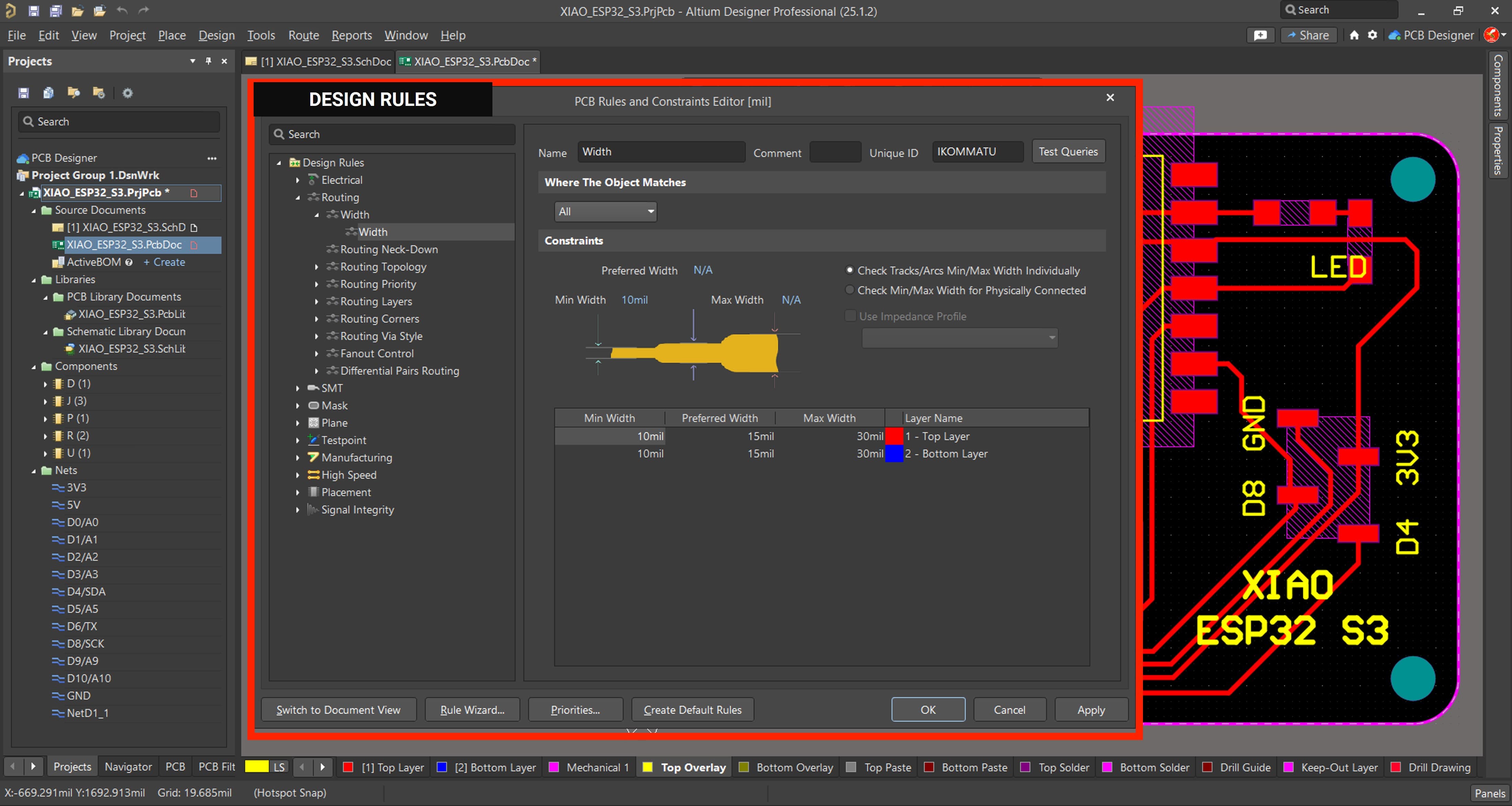
In the design rules for routing, I set the trace width to 15 mil. Using a 15 mil trace width also made the routing process smoother and more consistent, especially for power and signal lines. Overall, this setting worked well for the requirements of my design and contributed to a clean and robust PCB layout.
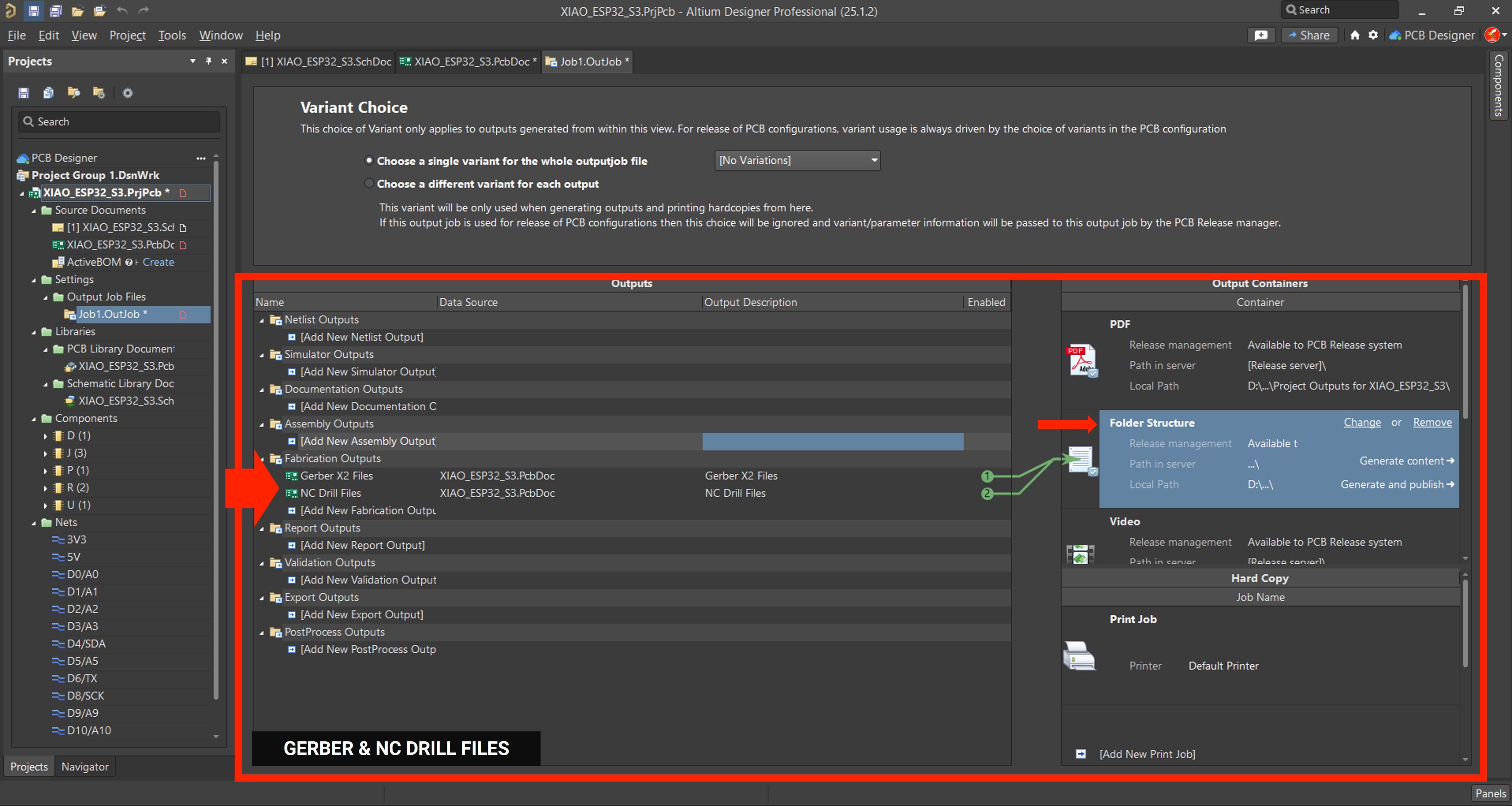
After finalizing the PCB layout and checking the design rules, I exported the Gerber files along with the NC drill files, which include all the necessary manufacturing data such as copper layers, solder mask, silkscreen, board outline, and drilling details. With these files properly generated and verified, the design was fully prepared and ready to be sent to the manufacturer for fabrication.
8. Learnings
Through this process of 3D scanning with the Go!SCAN 20 and integrating it with 3D printing, several important lessons were learned. First, calibration is a critical step that must be performed before each scanning session using the included kit, as it directly impacts the accuracy of the captured data. The real-time preview feature in the VXelements software proved to be invaluable, allowing immediate feedback and the ability to correct missing areas during scanning.
Additionally, designing a test sample holder in Onshape with infill percentages ranging from 0% to 100% provided an effective visual demonstration of how infill affects print strength, weight, and material usage. This simple model became a useful teaching tool for understanding infill properties in 3D printing.
9. Files
Here are the files available for download.