Week 17 Progress Checklist
| Status | Task |
|---|---|
| ✓ | Documented the workflow(s) and process(es) you used |
| ✓ | Explained how your process is not covered in other assignments |
| ✓ | Described problems encountered (if any) and how you fixed them |
| ✓ | Included original design files and source code |
| ✓ | Included ‘hero shot’ of the result |
Wildcard Week
PCB Fabrication with Fiber Laser
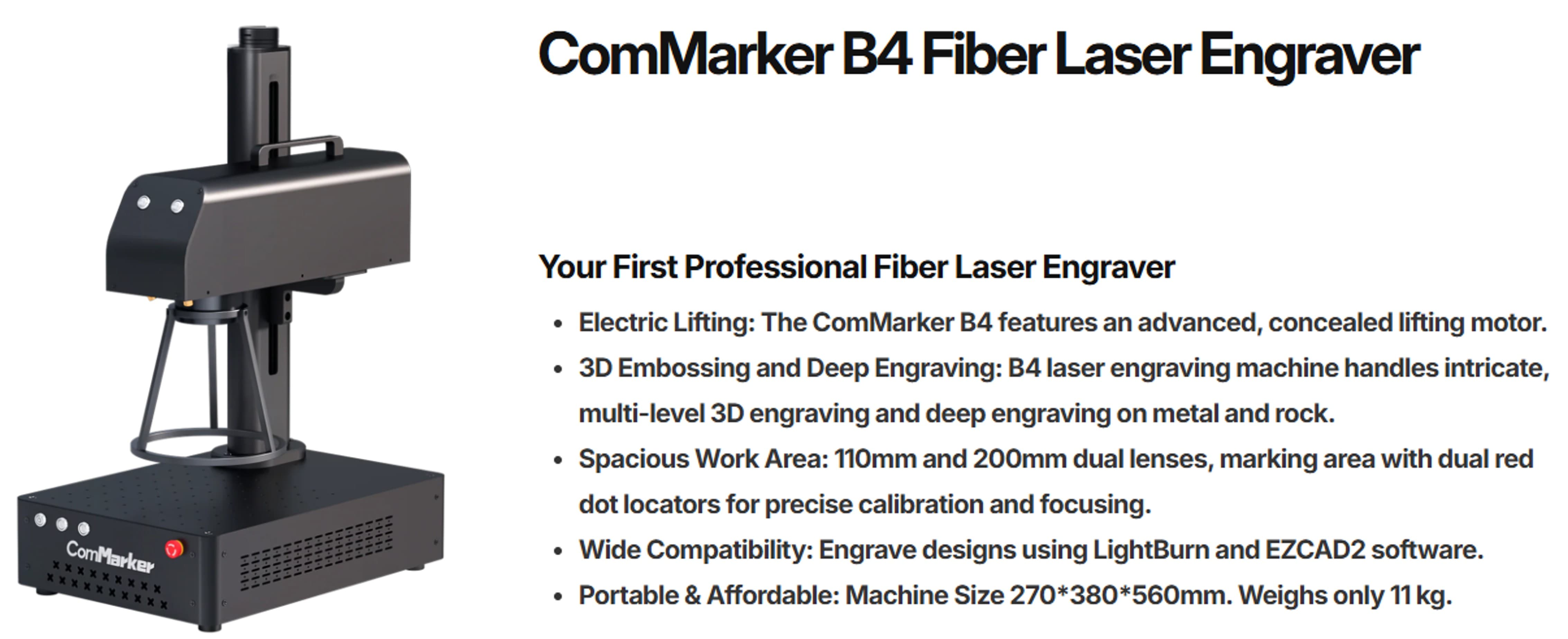
1. ComMarker B4 Fiber Laser Engraver
The ComMarker B4 Fiber Laser Engraver is a compact and powerful laser engraving machine designed for high-precision marking on metal and select non-metal materials. It features fast engraving speeds, fine detail accuracy, and reliable performance, making it ideal for custom jewelry, tools, electronics, industrial parts, and personalized gifts. With its user-friendly software support and durable fiber laser technology, the B4 is suitable for both hobbyists and professional makers.
ComMarker B4: Official Website
2. PCB Board to manufactur with Fiber Laser
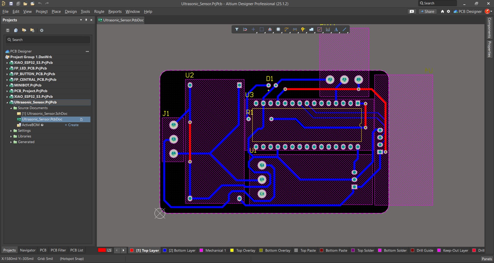
I designed a PCB using basic components, including an Arduino Nano and an ultrasonic sensor, mainly to test the PCB manufacturing process rather than the functionality of the circuit itself.
For PCB manufacturing, we need the Gerber files, which contain all the necessary design data required to fabricate the board.
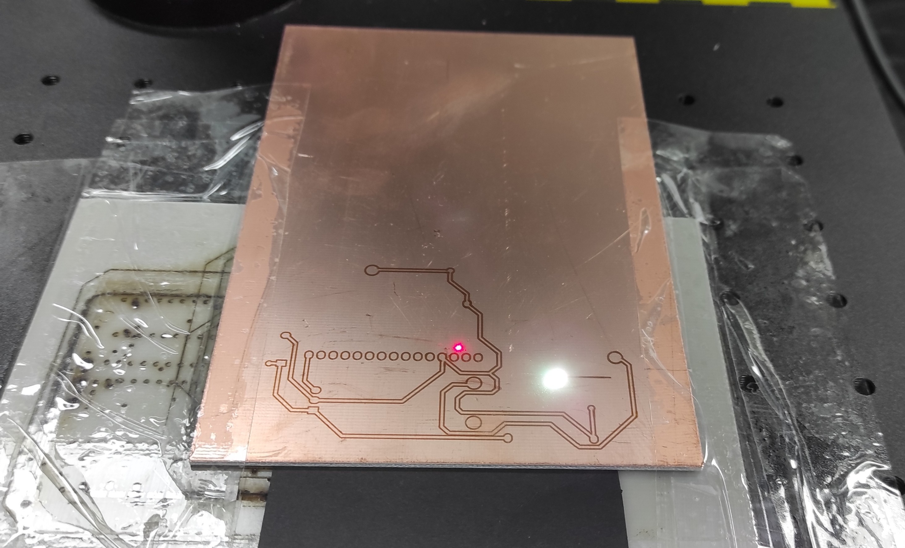
3. Manufacturing the PCB
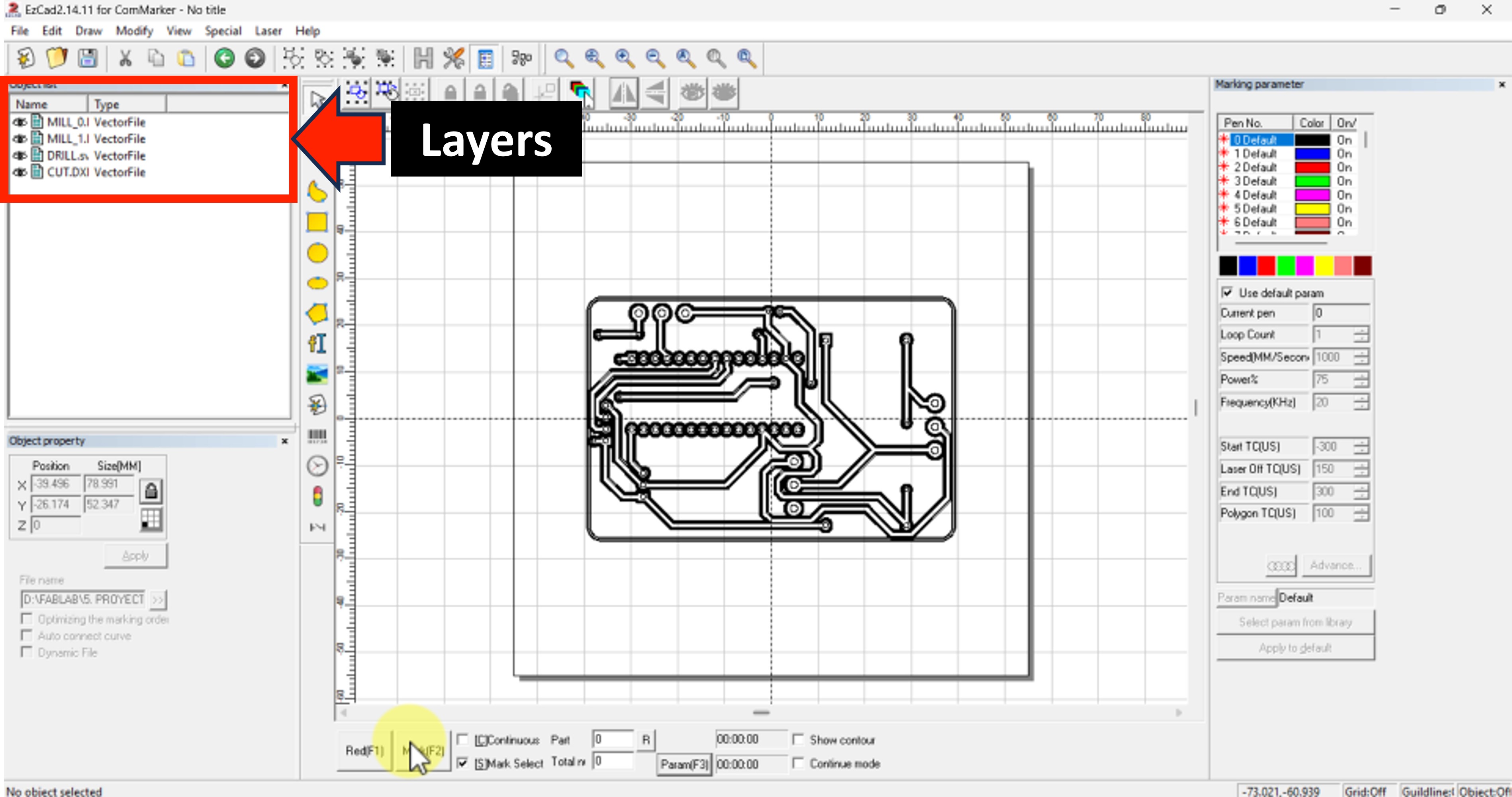
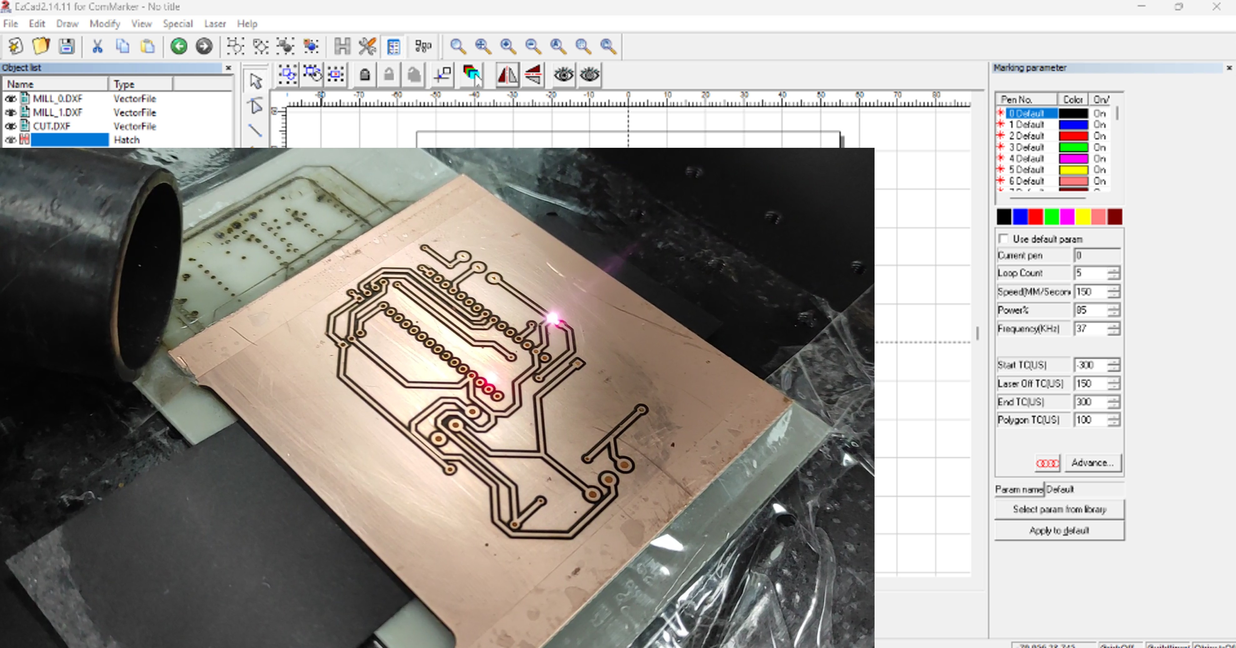
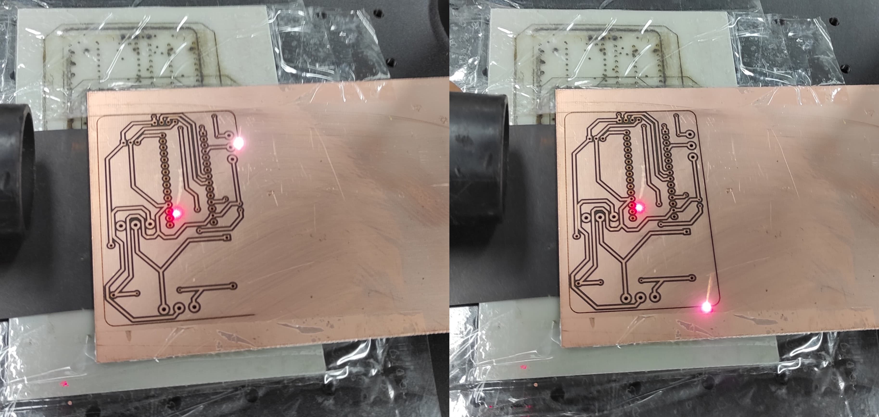
In order to start the process, first we need to open our files on the Ezcad Software.
More about Ezcad: Official Website
Once we opened EZCAD, we needed to import the required files — in this case, the PCB top layer, the drill files, and the board outline (border).
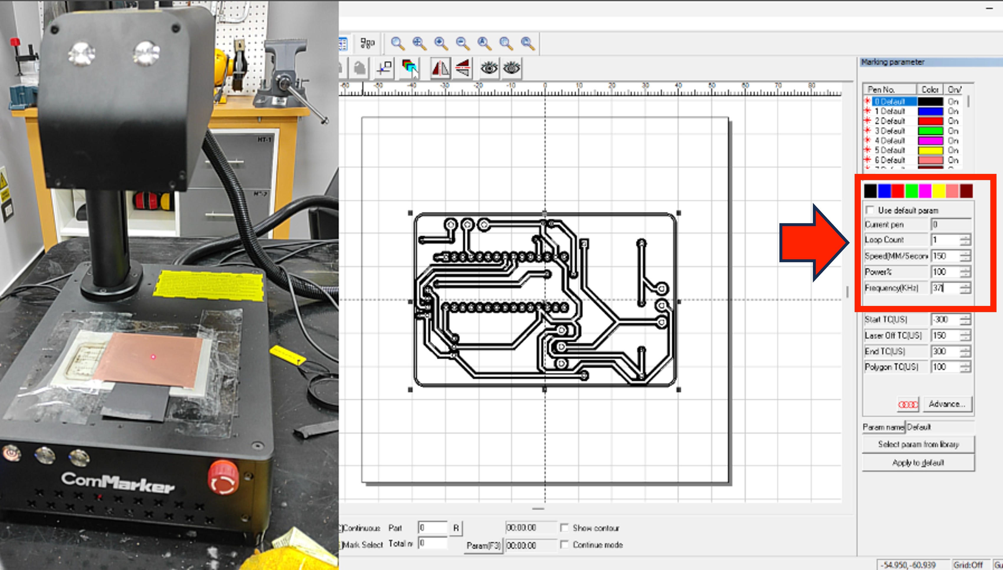
The first layer we worked on was the top copper layer. The parameter values we used are shown below. Speed:150, Power:100, Frequency:37
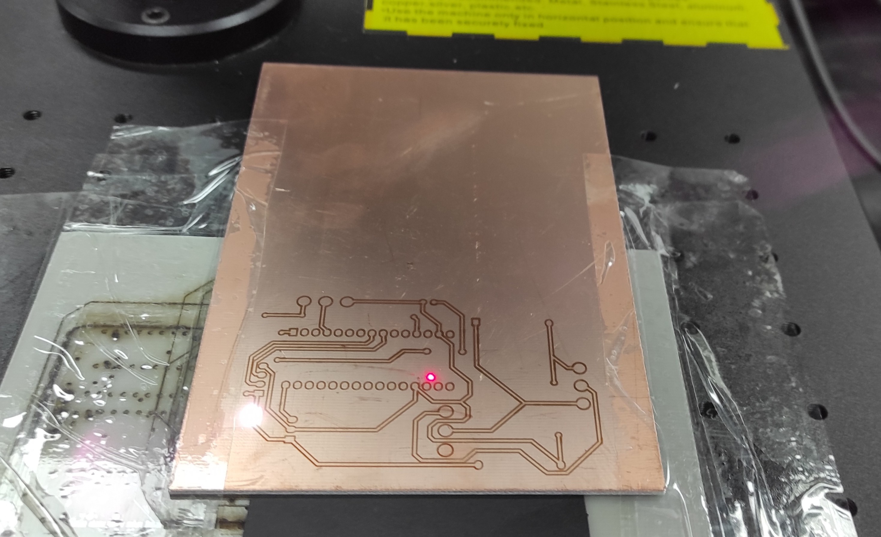
The next layer we need to work on is the drill layer.The parameter values we used are shown below. Speed:150, Power:85, Frequency:37
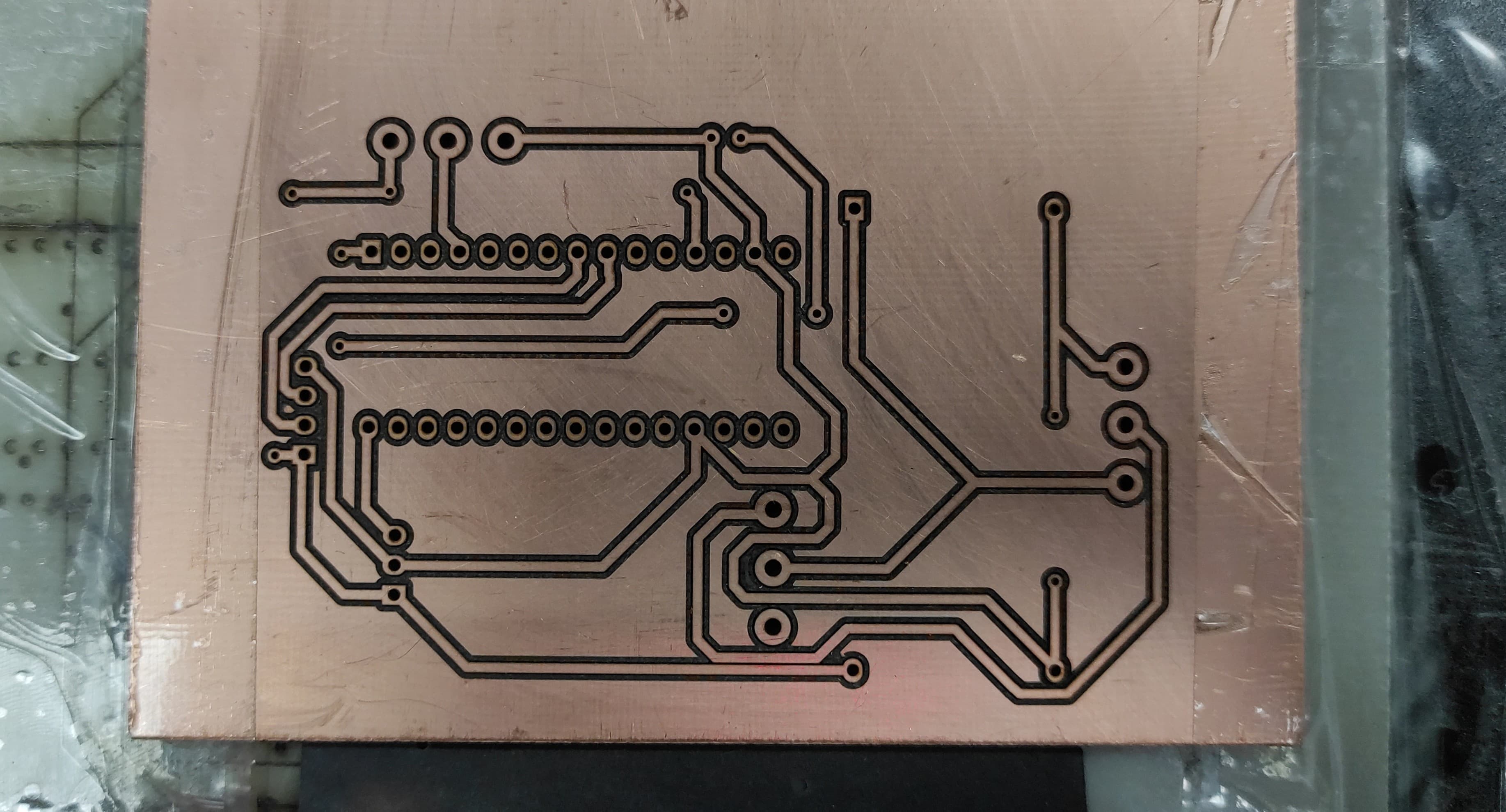
Finally We need to cut the border of the PCB.The parameter values we used are shown below. Speed:30, Power:100, Frequency:37
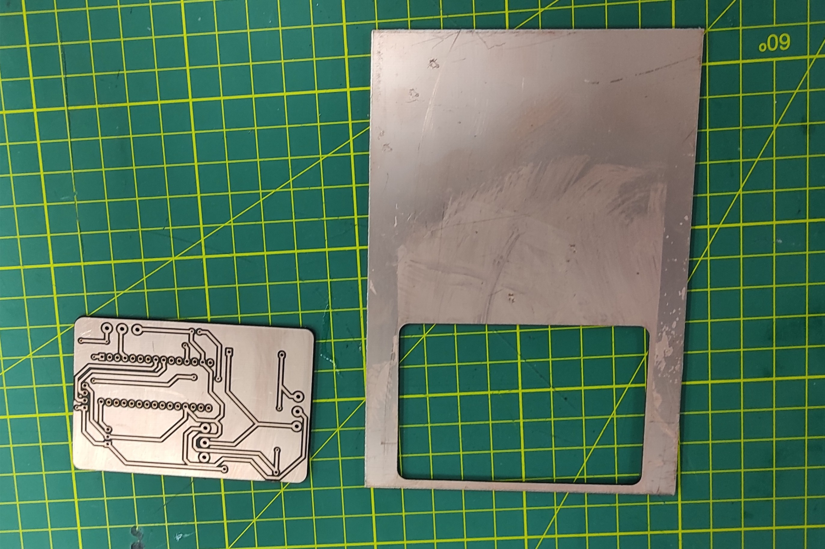
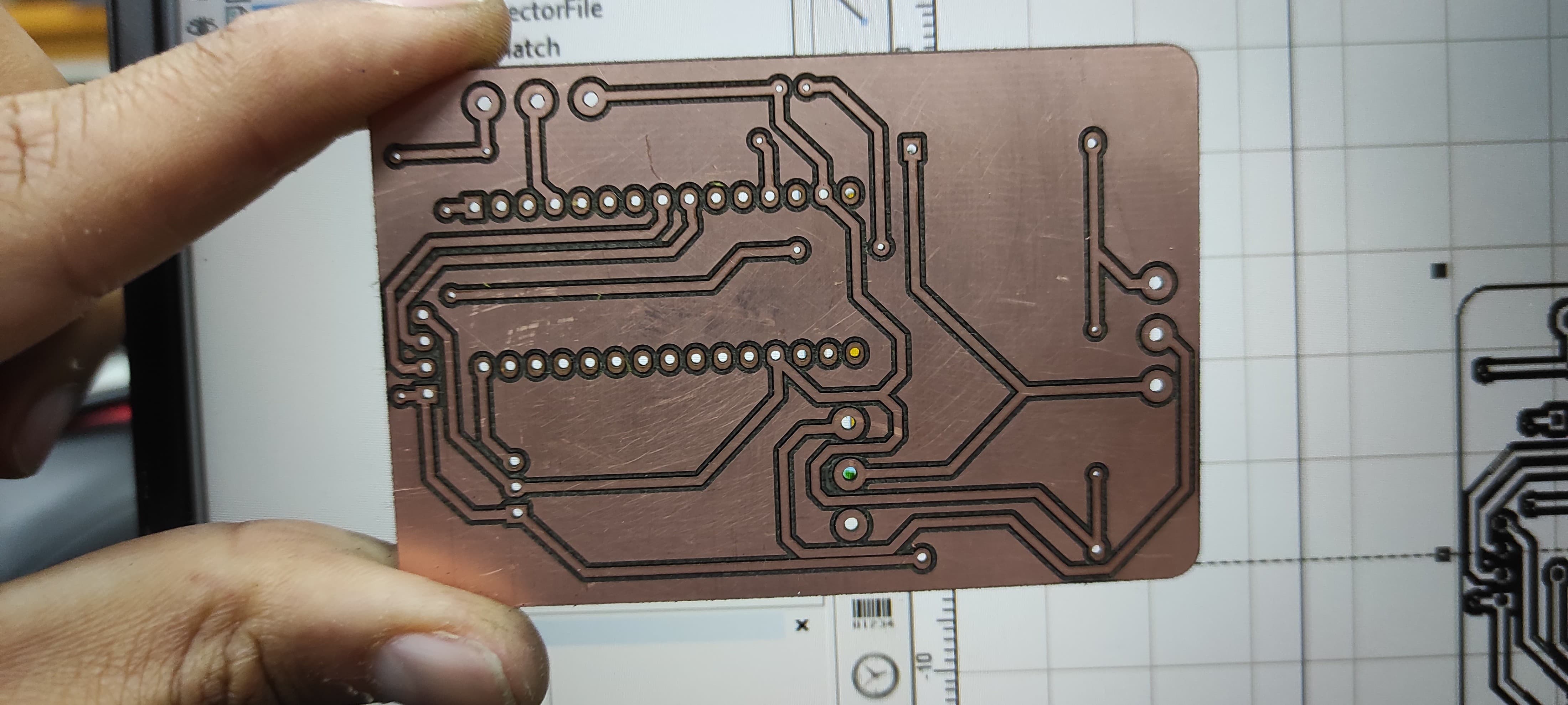
4. Final Result
After all the steps, we have our PCB ready to be soldered.
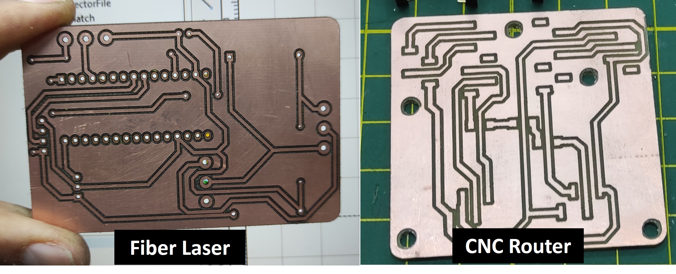
5. Comparison of Fiber Laser vs. CNC Router Techniques for PCB Manufacturing
I compared both methods to gain a better understanding of the advantages and limitations of using Fiber Laser technology versus CNC technology for PCB fabrication.
| Nro | Aspect | Fiber Laser PCB Fabrication | CNC Router PCB Fabrication |
|---|---|---|---|
| 1 | Precision | Very high precision, capable of producing fine traces and small features. | Good precision, but limited by tool diameter and machine accuracy. |
| 2 | Minimum Trace Width | Can achieve very narrow traces and spacing , for this pcb I used 15 mill track thickness. | Usually limited to in my case around 25 mill track thickness. |
| 3 | Tool Wear | No physical tool wear since material is removed by the laser. | Cutting tools wear over time and must be replaced periodically. |
| 4 | Hardware Integration | Connect the control board and power board. | Correct electrical integration. |
| 5 | Speed | Fast for intricate designs and small features. | Faster for simple designs but slower for highly detailed patterns. |
| 6 | Material Contact | Non-contact process, reducing mechanical deformation. | Contact process that can introduce vibration and mechanical stress. |
| 7 | Cost | Higher initial investment and maintenance costs. | Lower equipment cost and generally lower operating costs. |
| 8 | Debugging & Optimization | Fix issues and improve performance. | Optimized and stable prototype. |
| 9 | Holes | Takes time for making the holes . | Faster for making the holes . |
6. Learnings
It is very important to properly adjust the laser focus; otherwise, the dimensions of the engraved PCB may differ from those of the original design file. The drilling process is also the most time-consuming part, so it is necessary to repeat it more than once to ensure that all the holes are properly completed.
7. Files
Here are the files available for download.