WEEK 06
Electronics Design
Group assignment:
- Use the test equipment in your lab to observe the operation of a microcontroller circuit board (as a minimum, you should demonstrate the use of a logic analyzer).
- Document your work on the group work page and reflect what you learned on your individual page.
What I Learned From Teamwork
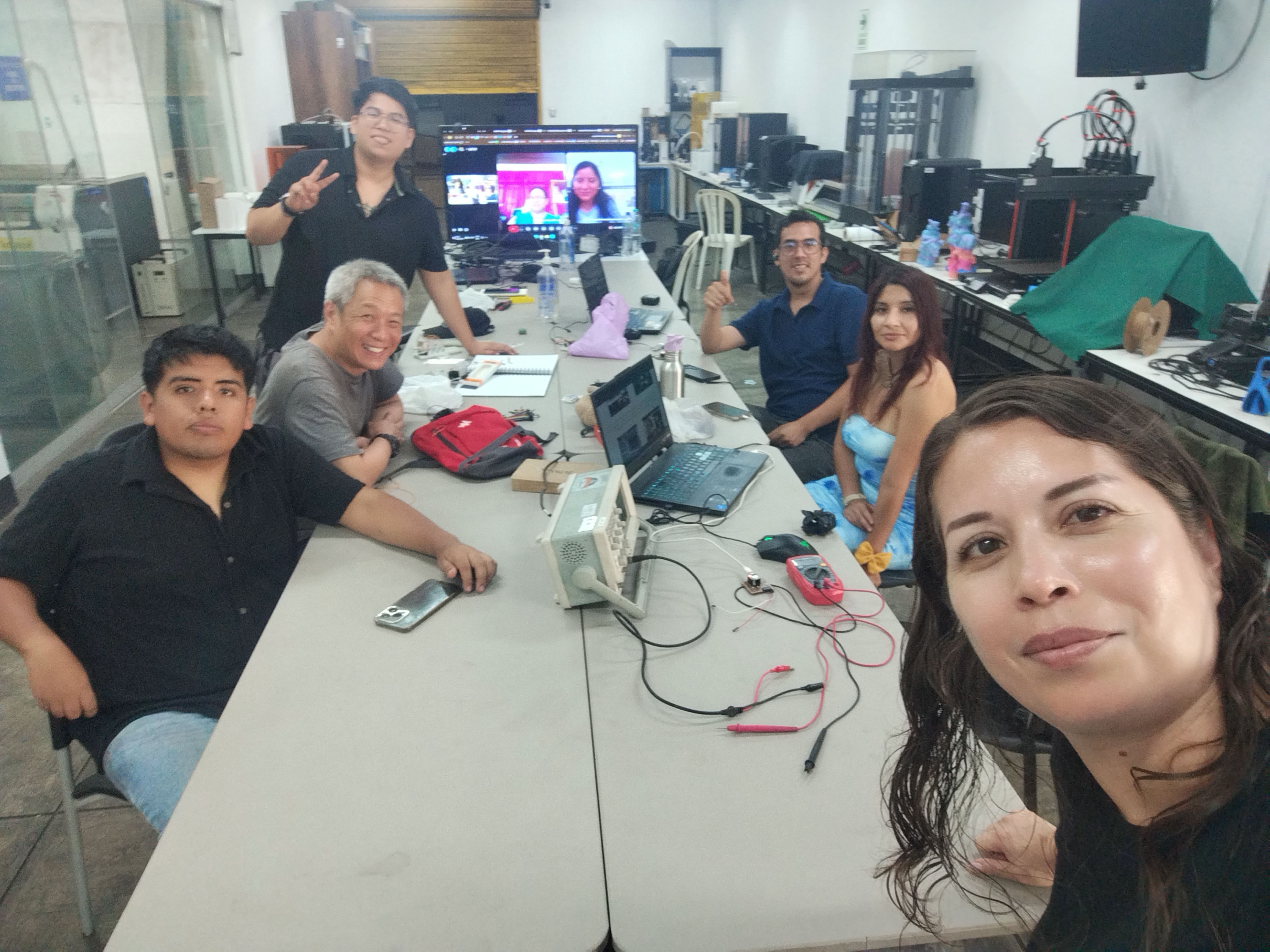
Equipment Used
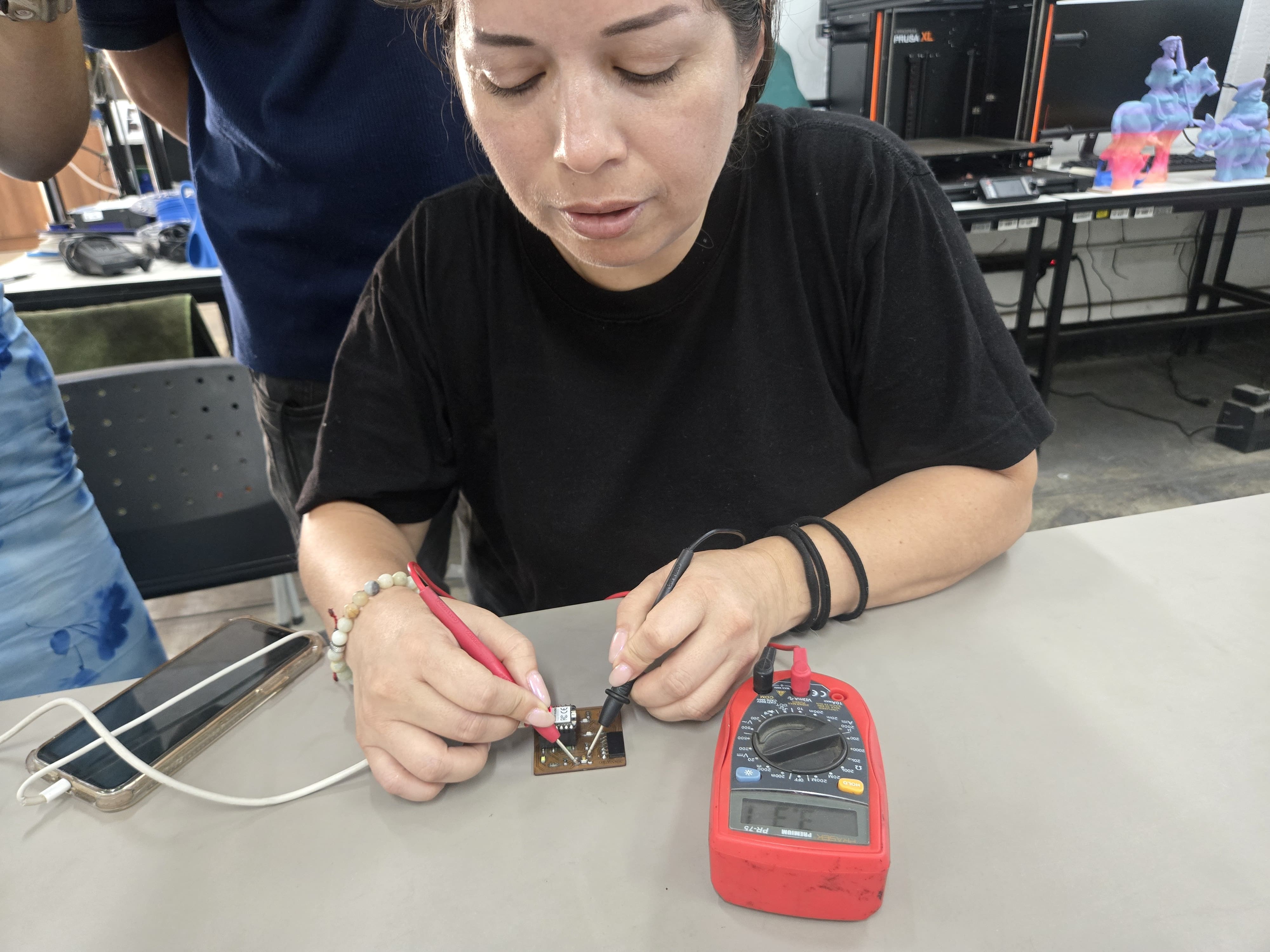
For this group task we used the following laboratory equipment::
Digital Multimeter (PR-75)
Main features:
- DC voltage measurement up to 600V.
- AC voltage measurement up to 600V.
- Resistance measurement (Ω)
- Continuity test with buzzer.
- Diode test.
- Digital LCD display.
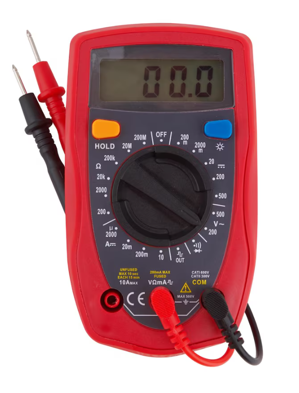
Use in group practice:
It was used to verify power supply (3.3V and 5V), check continuity between tracks and rule out short circuits before taking measurements with the oscilloscope.
Microcontroller board: Custom PCB with Seeed Studio XIAO RP2040.
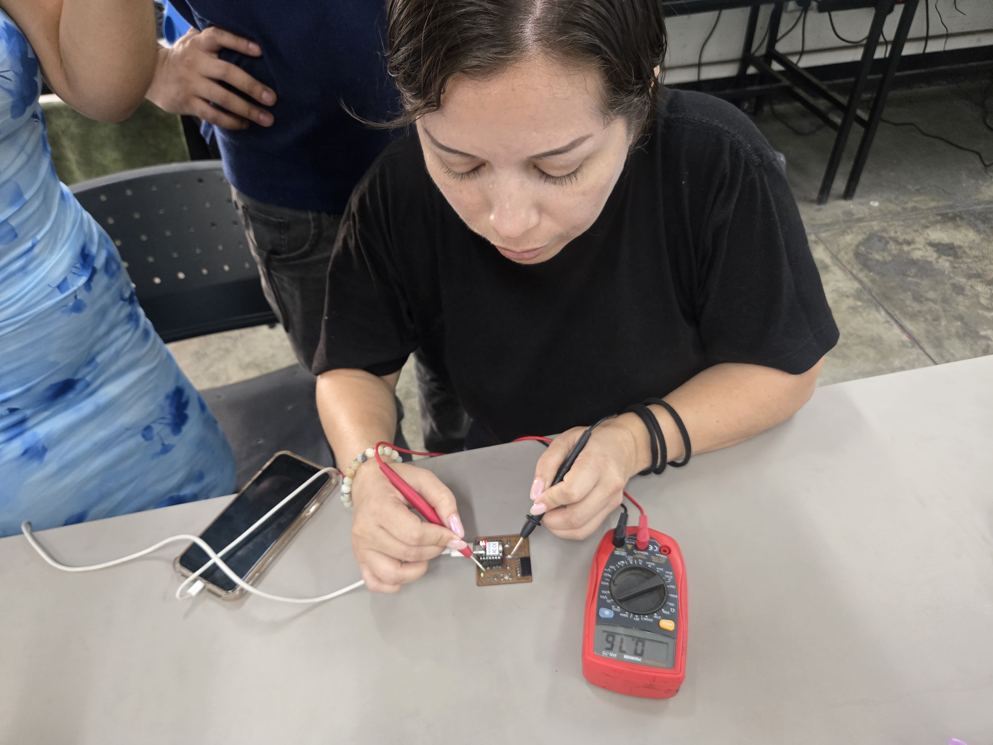
The continuity signal of the PCB traces was verified, from where it comes out of the pin to where it reaches an output, guided by the sound of the buzzer since this multimeter does have one.
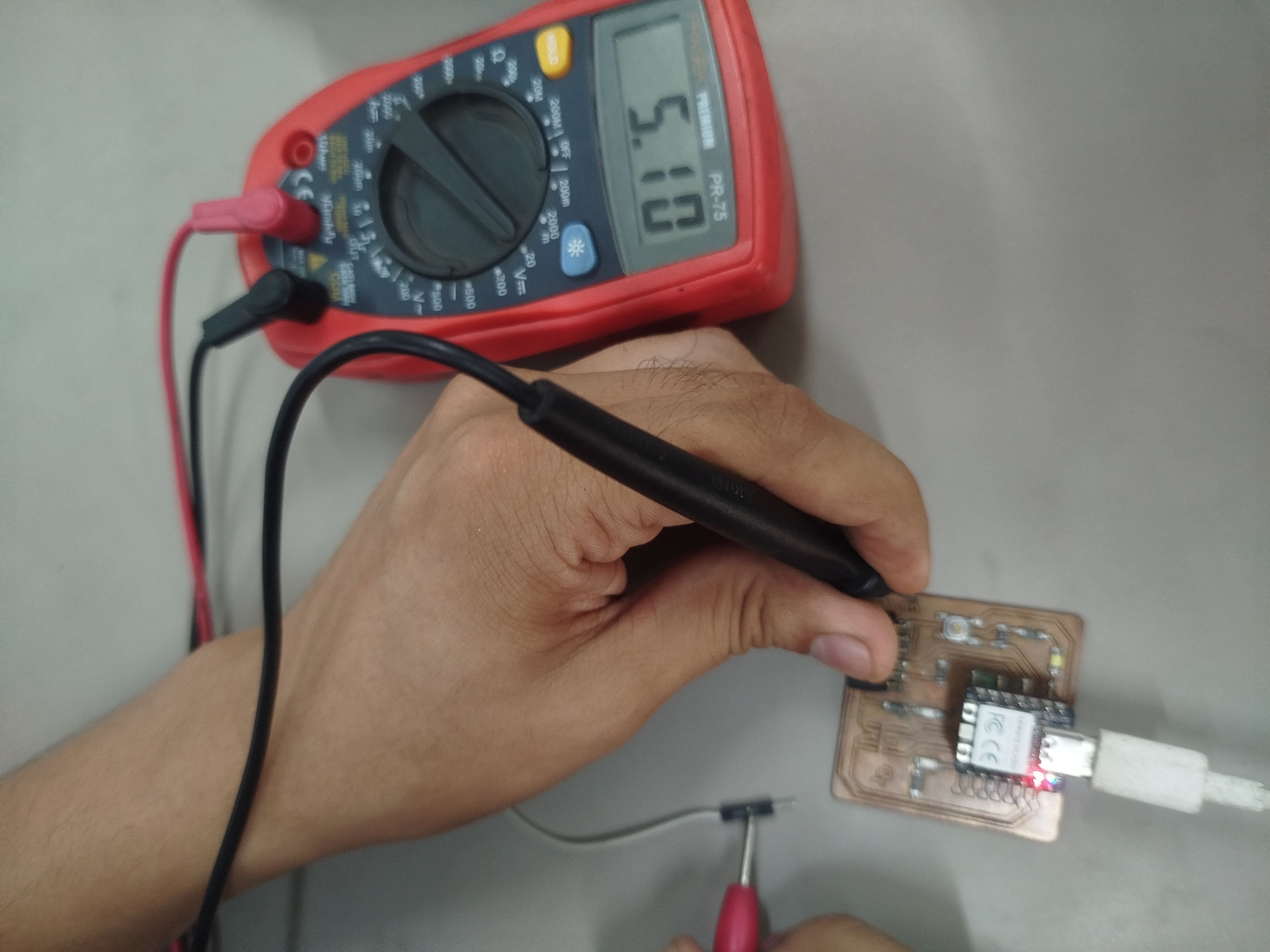
To verify the output voltages, we used a jumper wire and moved the multimeter knob to DC 20V, the output voltage being 5V correctly designed on the board.
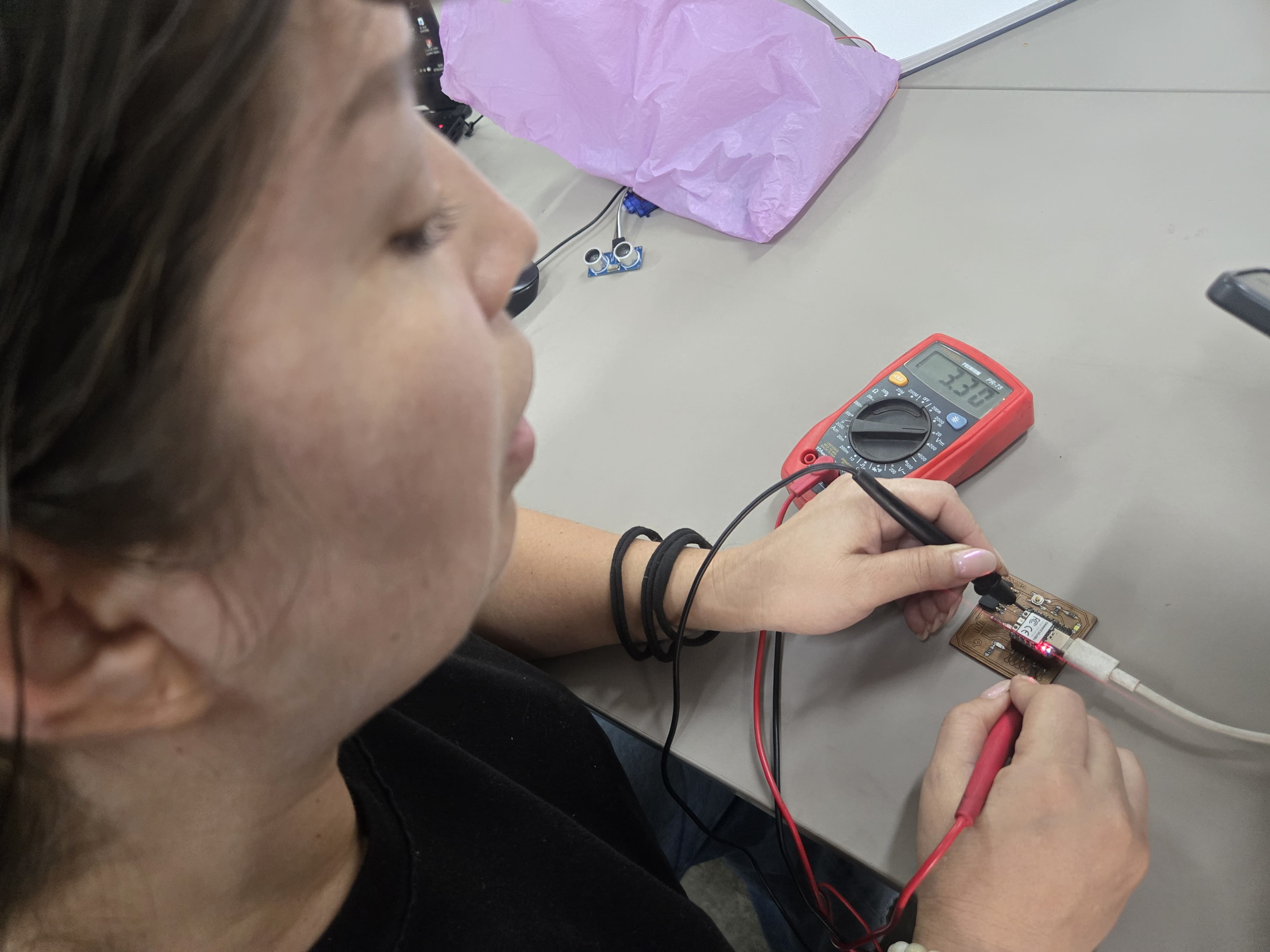
We also checked the 3.3V output of our microcontroller on the board to see if there was any voltage drop during soldering. To do this, we located the pin corresponding to the board's voltage.
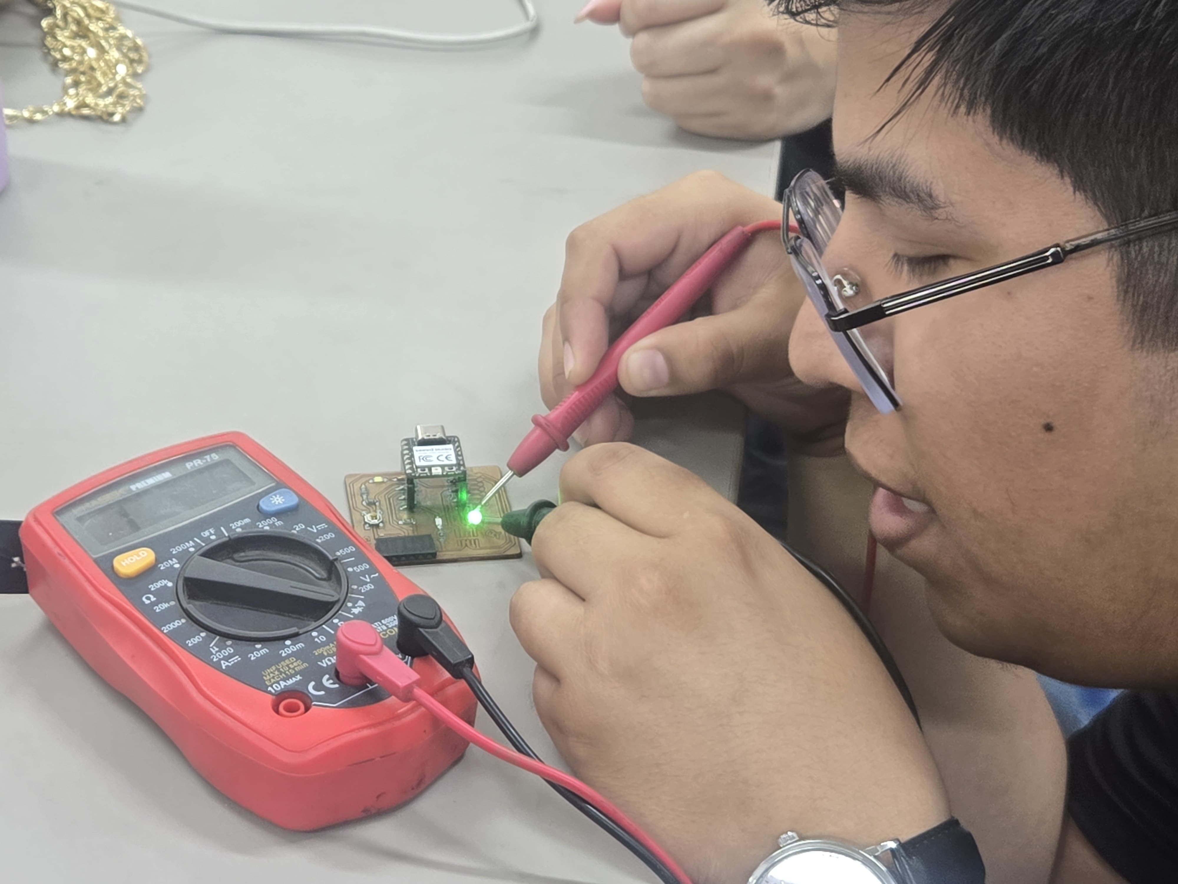
Finally, we check that our LED and SMD resistors are not damaged or burned out.
GW Instek GDS-1152A Digital Oscilloscope
Main features:
- Bandwidth: 150 MHz.
- 2 channels (CH1 and CH2).
- Color LCD screen.
- AutoSet Function.
- VOLTS/DIV and TIME/DIV adjustment.
- Internal memory for signal storage.
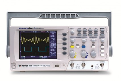
Use in group practice:
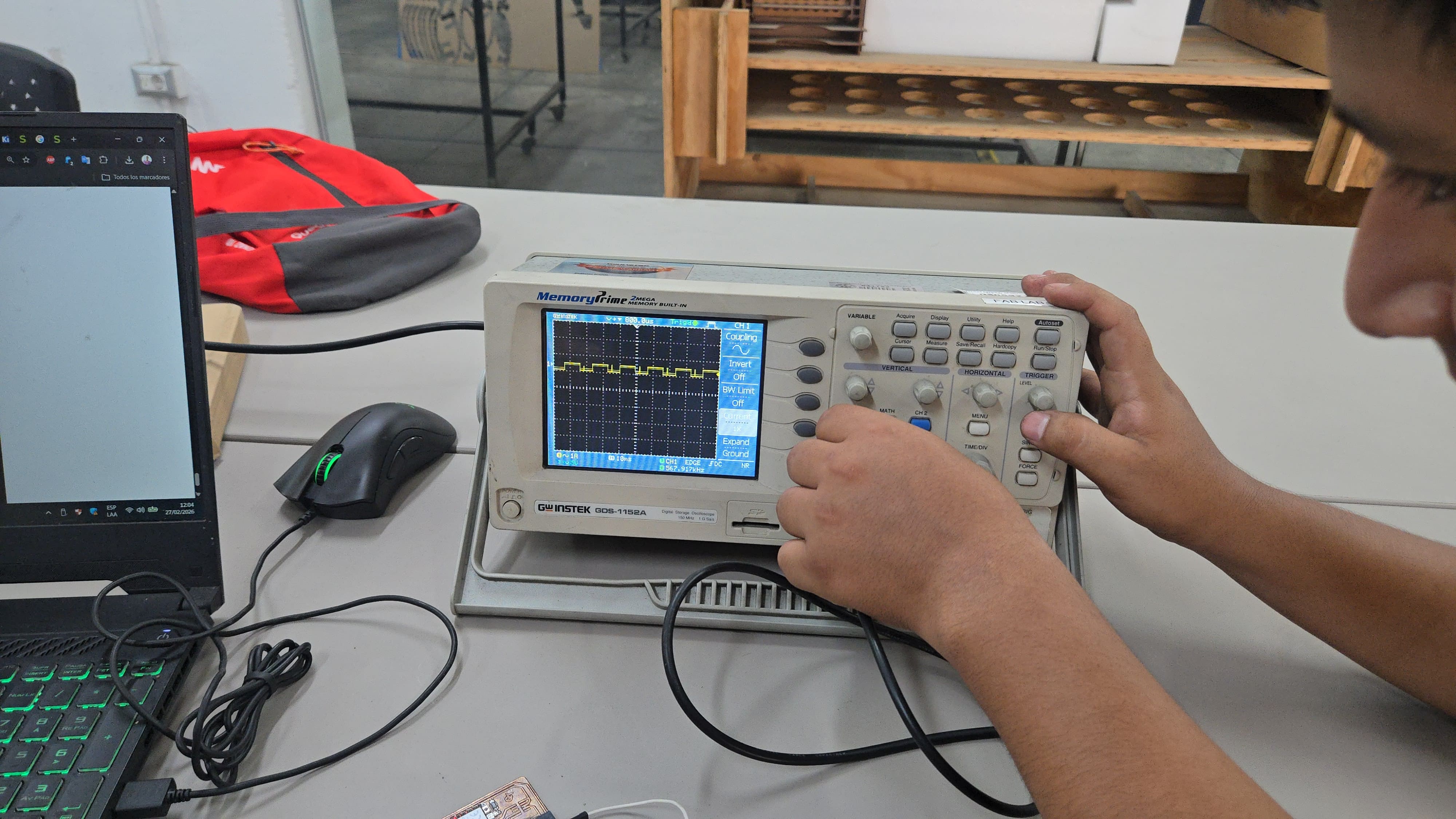
It was used to observe the digital signal generated by the RP2040 microcontroller, visualize the square waveform, measure voltage levels (0V – 3.3V) and analyze the temporal behavior of the signal.
We also use the GW Instek GDS-1152A oscilloscope, which is a two-channel digital oscilloscope.
This equipment is used to view signals over time (for example, a square wave or a PWM signal).
- Oscilloscope setup: ground clip (black) → board GND; probe tip → GPIO pin set as output.
- Configuration used: CH1 channel; voltage scale 1 V/div; time scale 1 ms/div; trigger Edge mode (CH1); Auto Set for initial calibration.
- After programming the RP2040 to generate a square wave, we observed a clear digital square signal.
- Voltage levels between 0 V and approximately 3.3 V.
- Stable frequency matching the programmed timing.
- This confirmed correct execution of the microcontroller, proper GPIO pin operation, and stable voltage regulation.
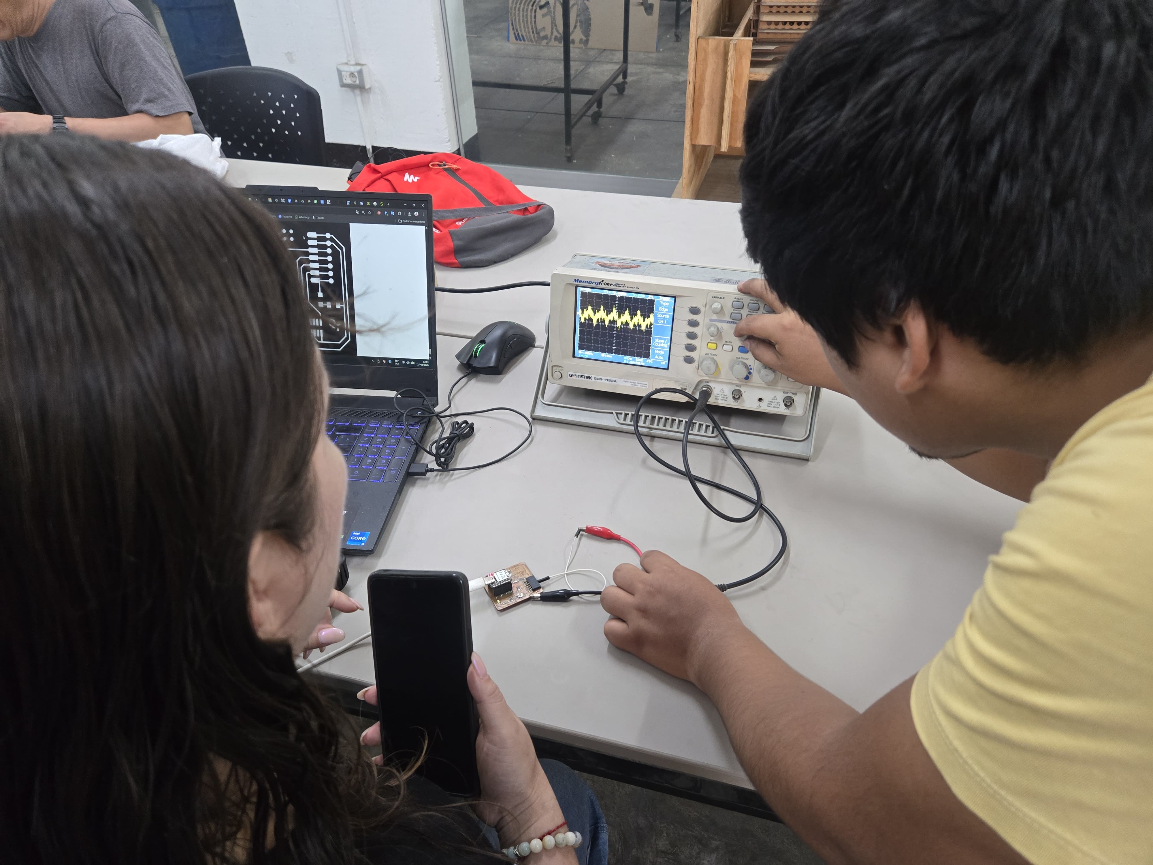
Results:
- The oscilloscope showed a clean square wave, which confirms that:
- The microcontroller's internal clock is operating correctly.
- The digital pin toggles between LOW and HIGH states properly.
- The board's power supply is stable.
What We Learned:
- How to properly connect an oscilloscope to an electronic board.
- The importance of connecting GND properly.
- The difference between measuring voltage with a multimeter and visualizing signals with an oscilloscope.
- How real digital signals are observed in hardware.
Individual assignment:
- Use an EDA tool to design a development board that uses parts from the inventory to interact and communicate with an embedded microcontroller.
We will install KiCad!
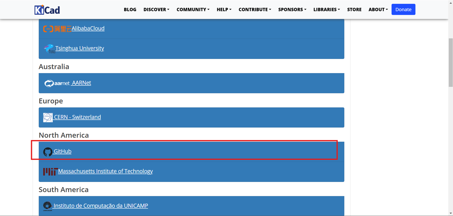
We will download the KiCad program for our PC and install it with the default options. You can download it here: KICAD
We will download the Windows version We will choose the GitHub option
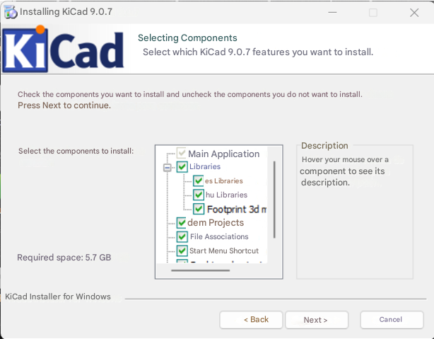
Click "Next" and we will install the default KiCad libraries.
Installing default libraries Ready to use
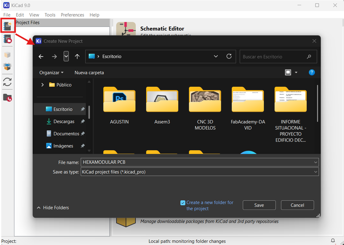
First, it is necessary to create a new project from scratch in a specific folder.
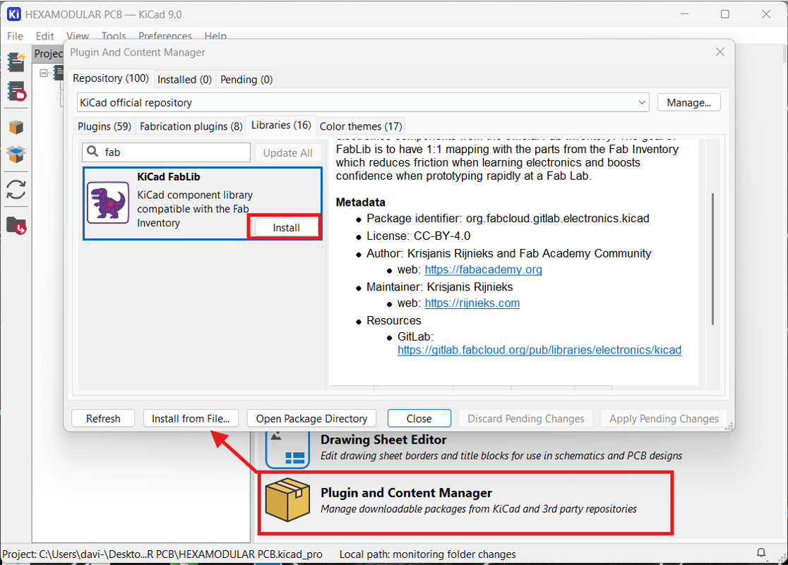
Next, click on "Plugin and content manager" to add the libraries needed for our design. In this case, we search for and add the KiCad FabLib library, then click install.
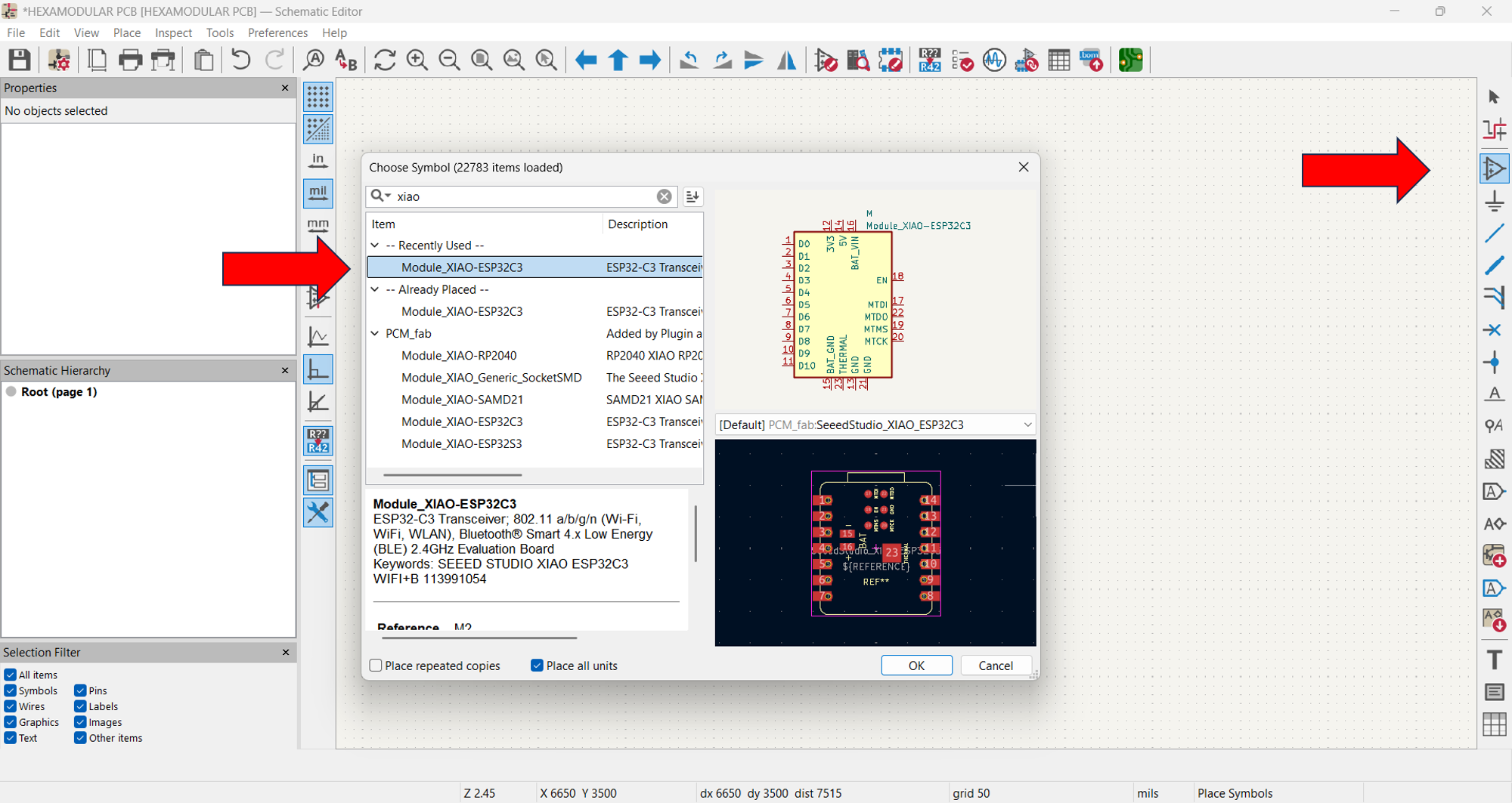
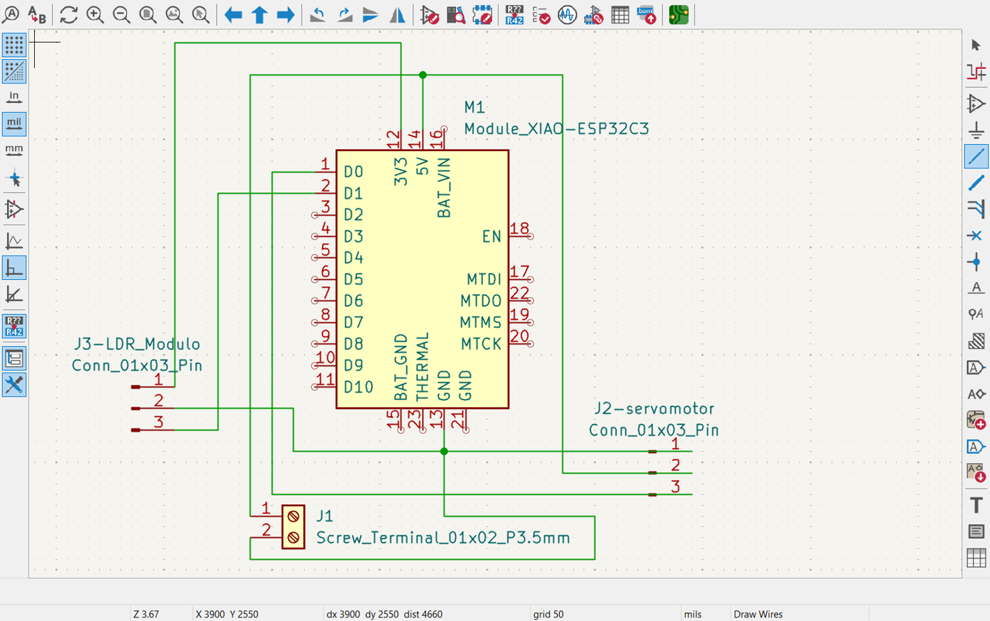
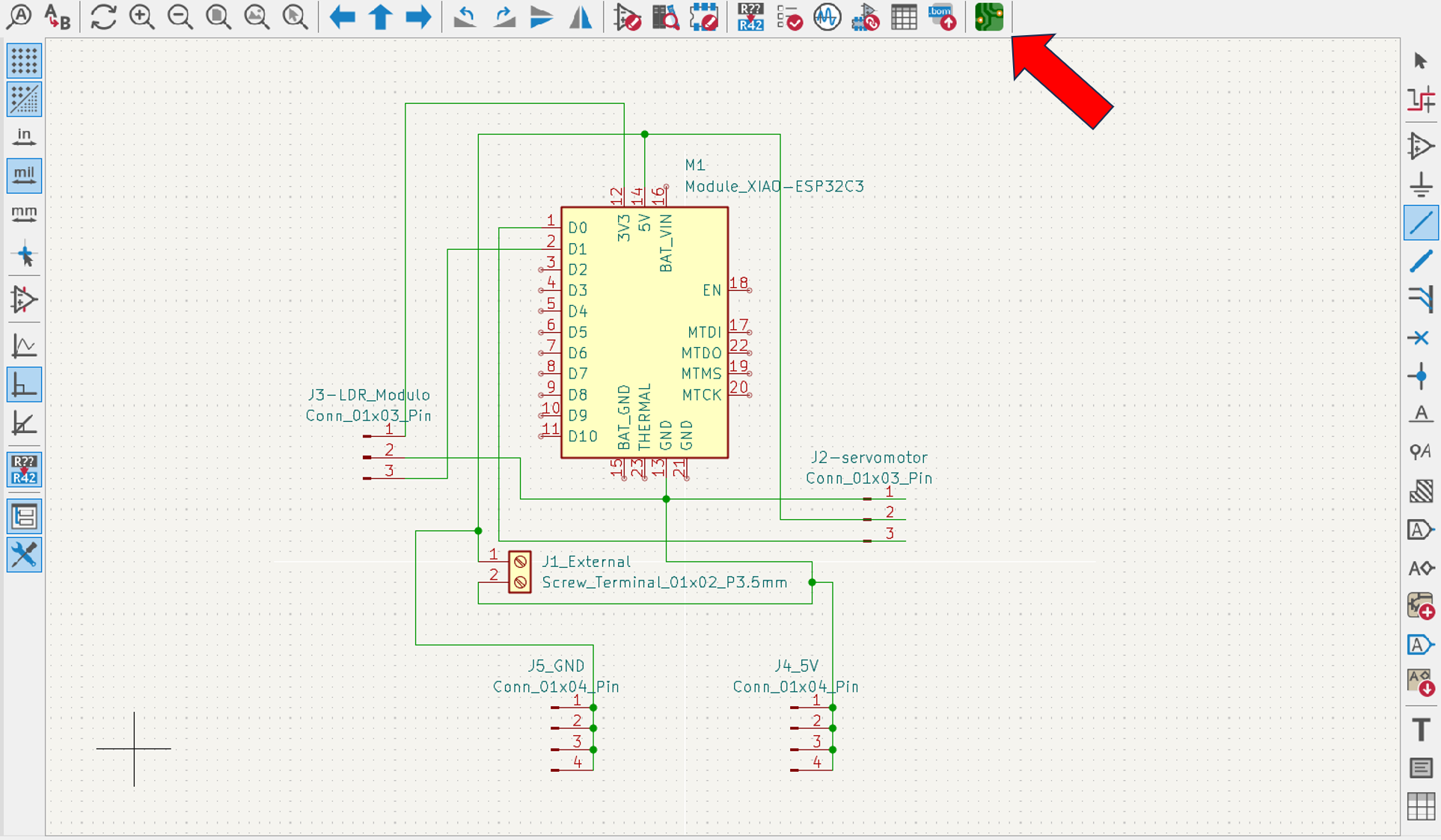
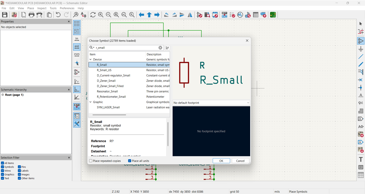
Click on "place symbols" and search for the XIAO ESP32C3 microcontroller, adding it to the schematic; in the same way, add more components.
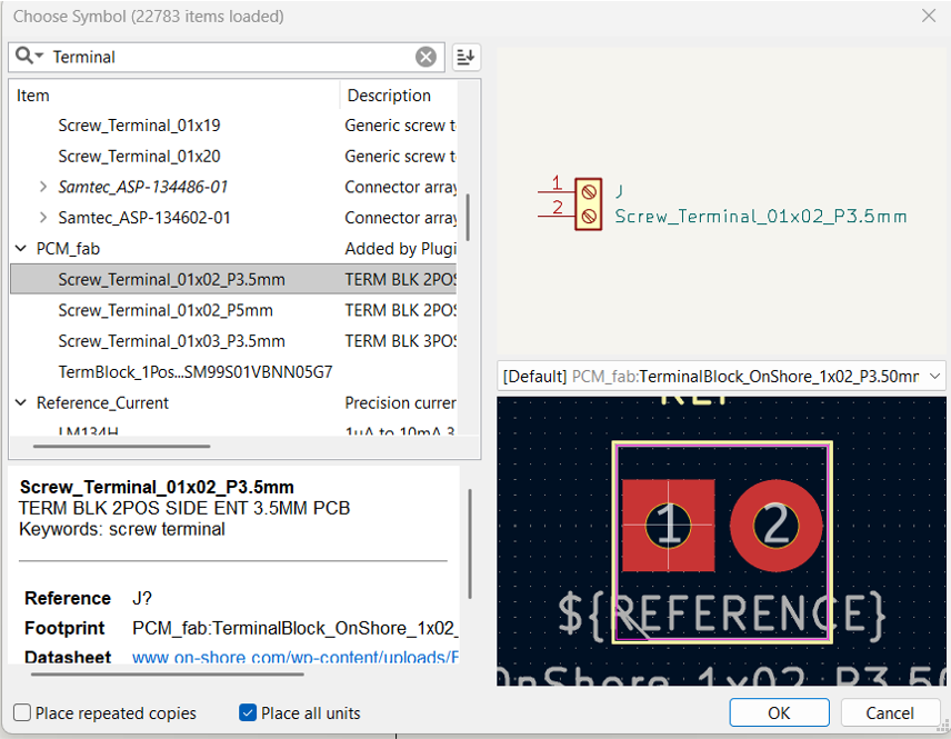
Now we add the terminal block for external power input; in this case it already has a footprint, as shown in the box below.
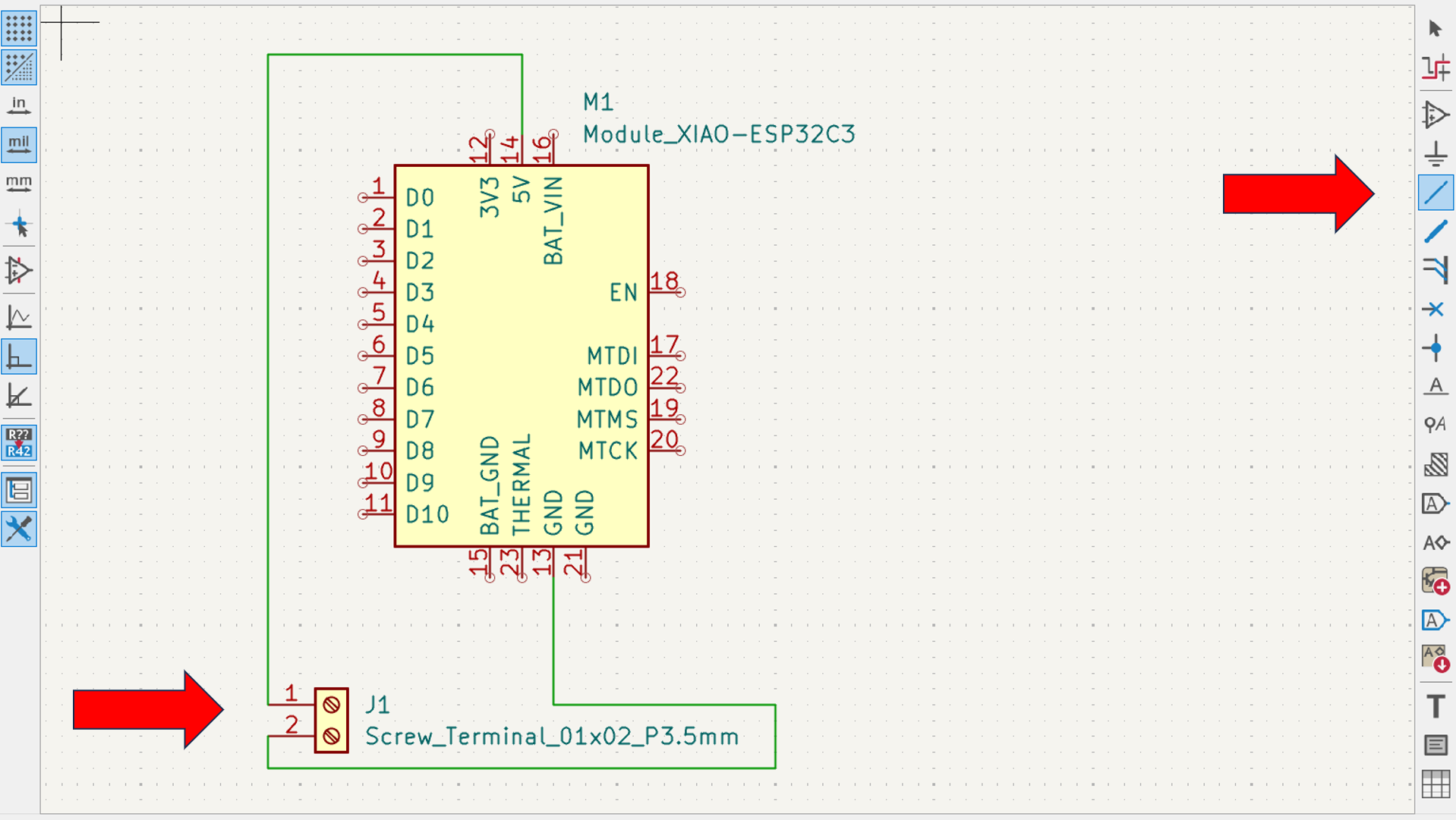
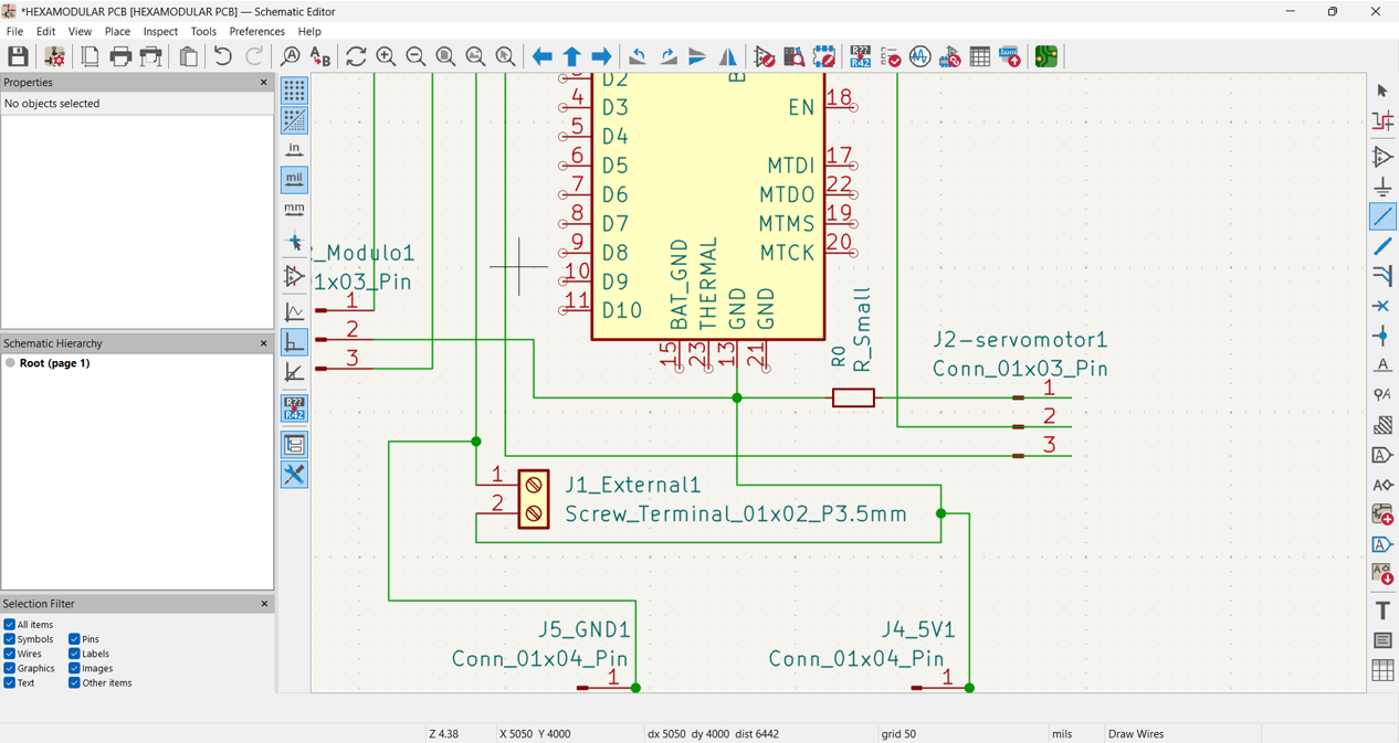
Then we proceed to connect the components following the microcontroller datasheet and the XIAO ESP32C3 reference board schematic; for this we use the Draw Wires command.
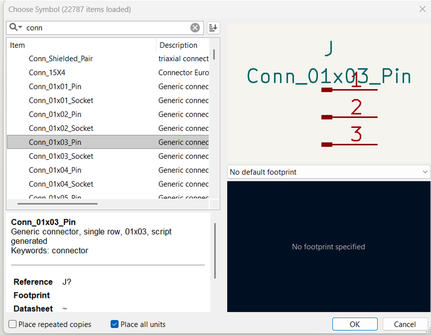
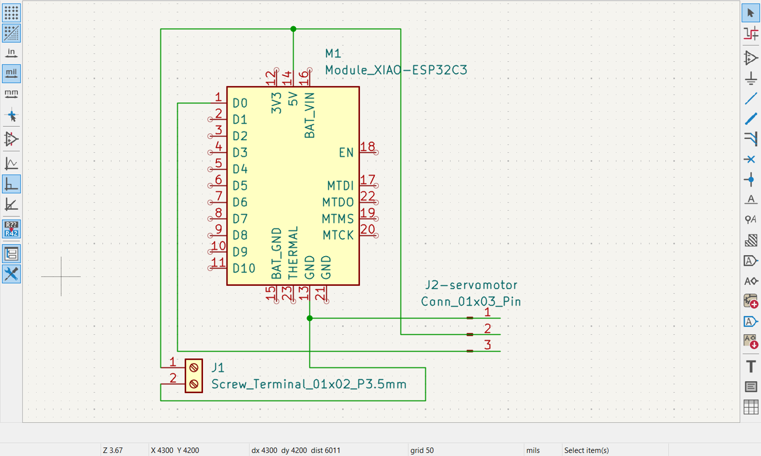
Next, we insert the output for our servo motor.
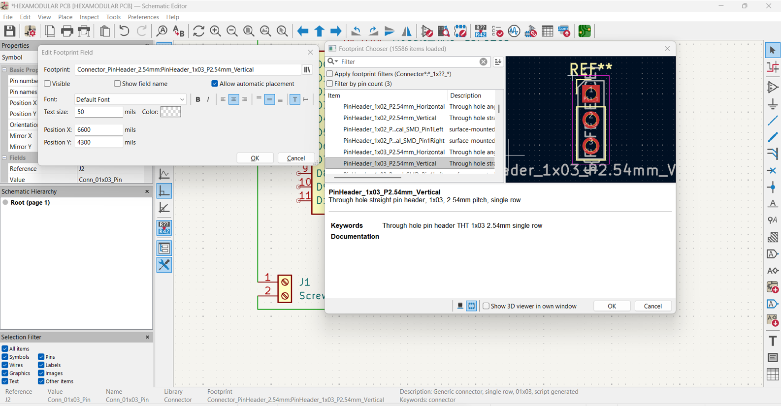
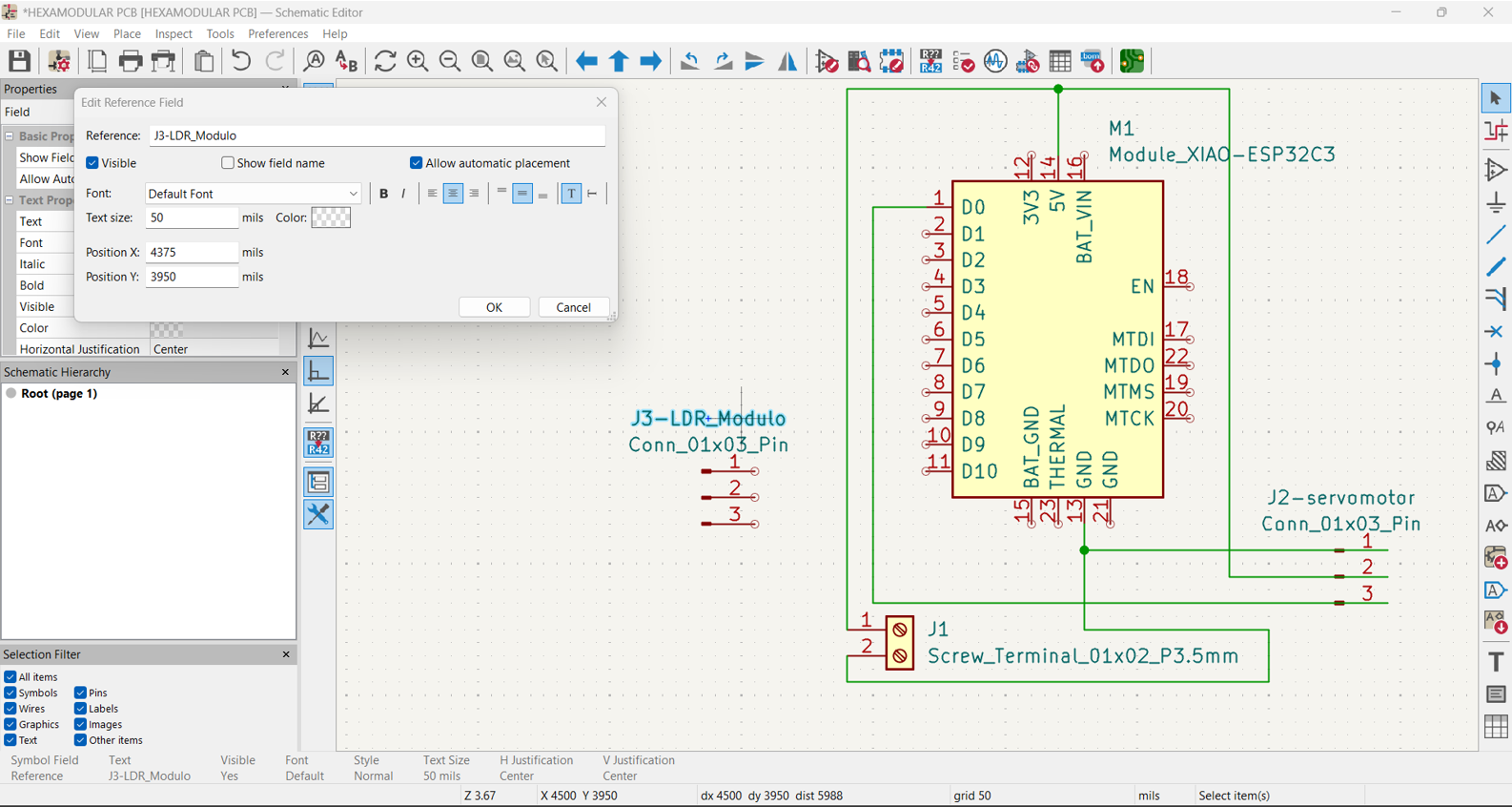
In this case, this library has no footprint, so we assign a reference by clicking the component and then pressing the (F) key. Then we continue with the connections to the XIAO.
We select the footprint We connect the components
We follow the same process to add our LDR module, assign its footprint, and then connect it.
Adding footprint Connecting components
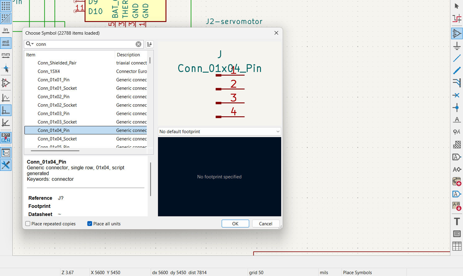
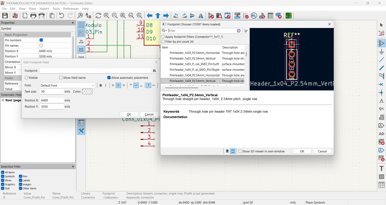
Finally, we add four 5V output pins and four GND pins. This allows us to connect other hexagonal modules in parallel. We assign the footprint and connect them while organizing expansions.
Adding footprint Connecting pins
This is how the schematic connections turned out according to the microcontroller datasheet and the XIAO ESP32C3 reference board schematic, with the corresponding footprint for each component.
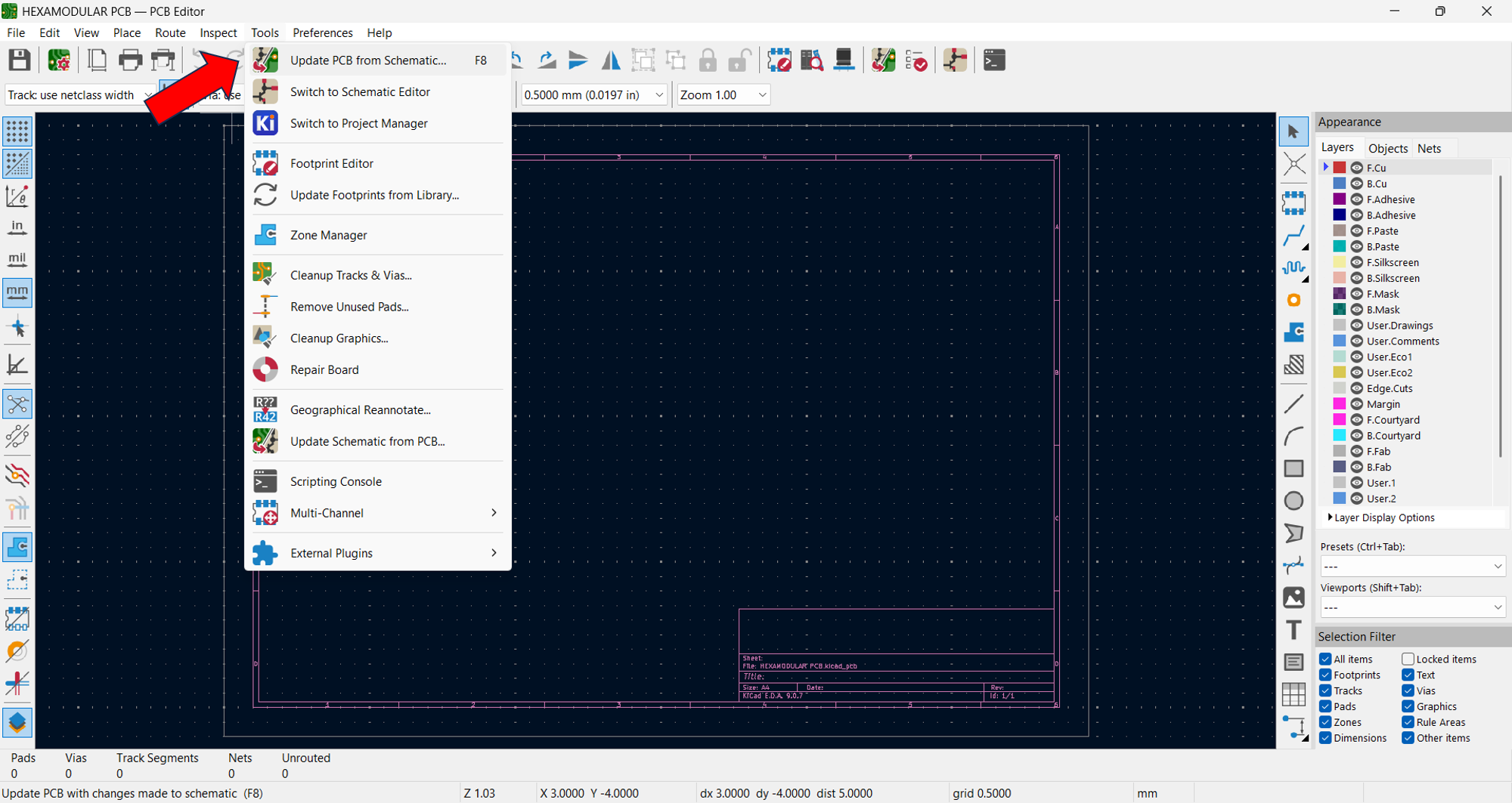
Then we move to PCB design by clicking the "Switch to PCB editor" icon.
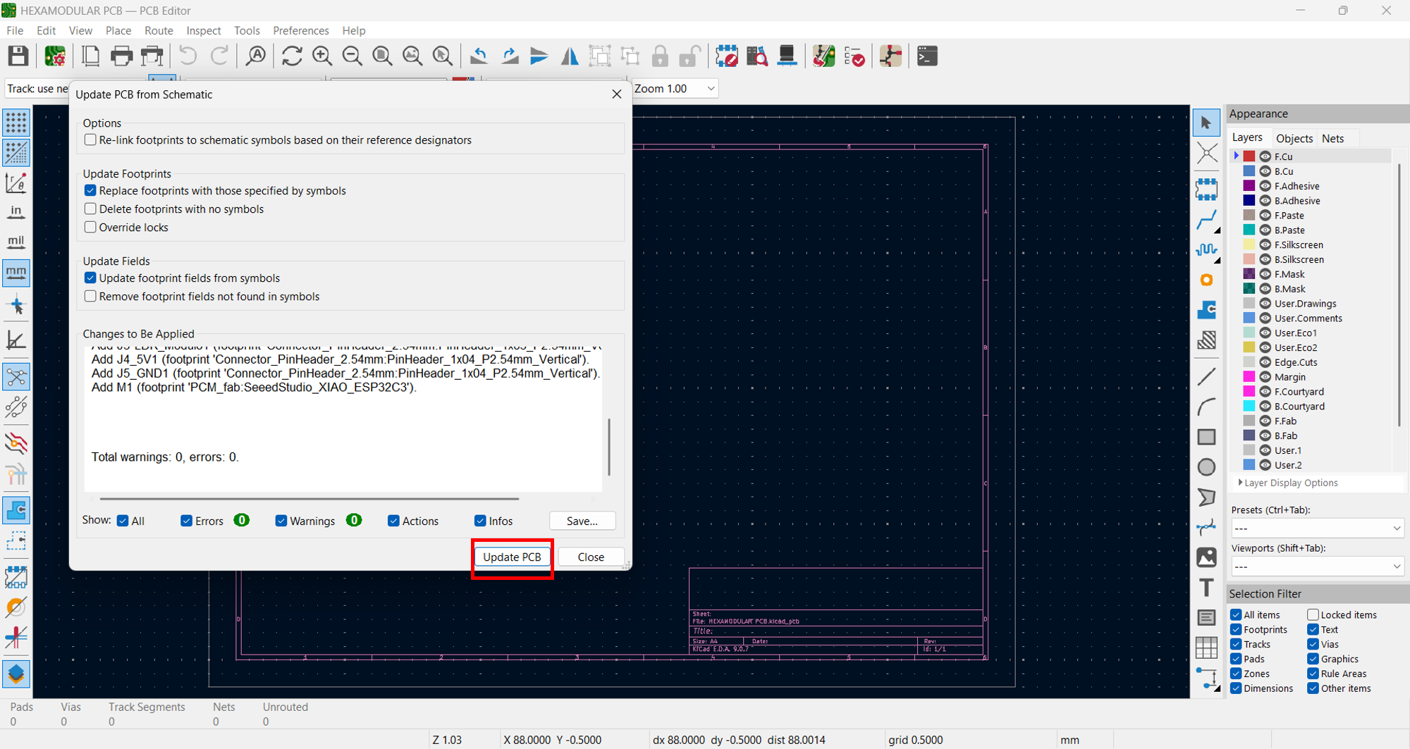
Click on "Tools" and then on "Update PCB from Schematic"; a dialog box appears where we click "Update PCB".
Open tools and choose update Apply changes from schematic
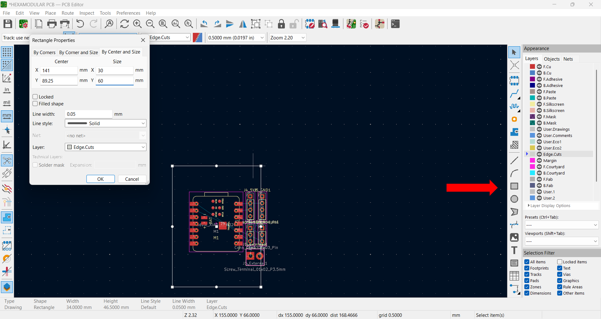
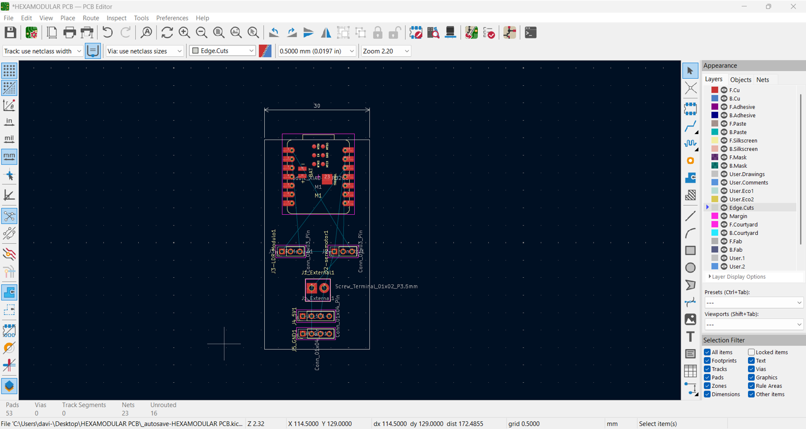
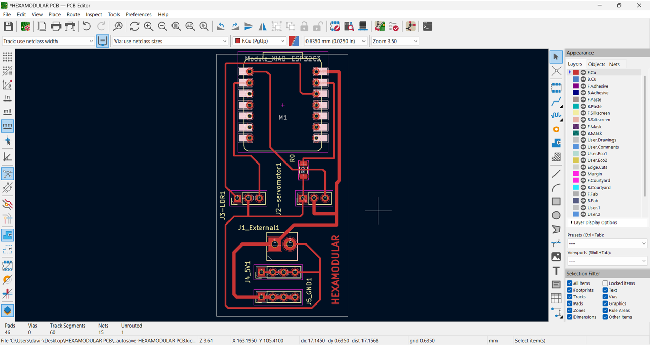
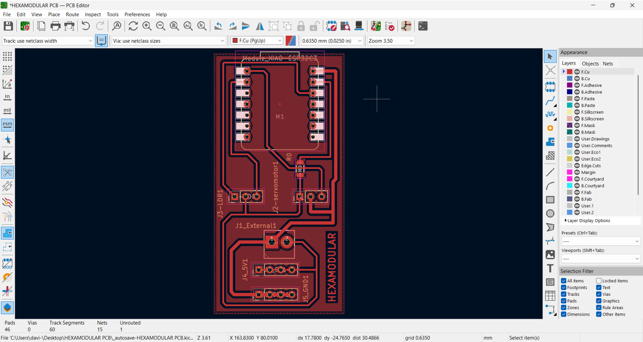
We draw a rectangle to define the board size, in this case 30 mm x 60 mm, and then arrange the connections within this rectangle to optimize space and avoid unnecessary crossings (we do this on the Edge.Cuts layer).
Define board dimensions Organize traces and parts
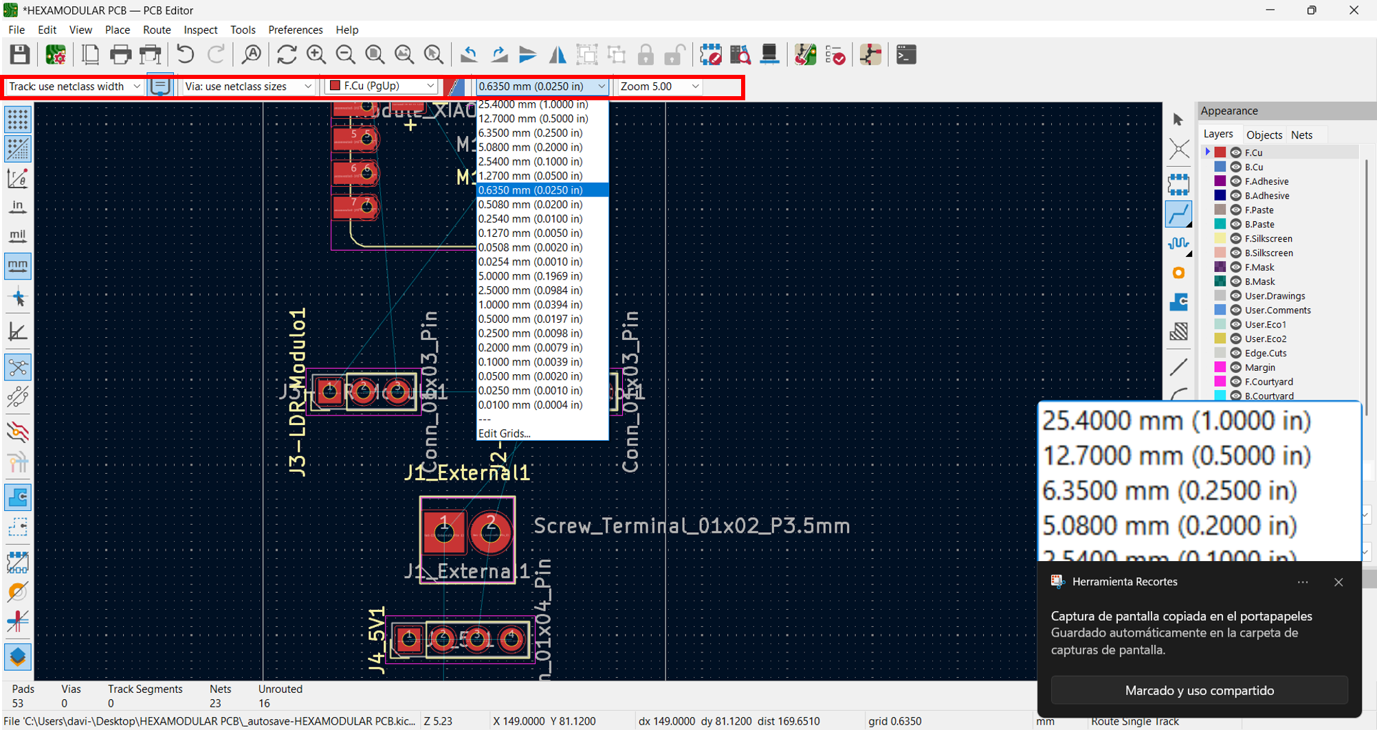
In this case, we will choose two track widths: 0.8 mm for 5V and 0.4 mm for the others.
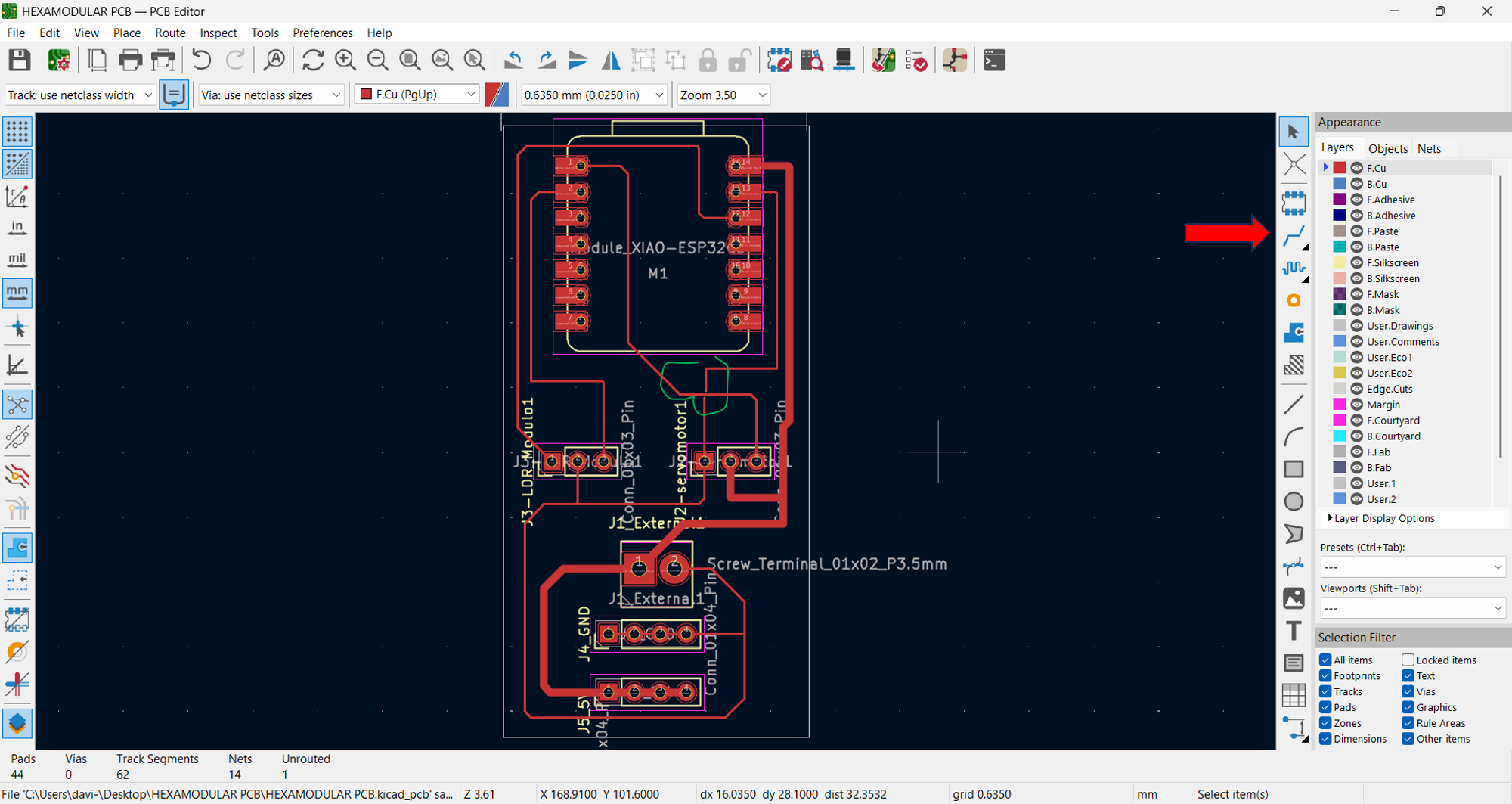
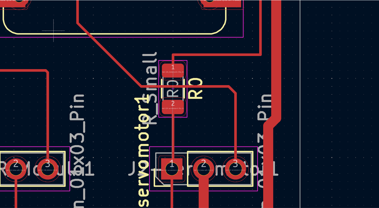
The track routing is done with the "Route Tracks" command, connecting the components according to the schematic while optimizing space and avoiding unnecessary crossings. The layout turned out like this, with one note: we need to make a bridge at the GND pin between the servo and the XIAO.
We insert a 0Ω SMD resistor to create a bridge on the missing track. For that, we return to the schematic, insert it, and make a new connection including the resistor in the path.
Insert in schematic Connection completed
Then we switch to PCB design, update it, and route the track as well. In this case, we rotate the SMD with the R key for the correct alignment with the track junction.
The connections turned out as shown in the image; from there, I only cleaned up some text labels and edited the XIAO library.
I also added the name of my board: "HEXAMODULAR".
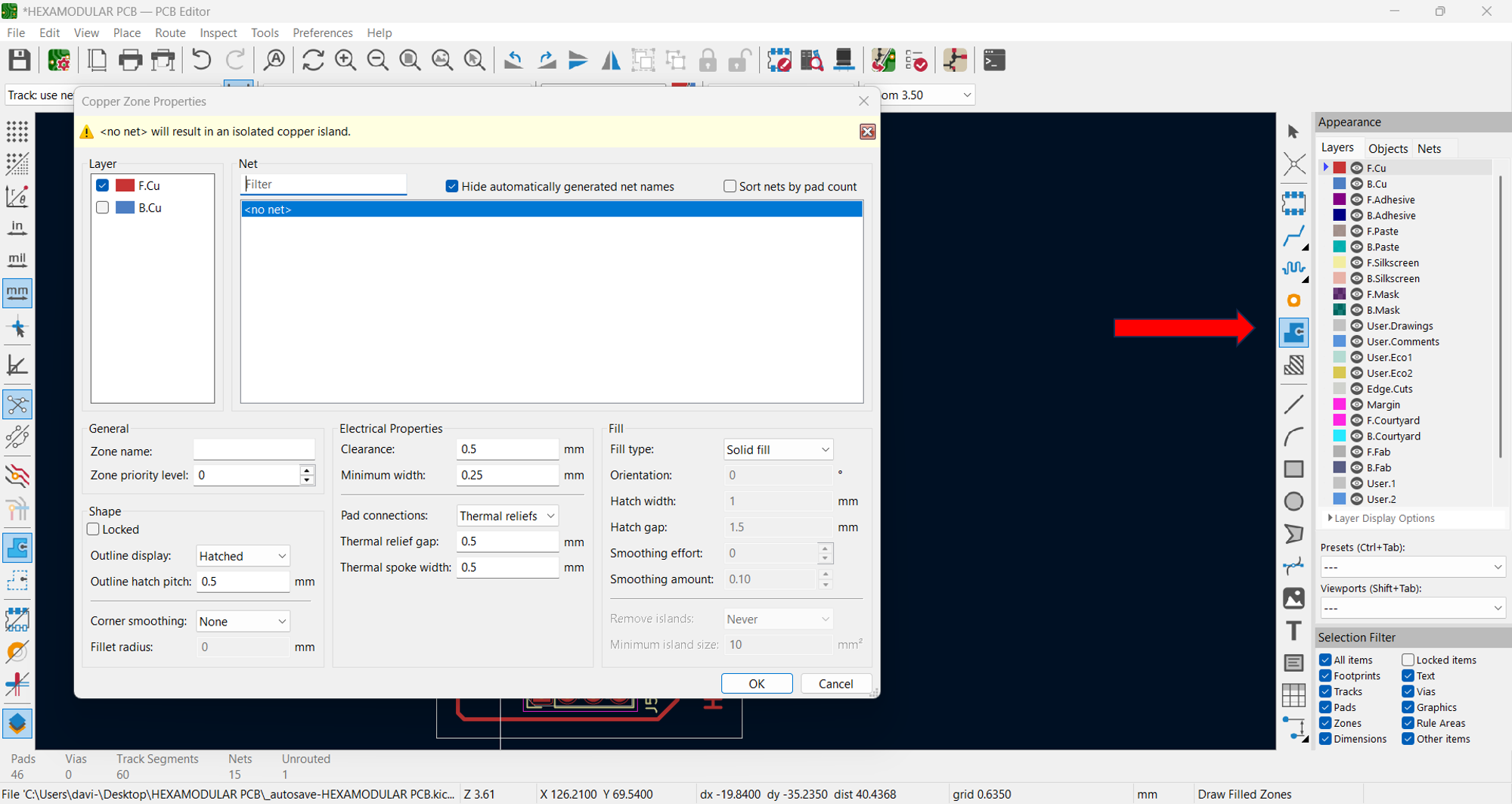
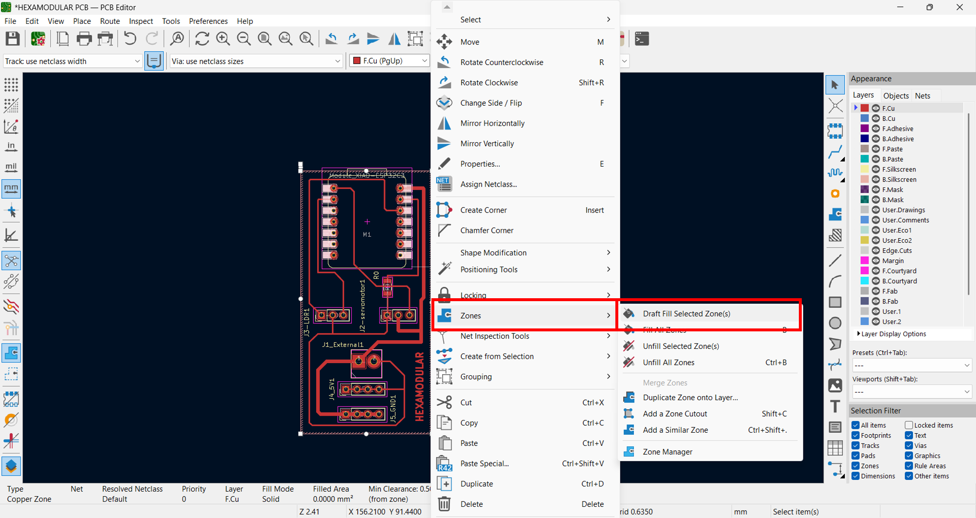
Click on "Draw Filled Zones" to create a copper zone, select the default values, and draw the zone around the whole board. This helps provide a better GND reference and avoid signal noise issues.
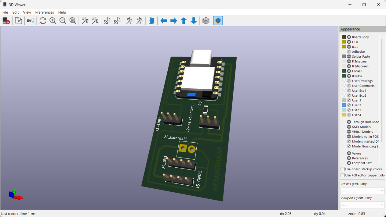
After that, right-click the zone and select "Draft Filled Zones" to update the zone and display copper in the design. This is how the final design of my hexagonal development board with the XIAO ESP32C3 microcontroller and its corresponding connections turned out.
This is how the design looks with the copper zone highlighted.
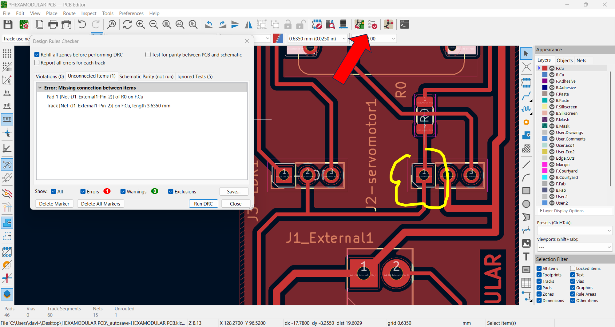
We run the "DRC" check to verify there are no design errors, and then export the Gerber files for board fabrication. I found a default warning because KiCad recognizes two different track types that end very close to each other, but this can be ignored or solved by adding a copper-filled pad since it can be treated as a continuous trace.
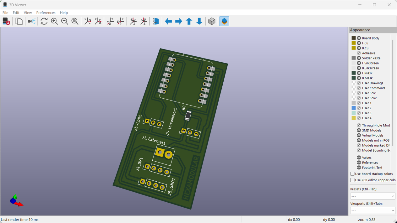
3D VIEW WITHOUT COMPONENTS
3D VIEW WITH COMPONENTS. THIS IS THE FINAL DESIGN OF MY HEXAGONAL DEVELOPMENT BOARD WITH THE XIAO ESP32C3 MICROCONTROLLER AND ITS CORRESPONDING CONNECTIONS.
Conclusions:


Libraries Setup
Libraries Installed
Servo Motor
Servo Motor
LDR Module
LDR Module
5V Output Pins
5V Output Pins
PCB Update
PCB Update
Board Outline
Component Layout
0Ω Resistor
Track Bridge
FILES