Assignment Requirements
Group assignment
- Measure the power consumption of an output device.
- Document your work on the group work page and reflect on your individual page what you learned.
Individual assignment
- Add an output device to a microcontroller board you've designed and program it to do something.
Progress Status
This is for reporting progress (not for visitors to click).
Group page link + notes added.
Missing final photos and conclusions.
Upload .zip with source files.
Assignment Requirements
Learning outcomes
- Demonstrate workflows used in controlling an output device(s) with MCU board you have designed.
Have you answered these questions?
- Linked to the group assignment page.✅
- Documented how you determined power consumption of an output device with your group.✅.
- Documented what you learned from interfacing output device(s) to microcontroller and controlling the device(s).✅.
- Linked to the board you made in a previous assignment or documented your design and fabrication process if you made a new board.✅.
- Explained how your code works.✅.
- Explained any problems you encountered and how you fixed them.✅.
- Included original source code and any new design files.✅.
- Included a ‘hero shot’ of your board.✅.
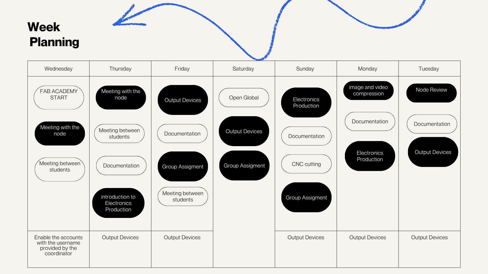
Weekly planning
During the week, we carried out various activities that presented significant challenges but were also very rewarding, especially due to the opportunity to share and learn as a team. We met virtually with our colleagues at the node and participated in lab meetings, which allowed us to organize ourselves and conduct open workshops in different spaces. In these sessions, we reviewed and worked with input devices, understanding their operation and their importance in capturing data from the environment for subsequent processing in electronic systems.
group work
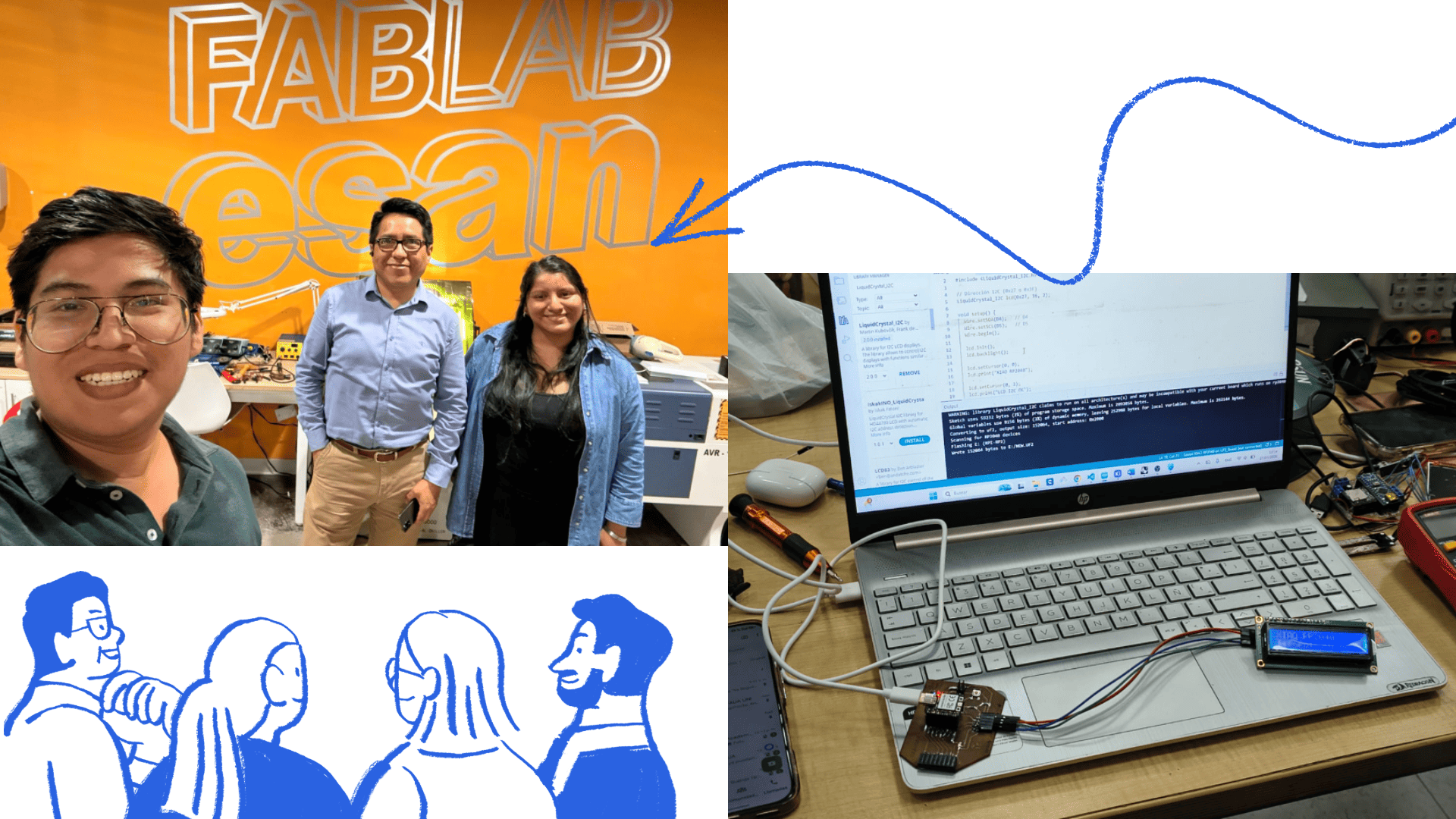
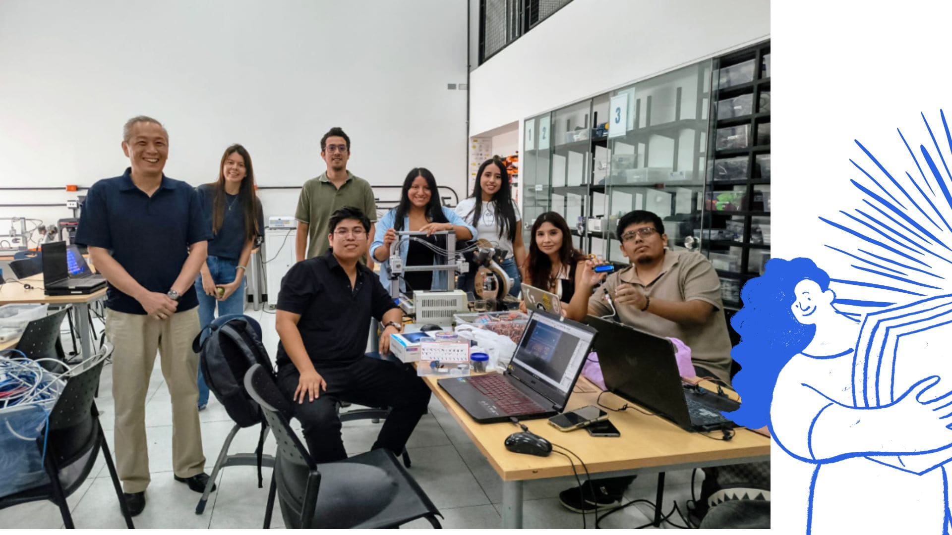
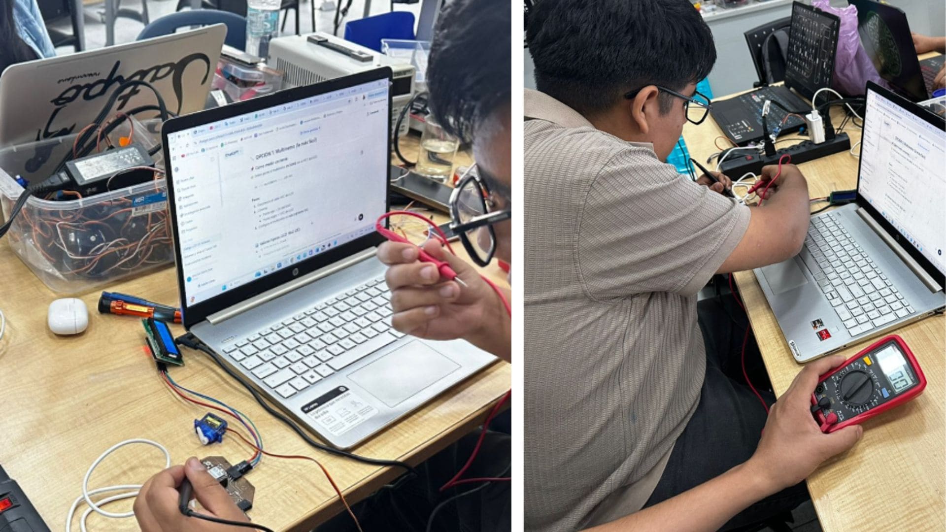
This week, focused on Input Devices, we held an in-person meeting at the Fab Lab UNI node. Colleagues in other cities also participated virtually, allowing the entire group to connect. In this stage, we worked with input devices, which capture information from the environment (such as light, temperature, or pressure) and transform it into signals that can be interpreted by electronic systems. We used various sensors and measuring tools for this purpose. During the practical sessions, we used equipment such as the oscilloscope and the multimeter, which helped us analyze electrical signals, verify voltages, and ensure the correct functioning of the circuits. These tools were essential for understanding how the sensors interact with the motherboard and how the data obtained is processed.
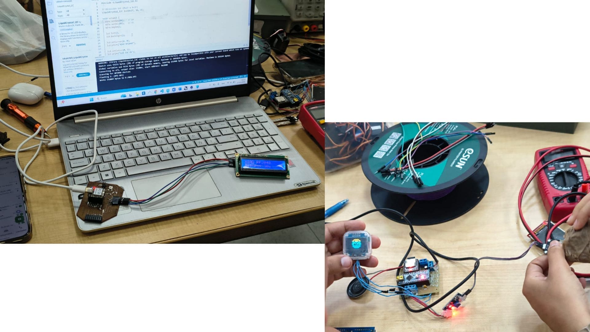
In this group project, I learned to find and integrate the necessary libraries for each of the output devices used, subsequently verifying that the code compilation was correct. For this exercise, we worked with the FABXIAO board developed by Adrian Torres, using an LCD screen as the first device.
Verification of Device Power Consumption
Initially, we developed the code to control both the LCD screen and the servomotor. Then, we connected the components to the board and proceeded to measure power consumption using a multimeter. Power consumption was evaluated both at rest and during operation of each device.
Subsequently, we verified the results by applying the basic formula for electrical power, which allowed us to validate the measurements obtained. In conclusion, it was confirmed that the servomotor has a higher power consumption compared to the LCD screen, which is consistent with its electromechanical nature and movement requirements.
Tools and Components Used
- Adrian Torres microcontroller board
- Seeed Studio XIAO RP2040
- HC-SR04 ultrasonic distance sensor
- servomotor
- LCD screen
This experience allowed us to better understand how input devices capture and transmit data, as well as how signals can be measured and interpreted using laboratory equipment.
Procedures: Output Devices Analysis
You can view the complete group work here: View Group Project
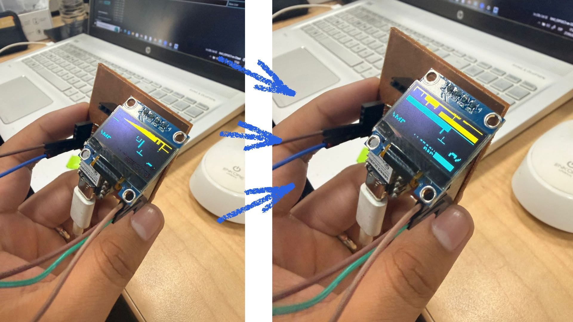
Procedure: OLED Display + Joystick Control (ESP32-C3 PCB)
1. Description
A control system was implemented on a PCB using the ESP32-C3 microcontroller, integrating a joystick and an OLED display. The joystick provides analog input for X and Y axis movement, while the OLED screen displays real-time graphical information.
- Joystick: Analog input (A0, A1) + button (D2)
- OLED: I2C communication (SDA, SCL)
- Function: Real-time interaction and graphical display
- Application: Snake game and dynamic interface
This implementation is important to validate proper integration between input devices and display systems in an embedded PCB design.
2. Hardware and Software Setup
- ESP32-C3 microcontroller (PCB)
- Joystick connected to A0, A1, D2
- OLED display connected via SDA and SCL (I2C)
- Pull-up resistors for I2C communication
Programmed using Arduino IDE, including graphics and communication libraries for OLED control.
3. Signal Observation
After programming, real-time interaction between the joystick and the OLED display was observed, confirming:
- Correct reading of analog signals from the joystick
- Stable I2C communication with the OLED display
- Proper graphical updates on the screen
- Fluid control in the Snake game interface
4. Reflection
During the development process, special attention was required for library configuration and system setup, as some errors required reinstallation and verification. Additionally, it was necessary to optimize I2C communication and adjust joystick thresholds to avoid unstable readings. Despite these challenges, the system achieved smooth interaction, demonstrating the capability of the PCB for more advanced embedded applications.
Conclusions
Through this individual contribution to the group assignment, I was able to better understand the importance of measuring and analyzing electronic signals using laboratory tools such as the multimeter and oscilloscope. This experience helped me reinforce my knowledge about input devices, sensor behavior, and real-time data acquisition.
I also learned the importance of correct circuit configuration, proper library installation, and stable communication between components such as the OLED display and sensors. After solving connection and configuration issues, stable readings and correct system interaction were successfully achieved.
Finally, this activity allowed me to better understand how electronic systems process environmental information and how these concepts can later be integrated into my final project and the mobile laboratory proposal.
group assignment
Individual Assignment – Input and Output Devices Programming
The main objective of this individual assignment was to integrate both input and output devices capable of capturing environmental information and displaying it in real time through a microcontroller system.
For the input stage, sensors such as the DHT11 and the LDR sensor were implemented to measure environmental variables including temperature, humidity, and light intensity. The collected data was processed using the XIAO ESP32-C3 microcontroller.
For the output stage, an OLED SSD1306 display was incorporated as the main output device, allowing real-time visualization of the sensor readings. This integration demonstrated how environmental data can be captured, processed, and immediately displayed to the user.
Additionally, the electronic production board previously designed during the Electronics Production assignment was reused, maintaining continuity with the final project proposal and the concept of the mobile laboratory. This allowed the integration of previous knowledge with the current assignment focused on input and output devices.
The assignment also reinforced the relationship between hardware and programming by combining sensors, display systems, and embedded programming into a functional environmental monitoring prototype.
Programming
The system was programmed using the Arduino IDE development environment. Several libraries were installed to enable communication between the sensors, the OLED display, and the XIAO ESP32-C3 microcontroller.
To ensure proper operation of the DHT11 sensor, the DHT.h library developed by Adafruit was installed through the Library Manager.
Similarly, libraries such as Wire.h, Adafruit_GFX.h, and Adafruit_SSD1306.h were used to establish communication with the OLED display using the I2C protocol.
The program continuously reads temperature, humidity, and light intensity values. The information is processed by the microcontroller and then displayed both on the OLED screen and the Serial Monitor for validation purposes.
Components Used
| Component | Function |
|---|---|
| XIAO ESP32-C3 | Main microcontroller and data processing unit |
| DHT11 | Temperature and humidity input sensor |
| LDR Sensor | Light intensity input sensor |
| OLED SSD1306 | Output device for real-time data visualization |
| Resistors | Electrical stability and voltage division |
| Jumper Wires | Connections between components |
| USB-C Cable | Power supply and programming connection |
Component Connections
DHT11 Sensor (Input Device)
The DHT11 sensor was used as an input device to capture environmental temperature and humidity data.
| DHT11 Pin | Connection |
|---|---|
| VCC | 3.3V |
| GND | GND |
| DATA | GPIO 21 |
The sensor sends digital environmental data directly to the XIAO ESP32-C3 for processing.
LDR Sensor (Input Device)
The LDR sensor was implemented to detect changes in ambient light intensity through analog readings.
| LDR Pin | Connection |
|---|---|
| One side | 3.3V |
| Other side | ESP32-C3 Analog Pin |
| Resistor | GND |
The microcontroller uses the analogRead() function to interpret variations in light intensity detected by the LDR sensor.
OLED SSD1306 Display (Output Device)
The OLED SSD1306 display was incorporated as the main output device of the system. Its purpose was to visualize environmental data in real time, improving interaction between the user and the monitoring system.
| OLED Pin | Connection |
|---|---|
| VCC | 3.3V |
| GND | GND |
| SDA | ESP32-C3 SDA |
| SCL | ESP32-C3 SCL |
Communication between the OLED display and the microcontroller was established using the I2C communication protocol.
General System Operation
- The DHT11 sensor measures environmental temperature and humidity.
- The LDR sensor detects ambient light intensity.
- The XIAO ESP32-C3 processes the sensor data.
- The OLED display visualizes the information in real time.
- The Serial Monitor validates the readings during operation.
Output Device Functionality
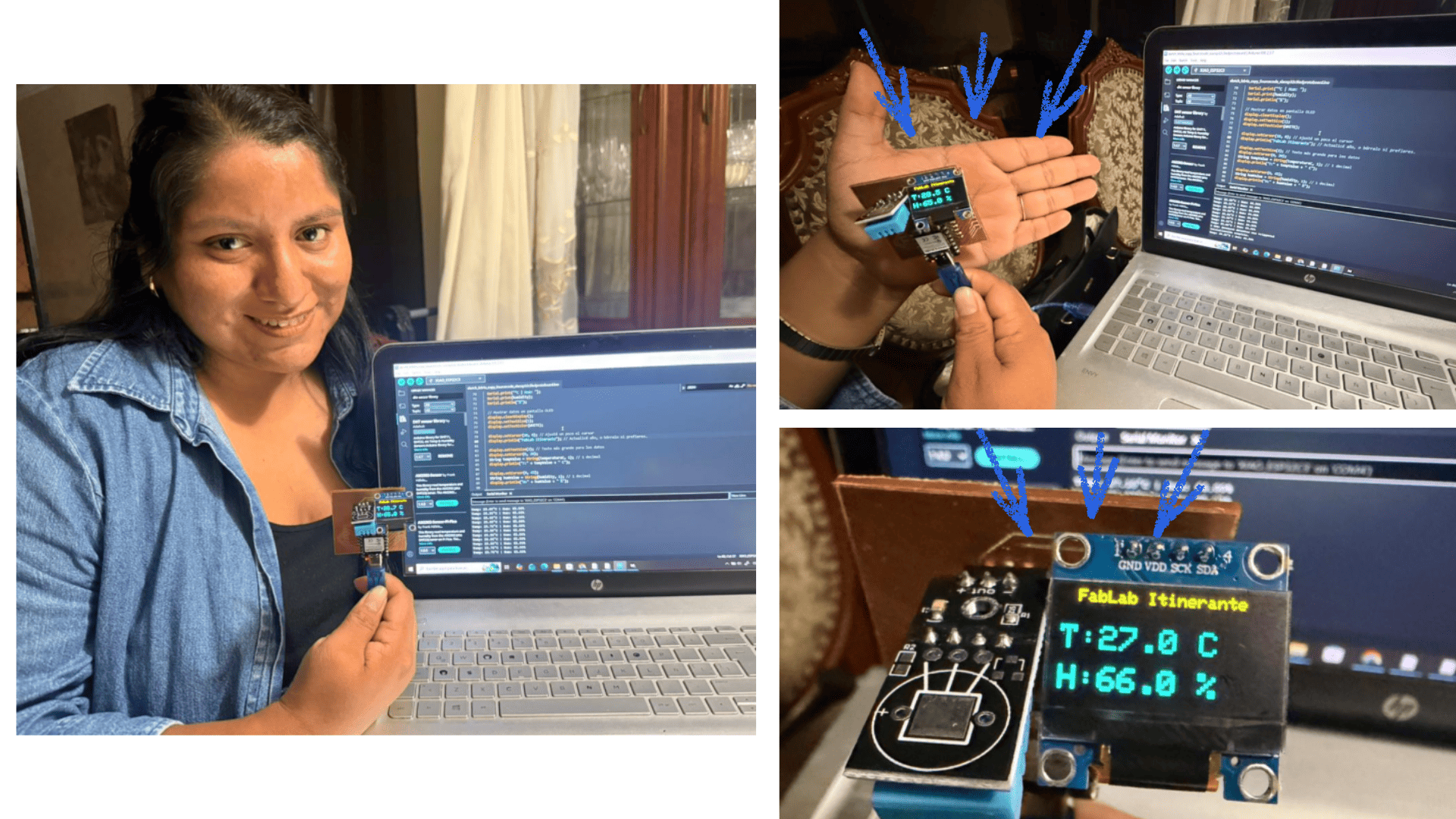
The OLED display plays an important role as the output device of the system. It provides immediate visual feedback by displaying environmental information directly on the screen.
The screen updates every two seconds, showing temperature, humidity, and light values in a clear and organized format. This allows users to monitor environmental conditions without requiring a computer connection once the system is powered.
The integration of the OLED display demonstrates how output devices can transform sensor data into accessible visual information for real-time interaction and monitoring.
System Validation
The complete system was tested to validate communication between the XIAO ESP32-C3, the environmental sensors, and the OLED output device.
During testing:
- The Serial Monitor displayed stable sensor readings.
- The OLED display correctly visualized the data in real time.
- The environmental information updated every two seconds.
- The system maintained stable communication between all components.
Serial Monitor Output
Initialization complete.
Temp: 27.4 C | Hum: 74.0%
Temp: 27.5 C | Hum: 73.0%
Temp: 27.6 C | Hum: 74.0%
These tests validated the correct operation of both the input and output devices, confirming the stability and reliability of the environmental monitoring system.
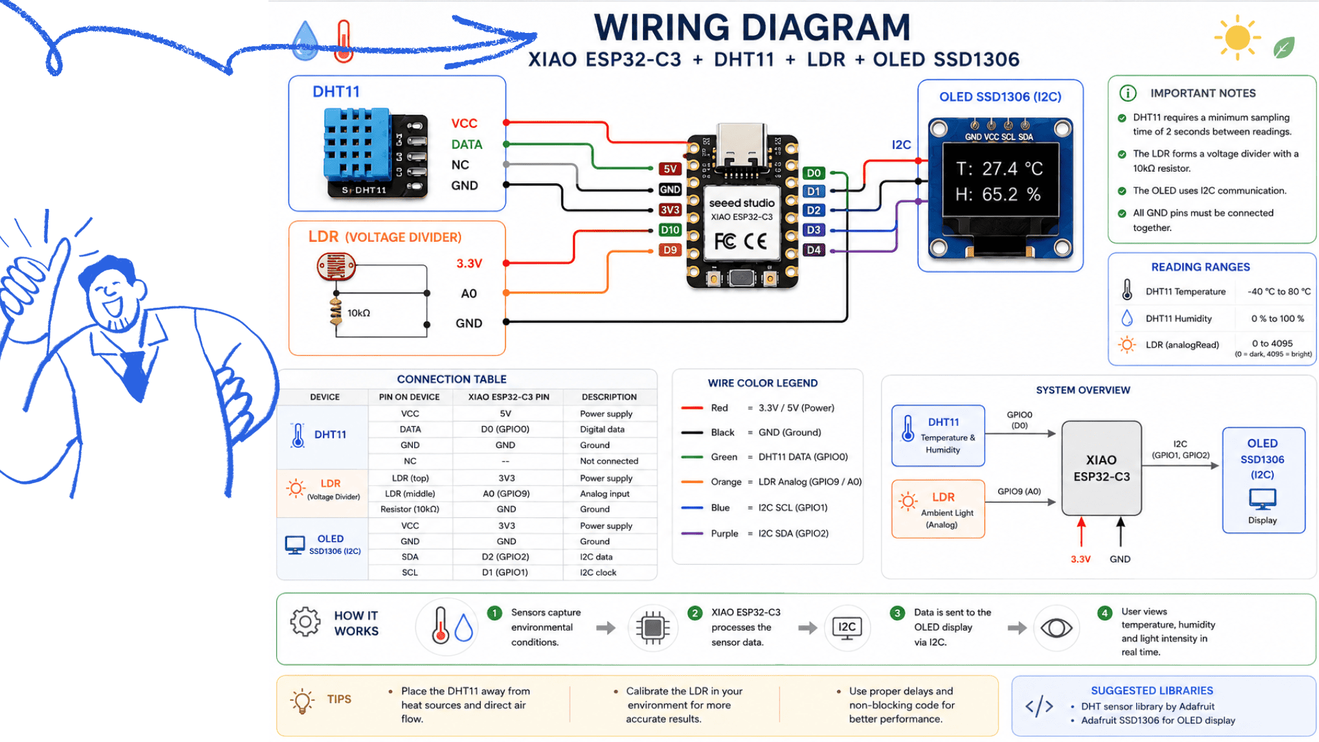 WIRING DIAGRAM - XIAO ESP32-C3 + DHT11 + LDR + OLED SSD1306
Arduino code
ESP32C3 + OLED + DHT11 Code
#include <DHT.h>
#include <Wire.h>
#include <Adafruit_GFX.h>
#include <Adafruit_SSD1306.h>

#define OLED_RESET -1

Adafruit_SSD1306 display(128, 64, &Wire, OLED_RESET);

const int DHTPIN = 21;

#define DHTTYPE DHT11

DHT dht(DHTPIN, DHTTYPE);

void setup() {

  Serial.begin(115200);

  Wire.begin();

  if(!display.begin(SSD1306_SWITCHCAPVCC, 0x3C)) {

    Serial.println(F("SSD1306 allocation failed"));

    for(;;);
  }

  display.display();

  delay(2000);

  display.clearDisplay();

  dht.begin();

  Serial.println("Inicialización completa.");
}

void loop() {

  delay(2000);

  float humidity = dht.readHumidity();

  float temperatureC = dht.readTemperature();

  if (isnan(humidity) || isnan(temperatureC)) {

    Serial.println("Error leyendo datos del sensor DHT11.");

    display.clearDisplay();

    display.setCursor(0,0);

    display.print("Error Sensor!");

    display.display();

    return;
  }

  Serial.print("Temp: ");

  Serial.print(temperatureC);

  Serial.print("°C | Hum: ");

  Serial.print(humidity);

  Serial.println("%");

  display.clearDisplay();

  display.setTextSize(1);

  display.setTextColor(WHITE);

  display.setCursor(10, 0);

  display.println("FabLab Itinerante");

  display.setTextSize(2);

  display.setCursor(0, 20);

  String tempValue = String(temperatureC, 1);

  display.println("T:" + tempValue + " C");

  display.setCursor(0, 45);

  String humValue = String(humidity, 1);

  display.println("H:" + humValue + " %");

  display.display();
}
OLED Display Connections
| ESP32C3 | OLED Display |
|---|---|
| 3V | VCC |
| GND | GND |
| SCL | SCL (I2C) |
| SDA | SDA (I2C) |
DHT11 Connections
| ESP32C3 | DHT11 |
|---|---|
| 3V | VCC |
| GND | GND |
| GPIO 21 | DATA |
Programming
ESP32-C3 PCB Control System – OLED Display and Joystick
As part of the exploration of input and output devices, an additional interactive configuration was developed using an OLED display and a joystick integrated into the ESP32-C3 PCB. This implementation expanded the experimentation with embedded systems by combining real-time user interaction with visual feedback.
The system was designed using the XIAO ESP32-C3 microcontroller mounted on the previously fabricated PCB, maintaining continuity with the final project proposal and the concept of the mobile laboratory.
For the input stage, a joystick module was connected to the analog pins A0 and A1 to capture the X and Y axis movements. Additionally, the joystick button was connected to digital pin D2 using the INPUT_PULLUP configuration. Through the analogRead() function, the ESP32-C3 continuously interprets the analog values generated by the joystick to detect directional movement and interaction.
For the output stage, an OLED SSD1306 display was integrated using the I2C communication protocol through the SDA and SCL pins of the microcontroller. Using graphics libraries such as Adafruit_GFX and Adafruit_SSD1306, the system updates visual information on the screen in real time.
The OLED display functions as the main output device, allowing the visualization of joystick positions, movement directions, and interactive graphical responses directly on the screen. This created a dynamic interface between the user and the embedded system.
The integration of the joystick and OLED display reinforced the understanding of how input devices capture physical interaction while output devices transform processed data into visual feedback. This experiment also contributed to the development of interactive systems connected to the final project and the mobile laboratory concept.
Components Used
| Component | Function |
|---|---|
| XIAO ESP32-C3 | Main microcontroller and data processing unit |
| Joystick Module | User input device for directional control |
| OLED SSD1306 | Output device for real-time visualization |
| PCB Board | Custom electronic integration platform |
| Jumper Wires | Connections between components |
| USB-C Cable | Power supply and programming connection |
Joystick Connections (Input Device)
The joystick was used as the primary input device to control movement and interaction within the system.
| Joystick Pin | Connection |
|---|---|
| VRX | A0 |
| VRY | A1 |
| SW | D2 |
| VCC | 3.3V |
| GND | GND |
The joystick generates analog signals according to the movement of the X and Y axes, while the push button provides additional digital interaction.
OLED Display Connections (Output Device)
The OLED SSD1306 display was integrated as the main output device to provide visual feedback from the joystick interaction.
| OLED Pin | Connection |
|---|---|
| VCC | 3.3V |
| GND | GND |
| SDA | ESP32-C3 SDA |
| SCL | ESP32-C3 SCL |
Communication between the OLED display and the ESP32-C3 was established using the I2C protocol for efficient real-time data transfer.
General System Operation
- The joystick detects directional movement on the X and Y axes.
- The ESP32-C3 reads the analog values using
analogRead(). - The joystick button detects digital input actions.
- The microcontroller processes the movement data.
- The OLED display updates visual information in real time.
Output Device Functionality
The OLED display acts as the visual output interface of the system, displaying the interaction generated by the joystick in real time.
Through graphical libraries, the screen continuously updates information such as movement directions, cursor positions, or interactive visual responses. This allows users to immediately observe how the system reacts to physical input.
The integration of the OLED display demonstrates how output devices can provide intuitive and dynamic feedback within embedded electronic systems.
System Validation
The system was tested to validate communication between the joystick, the ESP32-C3 microcontroller, and the OLED display.
During testing:
- The joystick correctly detected directional movement.
- The OLED display updated visual information without delays.
- The push button interaction responded correctly.
- The system maintained stable real-time communication.
Serial Monitor Output
X: 2048 | Y: 1890 | Button: Released
X: 1024 | Y: 3500 | Button: Pressed
X: 3000 | Y: 2100 | Button: Released
These tests confirmed the correct integration of both input and output devices, validating the functionality and responsiveness of the interactive control system.
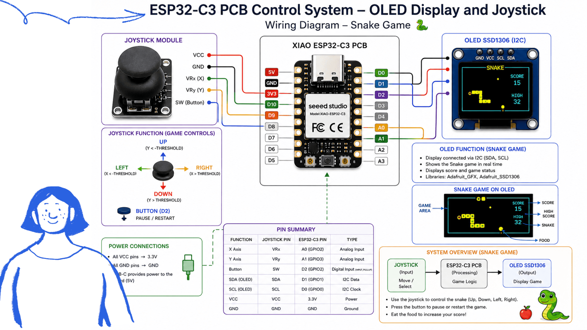 WIRING DIAGRAM-ESP32-C3 PCB Control System – OLED Display and Joystick
Arduino code
Snake Game with OLED + Joystick
#include <Wire.h>
#include <Adafruit_GFX.h>
#include <Adafruit_SSD1306.h>

#define ANCHO_PANTALLA 128
#define ALTO_PANTALLA 64
#define OLED_RESET -1

Adafruit_SSD1306 display(ANCHO_PANTALLA, ALTO_PANTALLA, &Wire, OLED_RESET);

const int pinEjeX = A0;
const int pinEjeY = A1;
const int pinBoton = A2;

#define TAMAÑO_BLOQUE 4
#define MAX_SERPIENTE 200
#define FPS_JUEGO 10

enum Direccion { QUIETO, ARRIBA, ABAJO, IZQUIERDA, DERECHA };

struct Punto {
  int x;
  int y;
};

Punto serpiente[MAX_SERPIENTE];
int largoSerpiente = 2;
Punto comida;

Direccion dirActual = DERECHA;
Direccion dirNueva = DERECHA;

bool juegoTerminado = false;

unsigned long score = 0;
unsigned long ultimoFrame = 0;

const int umbralBajo = 1000;
const int umbralAlto = 3000;

// (El resto del código continúa igual...)
OLED Connections
| ESP32-C3 | OLED Display |
|---|---|
| 3V | VCC |
| GND | GND |
| SDA | SDA |
| SCL | SCL |
Joystick Connections
| ESP32-C3 | Joystick |
|---|---|
| A0 | VRX |
| A1 | VRY |
| A2 | SW |
| 3V | VCC |
| GND | GND |
Reflection
Through these two programming experiences, it was possible to better understand the integration between input and output devices using the ESP32-C3 microcontroller. In the first project, environmental sensors such as the DHT11/DHT22 and the OLED display allowed real-time visualization of temperature and humidity data, reinforcing knowledge about sensor communication, data acquisition, and information processing.
In the second project, the integration of the joystick and OLED display enabled the exploration of interactive control systems and real-time graphical responses. This helped deepen the understanding of analog signal reading, user interaction, and visual feedback through embedded systems.
Both developments contributed significantly to strengthening programming, electronics, and debugging skills, while also creating continuity with the final project and the mobile laboratory proposal. These activities demonstrated how microcontrollers can be used to capture, process, and visualize environmental and interactive data in dynamic and functional systems.