Assignment Requirements
Group assignment
- Probe an input device(s)'s analog levels and digital signals (As a minimum, you should demonstrate the use of a multimeter and an oscilloscope..
- Document your work on the group work page and reflect on your individual page what you learned.
Individual assignment
- Design and document a parametric construction kit (consider kerf).Measure something: add a sensor to a microcontroller board that you have designed and read it.
Progress Status
This is for reporting progress (not for visitors to click).
Group page link + notes added.
Missing final photos and conclusions.
Upload .zip with source files.
Assignment Requirements
Learning outcomes
- Demonstrate workflows used in sensing something with input device(s) and MCU board
Have you answered these questions?
- Linked to the group assignment page.✅
- Documented what you learned from interfacing an input device(s) to your microcontroller and optionally, how the physical property relates to the measured results.✅.
- Documented your design and fabrication process or linked to the board you made in a previous assignment.✅.
- Explaind how your code works.✅.
- Explained any problems you encountered and how you fixed them.✅.
- Included original design files and source code.✅.
- Included a ‘hero shot’ of your board.✅.
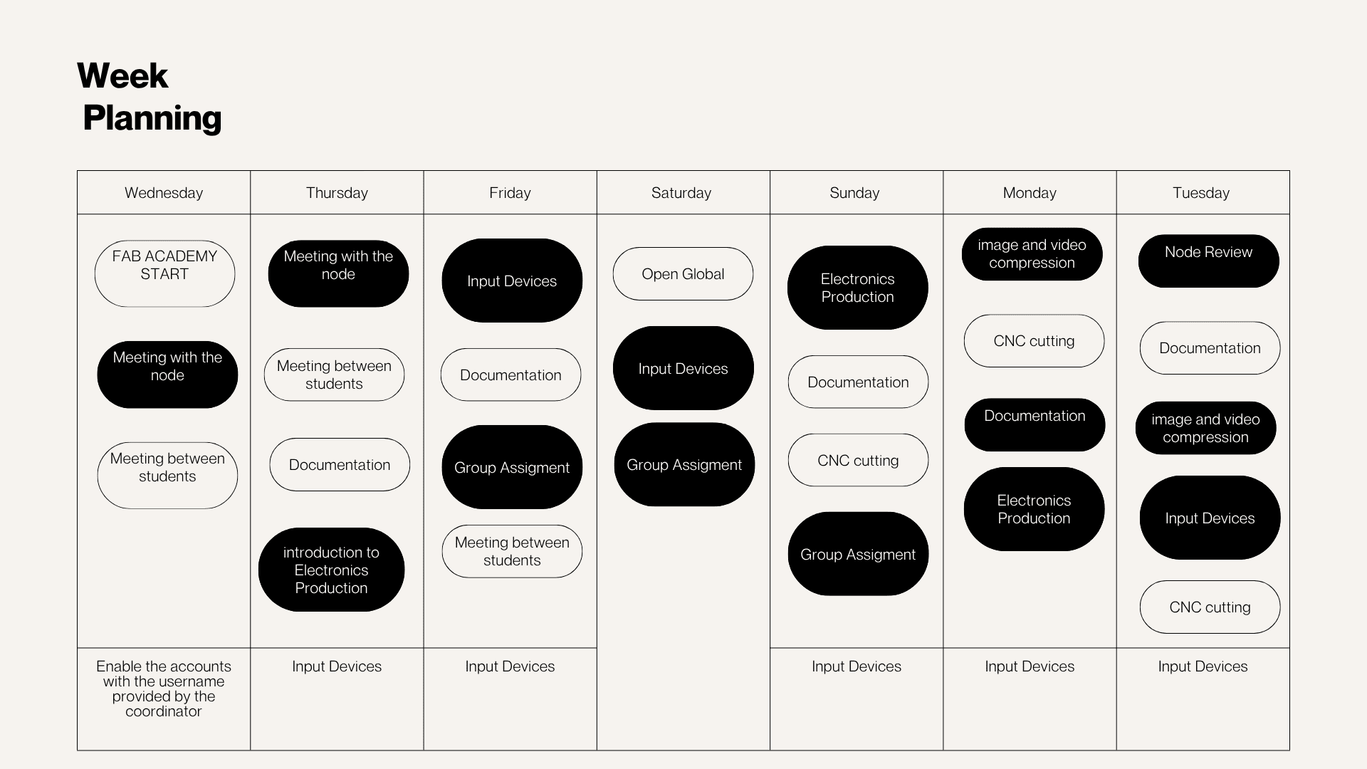
Weekly planning
During the week, we carried out various activities that presented significant challenges but were also very rewarding, especially due to the opportunity to share and learn as a team. We met virtually with our colleagues at the node and participated in lab meetings, which allowed us to organize ourselves and conduct open workshops in different spaces. In these sessions, we reviewed and worked with input devices, understanding their operation and their importance in capturing data from the environment for subsequent processing in electronic systems.
group work
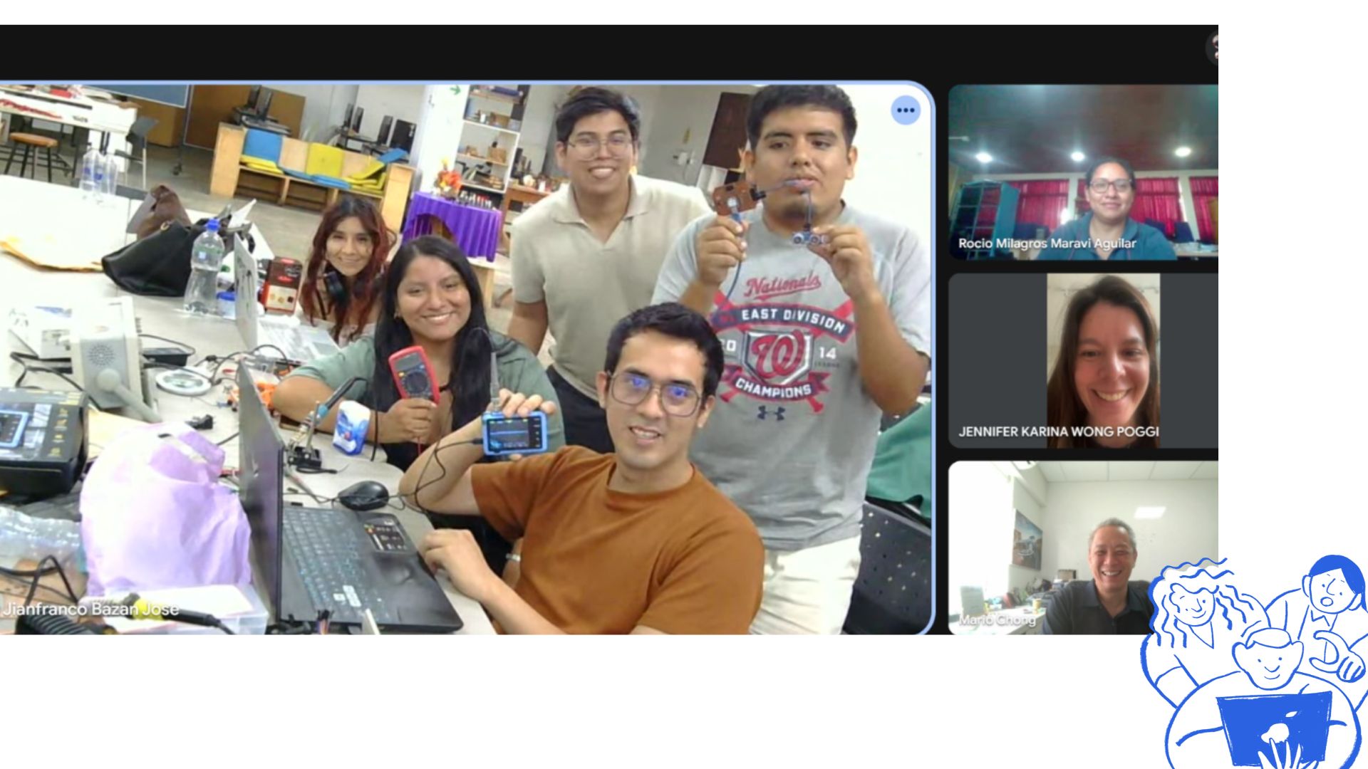
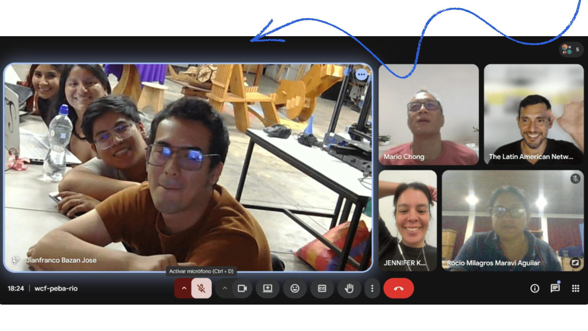
This week, focused on Input Devices, we held an in-person meeting at the Fab Lab UNI node. Colleagues in other cities also participated virtually, allowing the entire group to connect. In this stage, we worked with input devices, which capture information from the environment (such as light, temperature, or pressure) and transform it into signals that can be interpreted by electronic systems. We used various sensors and measuring tools for this purpose. During the practical sessions, we used equipment such as the oscilloscope and the multimeter, which helped us analyze electrical signals, verify voltages, and ensure the correct functioning of the circuits. These tools were essential for understanding how the sensors interact with the motherboard and how the data obtained is processed.
Group Project: Input Devices Analysis
In this group project, we used laboratory measurement tools to analyze input devices using a specially designed microcontroller board.
We tested a laboratory sensor and, using the microcontroller board, analyzed the signal with a multimeter and an oscilloscope.
Tools and Components Used
- Adrian Torres microcontroller board
- Seeed Studio XIAO RP2040
- HC-SR04 ultrasonic distance sensor
- LM393 photoresistor (LDR)
This experience allowed us to better understand how input devices capture and transmit data, as well as how signals can be measured and interpreted using laboratory equipment.
Procedures: Input Devices Analysis
You can view the complete group work here: View Group Project
Procedure 1: Digital Input (HC-SR04 Ultrasonic Sensor)
1. Description
The HC-SR04 ultrasonic module detects distance using Trigger and Echo pins. It sends a signal and measures the time it takes to bounce back.
- Range: 2 cm to 500 cm (15° angle)
- Accuracy: 0.3 cm increments
- Mounting: 4 holes on the board
- Formula: distance = (travel time / 2) × speed of sound
This step is important to ensure the board is safe and to avoid measuring a circuit with an accidental short.
2. Hardware and Software Setup
- 5V Supply
- Trigger (input)
- Echo (output)
- GND
Programmed using Arduino IDE with Xiao RP2040.
3. Signal Observation
After programming, we observed distance measurements, confirming:
- Correct operation of the HC-SR04 module
- Proper digital input signal behavior
Procedure 2: Analog Input (LM393 LDR Sensor)
1. Description
The LM393 photosensitive LDR sensor detects light intensity and provides both analog and digital outputs.
- Driving ability: 15mA with adjustable potentiometer
- Brightness: Adjustable sensitivity
- Detection: Light intensity
- Outputs: Analog and digital
This step is important to ensure the board is safe and to avoid measuring a circuit with an accidental short.
2. Hardware and Software Setup
- 5V Supply
- DO: Digital output
- A0: Analog output
- GND
Programmed using Arduino IDE with Xiao RP2040 and monitored through the Serial Monitor.
3. Signal Observation
After programming, we observed variations in light levels (low / no light), confirming:
- Correct operation of the LM393 LDR module
- Proper analog input signal behavior
Group Difficulties and Conclusions
Difficulties
- We were not familiar with the HC-SR04 and LM393 LDR modules, so we had to review their specifications.
- Incorrect connections caused the procedures to fail and took time to fix.
- Wrong pin selection (used D1 instead of D0), resulting in no data readings.
- After correcting connections and pins, we successfully measured distance and light intensity.
Conclusions
This group assignment helped us understand how to safely verify a board before measuring signals, correctly connect the oscilloscope, and interpret real digital signals in hardware. We also learned the importance of proper grounding, correct GPIO selection, and appropriate trigger and scale settings to obtain stable waveforms and validate the microcontroller’s operation.
group assignment
Individual Task
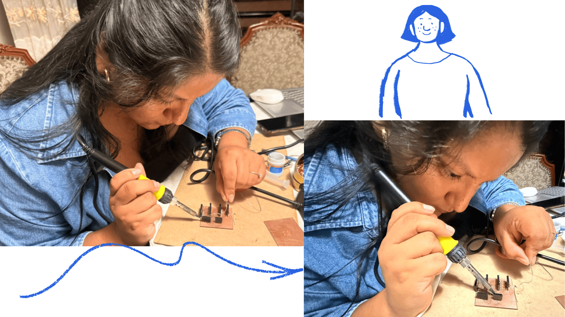
Individually, I conducted tests with sensors and simulations using a breadboard, the Wokwi platform, and a physical circuit board. This allowed me to validate the functionality of the components before their final implementation.
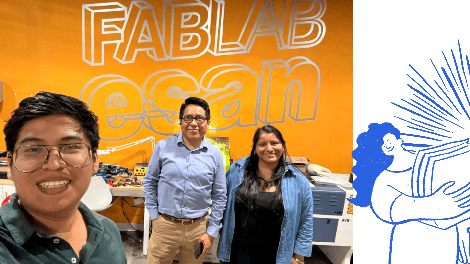
For the development of the circuit board, I attended the ESAN Fab Lab, where I was guided by Professor Jorge. This process presented a significant challenge, as we acquired knowledge about the operation of CNC machines from different perspectives each week.
On this occasion, we worked with the Carvera desktop CNC machine, which requires the use of additional software compared to other CNCs we had previously used. This necessitated a greater level of learning and adaptation.
We took as a reference the Silvana Espinoza board , since it contained components related to the final project I wanted to develop. In addition, Silvana guided us throughout the entire electronics development process, which helped me better understand the design and adaptation of the circuit. Based on this reference, I was able to customize the design according to my needs; however, achieving its correct adaptation and functionality also represented a challenge.
fairs for entrepreneurs and artisans.Fab Lab ESAN
test on a breadboard
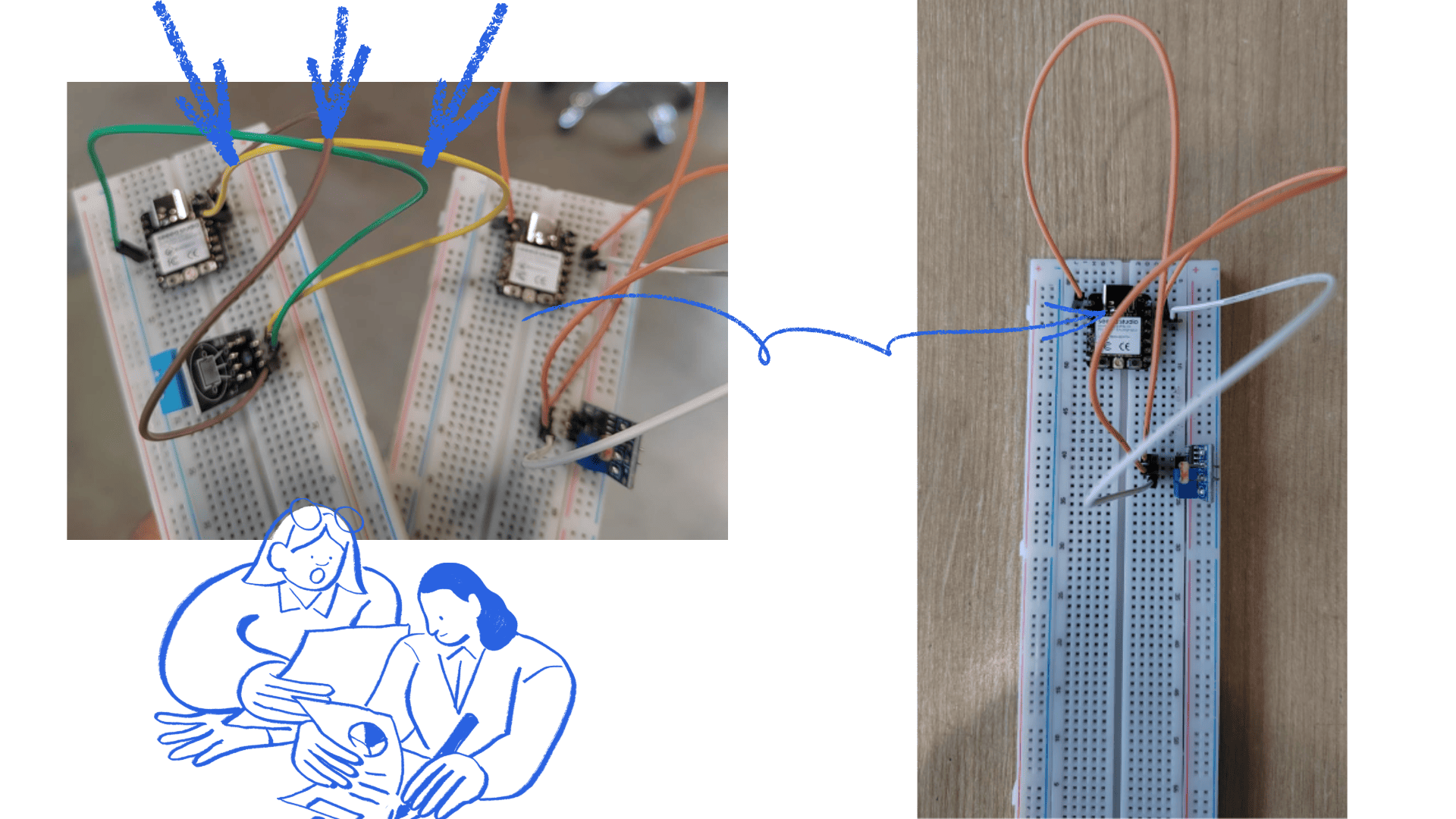
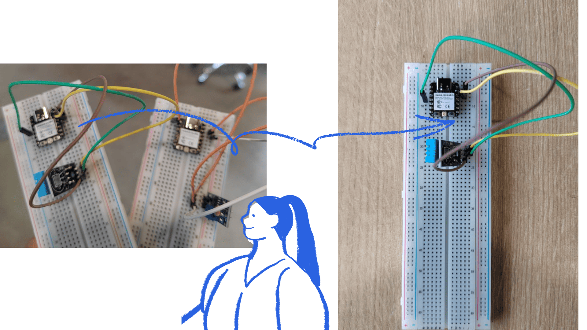
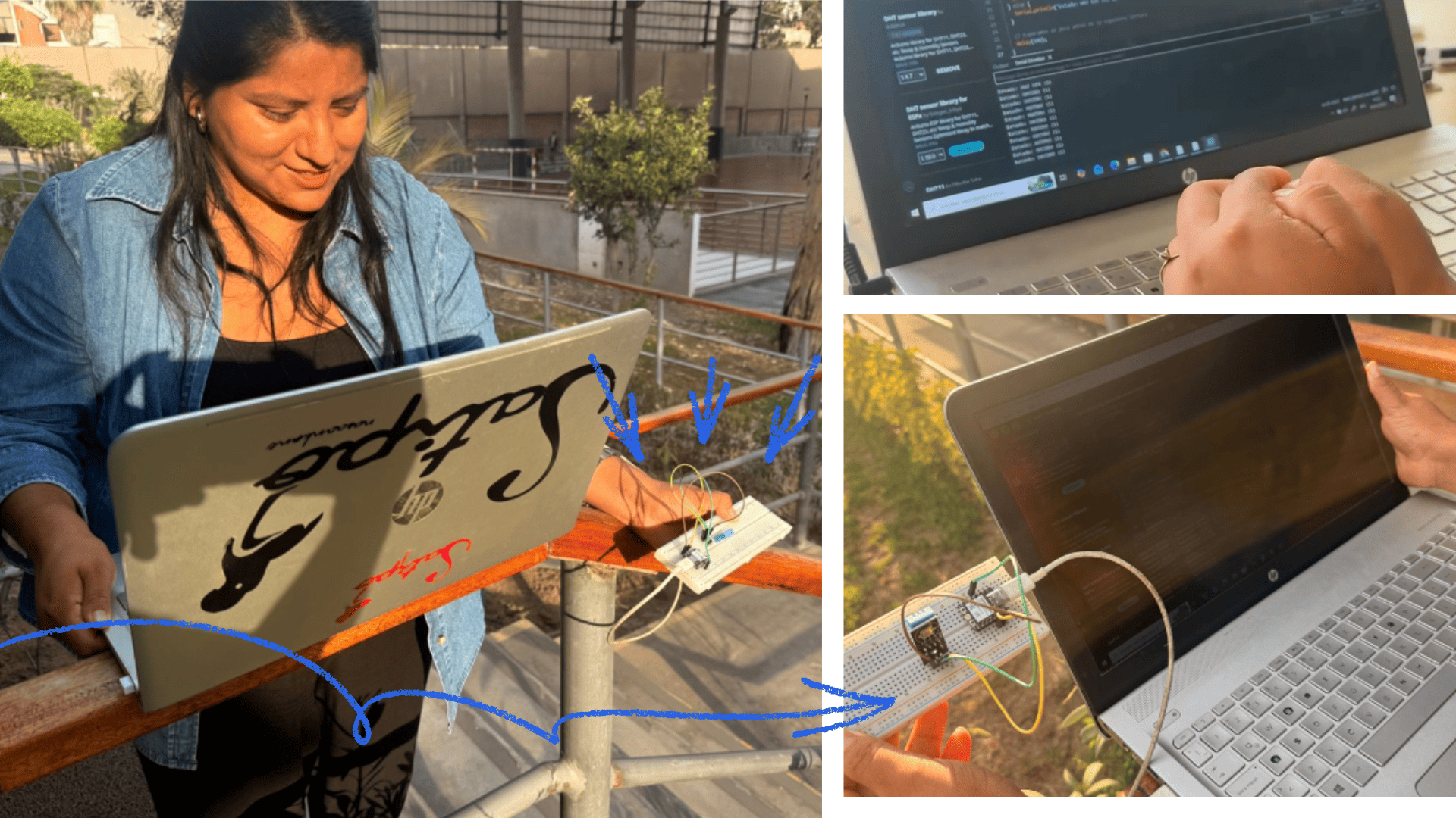
Before testing the sensors on the final PCB, a preliminary prototype was assembled on a breadboard as a practical testing stage. This allowed us to safely validate the circuit connections and verify the correct operation of each component before manufacturing the board.
A breadboard test was conducted to practice circuit assembly and, simultaneously, verify the correct operation of the sensors before their implementation on the final board.
For this test, the XIAO ESP32-C3 microcontroller was used along with various sensors, including a DHT11 for measuring temperature and humidity, and an LDR sensor for detecting light levels.
During the tests, the system's behavior was evaluated under different environmental conditions. Measurements were taken both indoors and outdoors, allowing for the observation of real-world variations in ambient temperature and humidity. Similarly, the LDR sensor responded correctly to changes in lighting, registering different values in the presence of bright light and in low-light conditions.
These breadboard tests were essential for validating the connections, verifying system stability, and detecting potential errors before board fabrication. Furthermore, they provided a better understanding of the sensors' behavior in real-world situations, facilitating the subsequent integration and optimization of the project.
Video (local)
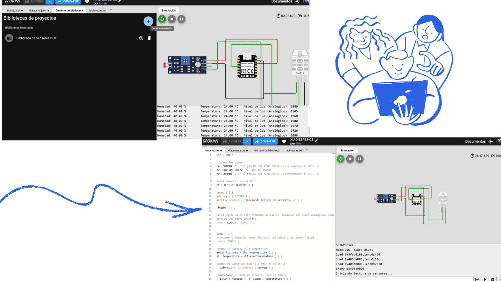
programming with wokwi
The programming was also done using the online platform Wokwi, which allows for the simulation of electronic circuits and the testing of code without the need for physical hardware. In this environment, the XIAO ESP32-C3 microcontroller was used, and various sensors were integrated to analyze its behavior in a virtual simulation.
Among the components used was the DHT11 sensor, responsible for measuring ambient temperature and humidity. Thanks to the simulation in Wokwi, it was possible to visualize the values generated by the sensor in real time, as well as verify the correct functioning of the code before implementing it on the physical board.
The use of Wokwi facilitated the detection of programming errors, allowing for quick adjustments to the code and optimization of the system logic. Furthermore, this tool offers advantages such as the simulation of multiple components, monitoring via the serial port, and the ability to work remotely, making it a very useful tool in the initial stages of electronic development.
Sensor Programming (DHT22 + LDR)
#include "DHT.h"

// Definimos los pines
#define DHTPIN 5
#define DHTTYPE DHT22
#define LDRPIN 2

// Inicializamos el sensor DHT
DHT dht(DHTPIN, DHTTYPE);

void setup() {
  Serial.begin(115200);
  Serial.println("Iniciando lectura de sensores...");

  dht.begin();

  pinMode(LDRPIN, INPUT);
}

void loop() {

  // Esperamos 2 segundos entre lecturas
  delay(2000);

  // Leemos humedad y temperatura
  float humedad = dht.readHumidity();
  float temperatura = dht.readTemperature();

  // Leemos el valor del LDR
  int valorLuz = analogRead(LDRPIN);

  // Verificamos errores de lectura
  if (isnan(humedad) || isnan(temperatura)) {
    Serial.println("¡Error al leer del sensor DHT!");
    return;
  }

  // Mostramos resultados
  Serial.print("Humedad: ");
  Serial.print(humedad);
  Serial.print(" %\t");

  Serial.print("Temperatura: ");
  Serial.print(temperatura);
  Serial.print(" °C\t");

  Serial.print("Nivel de luz: ");
  Serial.println(valorLuz);
}
Carvera Controller
First, open a web browser and go to the official Makera website. Then, locate the "Support" or "Downloads" section in the main menu. Within this section, search for the software called Carvera Controller.
Next, select the program version according to your computer's operating system (Windows or macOS) and click download. Once the file has downloaded, open the installer and follow the instructions to complete the installation.
Finally, run the Carvera Controller program to begin configuring and using your Carvera CNC machine.
Using the previously developed board in this assignment also allowed us to review several steps from the electronics production process, including board preparation, component integration, and system testing. This served as a solid foundation for the development and implementation of input devices, helping us better understand how sensors interact with the microcontroller and how data is processed within the system.
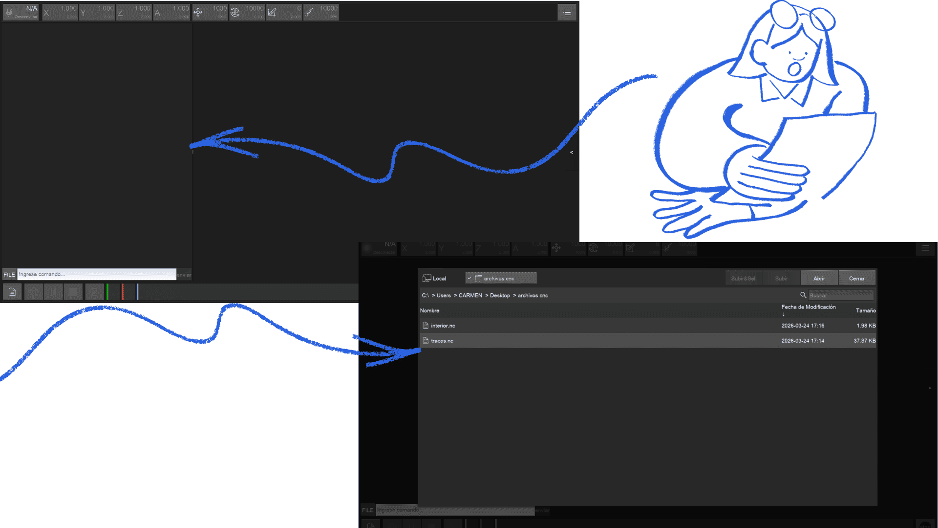
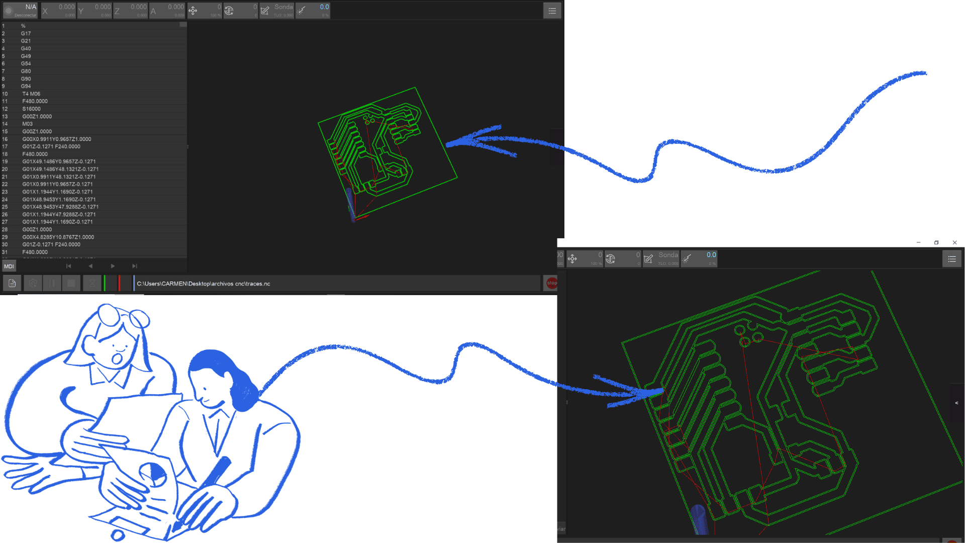
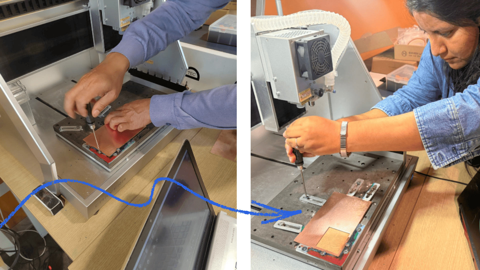
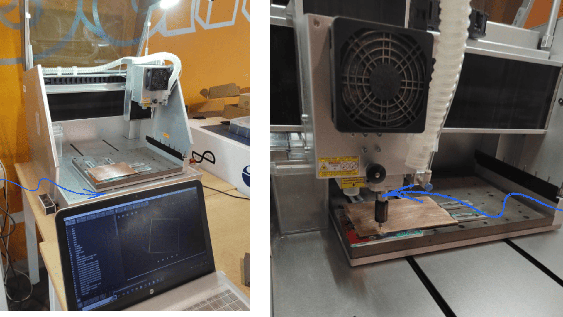
manufacturing of the plate on a Carvera CNC Machine
First, the board design is prepared in KiCad and the files are exported in Gerber format. These files are then converted to PNG or SVG using Gerber2PNG and processed in Mods to generate the machining toolpaths for both the internal traces and the external contour.
Next, the Carvera CNC machine is turned on and connected to the computer using the Carvera Controller software, ensuring it is properly calibrated.
The sacrificial bed is then positioned and checked, ensuring it is clean and level. The copper board (PCB) is placed on this surface and firmly secured with double-sided tape or clamps to prevent any movement during machining.
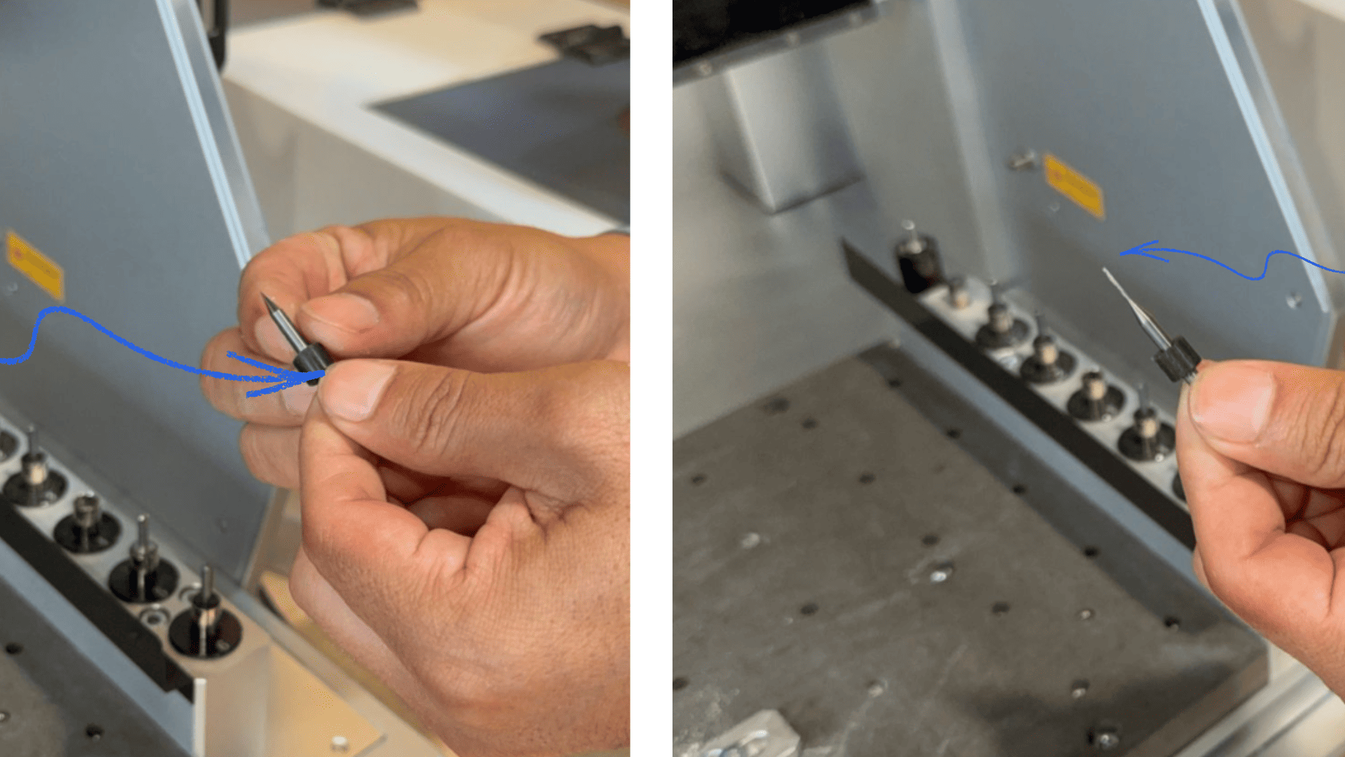
Then, the necessary milling tools are installed. The Carvera allows for automatic tool changes, so the tools are configured according to the type of work (internal traces and external cutting).
Next, the origin point is defined on the X, Y, and Z axes, either using the automatic probe or manually. This is essential to ensure the accuracy of the process.
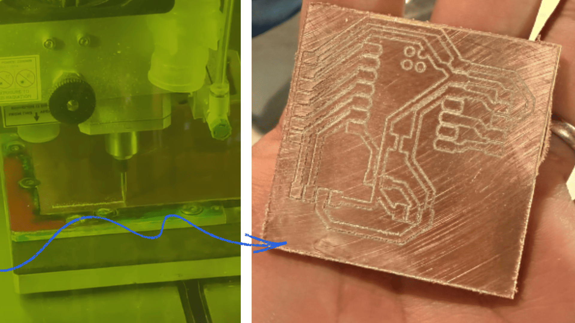
Once everything is configured, the toolpath files are loaded into the software, and machining begins. First, the internal tracks are milled, followed by the external cutting of the plate.
Finally, the plate is carefully removed, the surface is cleaned, and the connections and cuts are verified to ensure a high-quality final result.
Programming
For programming, the Arduino IDE development environment was opened. To ensure accurate readings from the DHT sensor, the corresponding library (DHT.h) was installed correctly.
First, the “Sketch” menu was accessed, then the “Include Library” option, and finally “Manage Libraries”. The term “DHT” was entered in the search box, which located the sensor library developed by Adafruit.
Once located, the “Install” option was selected, and the installation process was allowed to complete successfully. This step was essential to guarantee proper communication between the DHT sensor and the microcontroller.
This process is directly related to the use of input devices, since sensors such as the DHT22 and the LDR are capable of capturing environmental information, including temperature, humidity, and light intensity. These devices transform physical data from the environment into electrical signals that can be interpreted and processed by the microcontroller.
Likewise, this assignment helps generate continuity with the final project and the concept of the mobile laboratory, where these input devices will be used to collect real-time environmental information. The goal is to use this data to feed and visualize information on the web platform, creating an interactive system capable of monitoring environmental conditions through connected sensors.
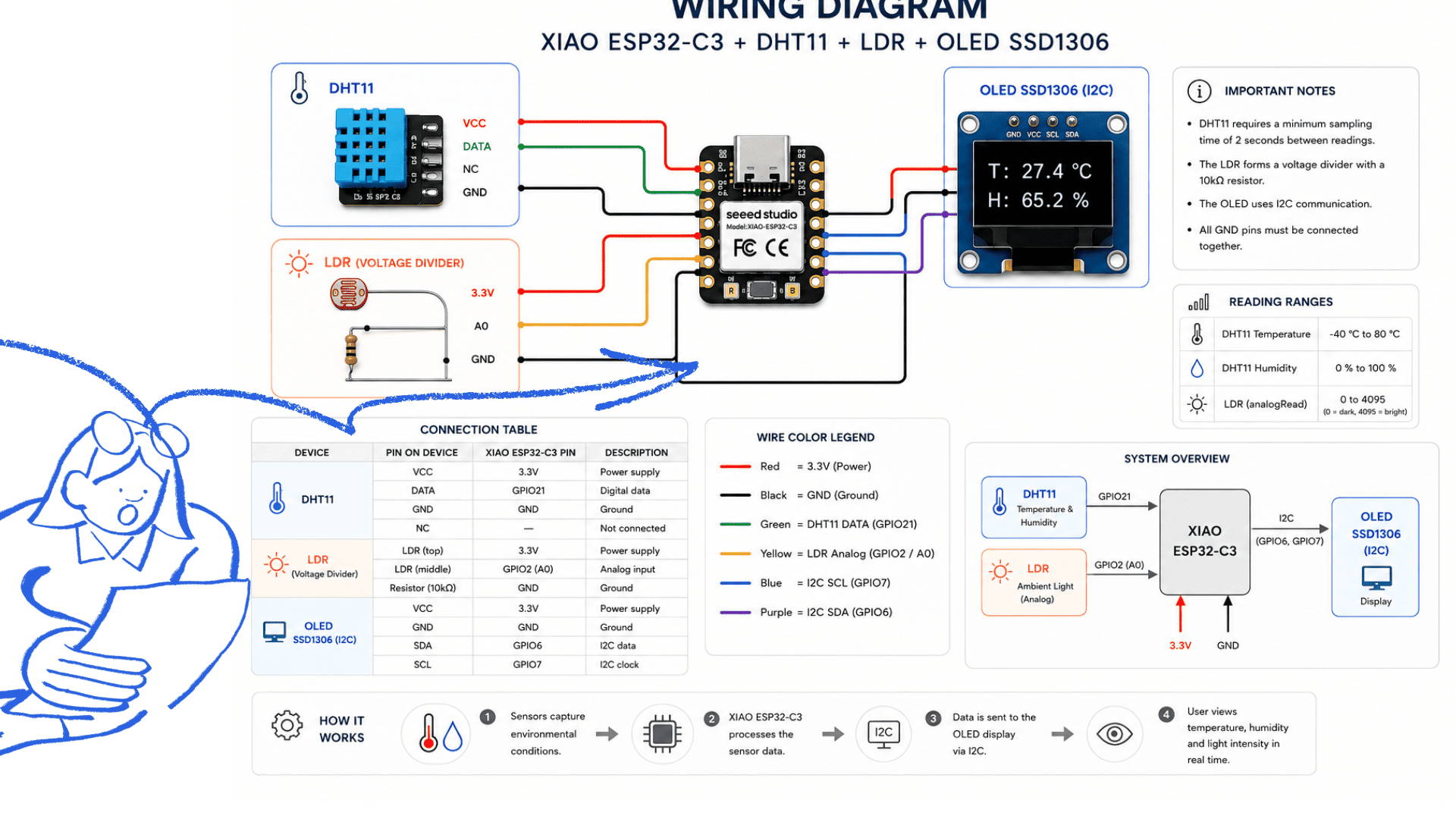
Components Used
| Component | Function |
|---|---|
| XIAO ESP32-C3 | Main microcontroller |
| DHT11 | Temperature and humidity sensor |
| LDR Sensor | Light intensity detection |
| OLED SSD1306 | Real-time data visualization |
| Resistors | Electrical stability |
| Jumper Wires | Connections between components |
| USB-C | Power supply and programming |
Component Connections
DHT11 Sensor
The DHT11 sensor was used to measure environmental temperature and humidity.
| DHT11 Pin | Connection |
|---|---|
| VCC | 3.3V |
| GND | GND |
| DATA | GPIO 21 |
The sensor sends digital data directly to the XIAO ESP32-C3 for processing.
LDR Sensor
The LDR sensor detects ambient light intensity using analog readings.
| LDR Pin | Connection |
|---|---|
| One side | 3.3V |
| Other side | ESP32-C3 Analog Pin |
| Resistor | GND |
The microcontroller uses analogRead() to interpret light intensity changes detected by the LDR.
OLED SSD1306 Display
The OLED display shows real-time sensor data.
| OLED Pin | Connection |
|---|---|
| VCC | 3.3V |
| GND | GND |
| SDA | ESP32-C3 SDA |
| SCL | ESP32-C3 SCL |
Communication is established using the I2C protocol.
General System Operation
- The DHT11 measures temperature and humidity.
- The LDR detects light intensity.
- The XIAO ESP32-C3 processes the sensor data.
- The information is displayed on the OLED screen.
- The serial monitor validates the readings in real time.
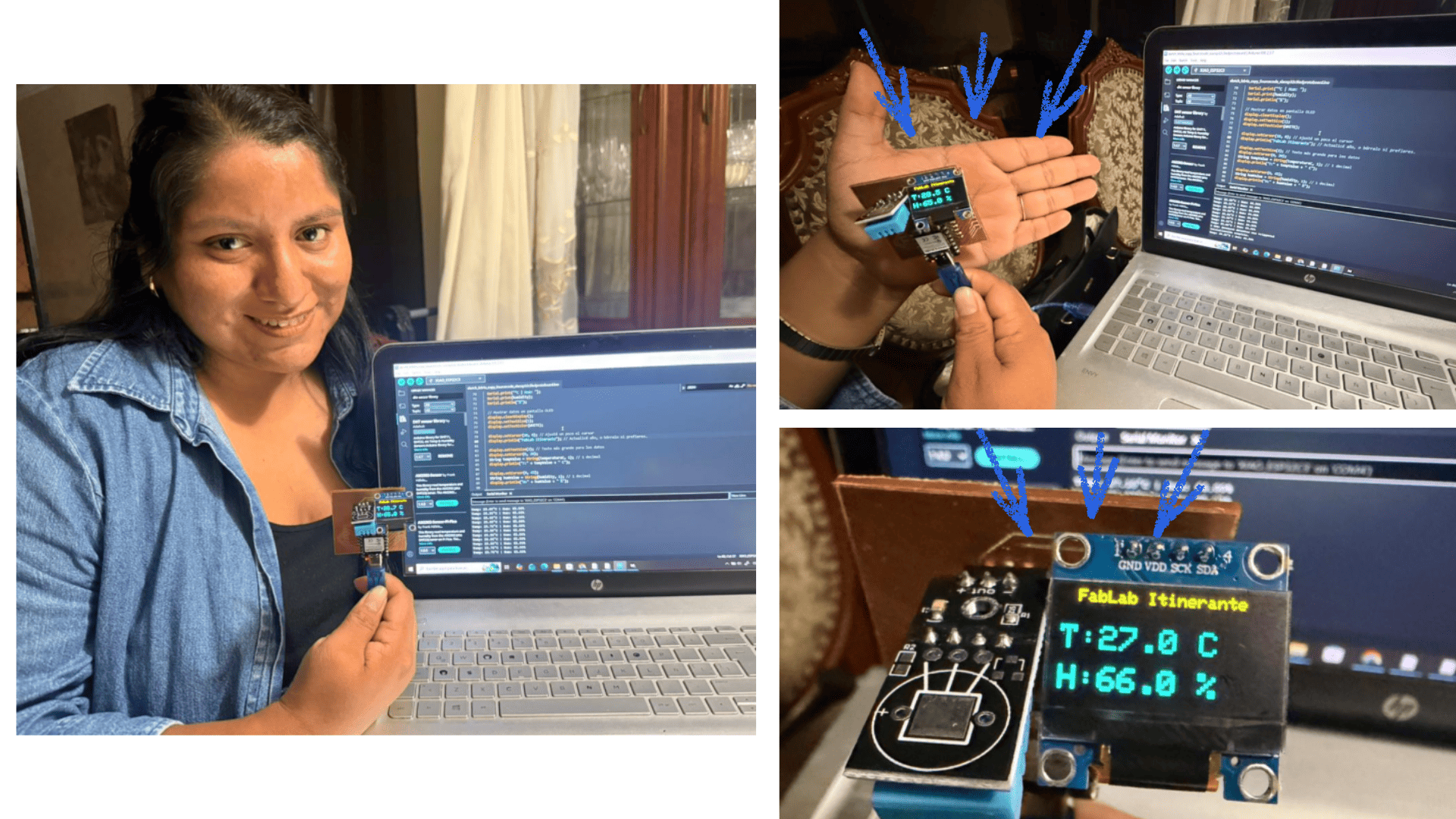
System Validation
The board was tested to validate communication between the XIAO ESP32-C3, DHT11 sensor, LDR sensor, and OLED display.
During testing:
- The serial monitor displayed stable readings.
- The OLED display correctly visualized the data.
- The system updated information every two seconds.
Serial Monitor Output
Initialization complete.
Temp: 27.4 C | Hum: 74.0%
Temp: 27.5 C | Hum: 73.0%
Temp: 27.6 C | Hum: 74.0%
These tests validated the correct operation of the system and the stability of the environmental readings.
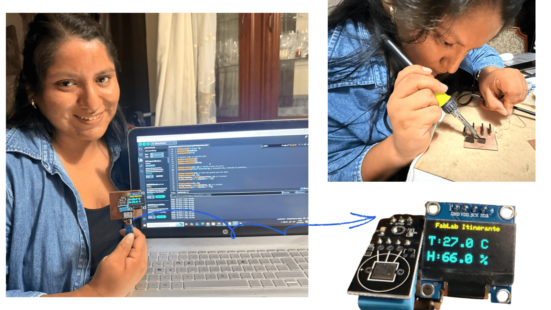
 ESP32C3 + OLED + DHT11 Programming
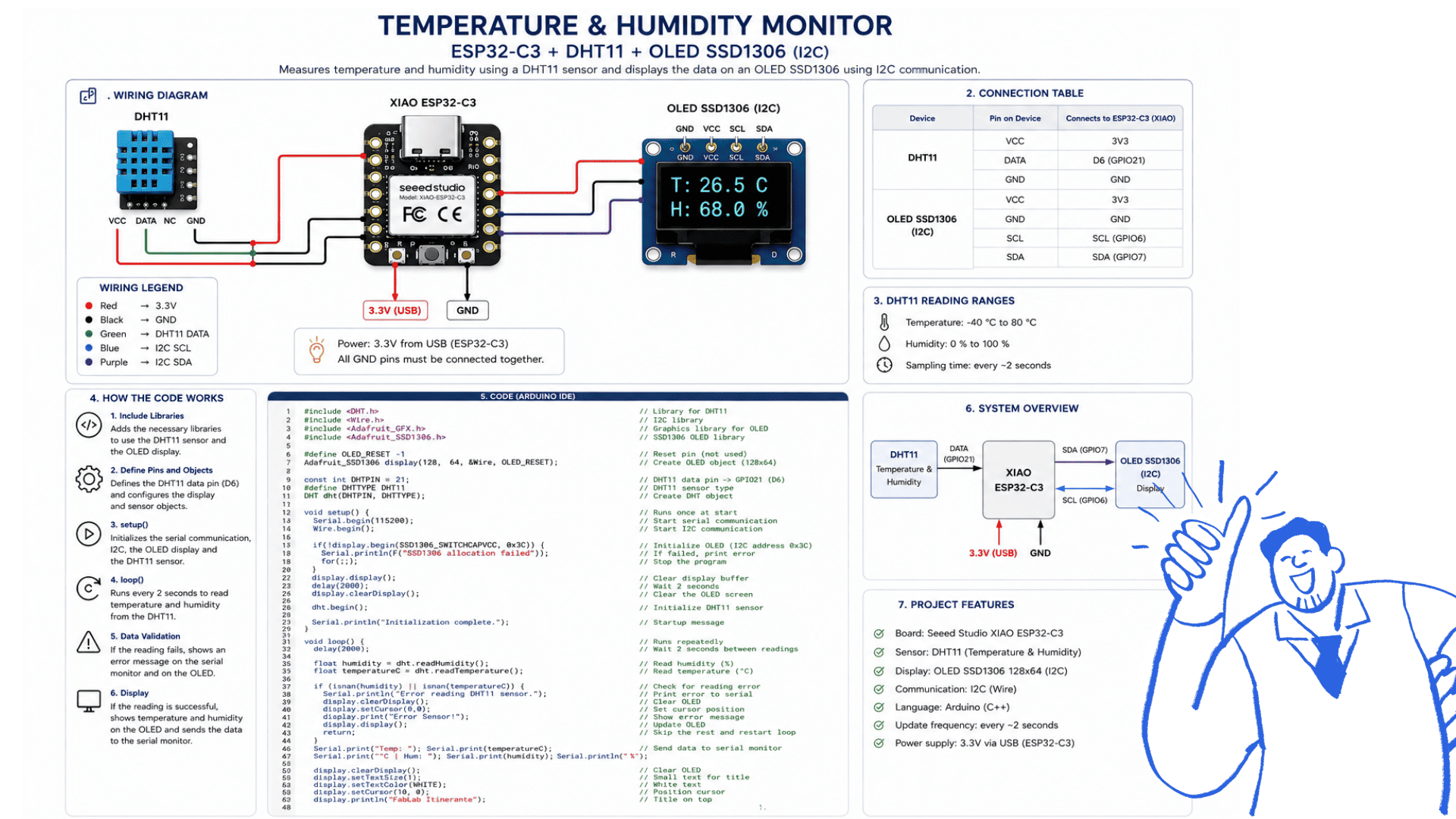 General System Operation
Arduino code
Code Explanation and Functionality
The code was developed in Arduino IDE to allow communication between the XIAO ESP32-C3, the DHT11 sensor, and the OLED SSD1306 display. The system successfully reads temperature and humidity data in real time and displays the information on both the Serial Monitor and the OLED screen.
First, the required libraries are included to control the sensor and the display:
#include <DHT.h>
#include <Wire.h>
#include <Adafruit_SSD1306.h>
The DHT11 sensor is connected to GPIO 21 and continuously sends environmental data to the ESP32-C3.
float humidity = dht.readHumidity();
float temperatureC = dht.readTemperature();
The instruction delay(2000) creates a two-second pause between readings.
This delay helps the DHT11 sensor provide stable and accurate data.
delay(2000);
The sensor values are processed and displayed on the Serial Monitor for validation:
Serial.print("Temp: ");
Serial.print(temperatureC);
Finally, the processed data is displayed on the OLED screen in real time:
display.println("T:" + tempValue + " C");
display.println("H:" + humValue + " %");
The code also includes error detection to identify invalid sensor readings and improve system reliability.
ESP32C3 + OLED + DHT11 Programming
/* ESP32C3             OLED DISPLAY
        3V   -------------  VCC
        GND -------------- GND
        SCL -------------- SCL
        SDA -------------- SDA

   ESP32C3              DHT11
        3V   ------------- 3V
        GND -------------- GND
        D6 --------------- DATA
*/

#include <DHT.h>
#include <Wire.h>
#include <Adafruit_GFX.h>
#include <Adafruit_SSD1306.h>

#define OLED_RESET -1
Adafruit_SSD1306 display(128, 64, &Wire, OLED_RESET);

const int DHTPIN = 21;

#define DHTTYPE DHT11

DHT dht(DHTPIN, DHTTYPE);

void setup() {

  Serial.begin(115200);
  Wire.begin();

  if(!display.begin(SSD1306_SWITCHCAPVCC, 0x3C)) {
    Serial.println(F("SSD1306 allocation failed"));
    for(;;);
  }

  display.display();
  delay(2000);

  display.clearDisplay();

  dht.begin();

  Serial.println("Inicialización completa.");
}

void loop() {

  delay(2000);

  float humidity = dht.readHumidity();
  float temperatureC = dht.readTemperature();

  if (isnan(humidity) || isnan(temperatureC)) {

    Serial.println("Error leyendo datos del sensor DHT11.");

    display.clearDisplay();
    display.setCursor(0,0);
    display.print("Error Sensor!");
    display.display();

    return;
  }

  Serial.print("Temp: ");
  Serial.print(temperatureC);
  Serial.print("°C | Hum: ");
  Serial.print(humidity);
  Serial.println("%");

  display.clearDisplay();
  display.setTextSize(1);
  display.setTextColor(WHITE);

  display.setCursor(10, 0);
  display.println("FabLab Itinerante");

  display.setTextSize(2);

  display.setCursor(0, 20);
  String tempValue = String(temperatureC, 1);
  display.println("T:" + tempValue + " C");

  display.setCursor(0, 45);
  String humValue = String(humidity, 1);
  display.println("H:" + humValue + " %");

  display.display();
}
OLED Display Connections
- VCC → 3V
- GND → GND
- SCL → SCL (I2C Bus)
- SDA → SDA (I2C Bus)
DHT11 Connections
- VCC → 3V
- GND → GND
- DATA → GPIO 21
Conclusions
During this assignment, it was possible to better understand how input devices work and how environmental data can be captured and processed using sensors and microcontrollers. The integration of the ESP32-C3, the OLED display, and the DHT11 sensor allowed the development of a functional system capable of monitoring temperature and humidity in real time.
Throughout the process, special attention had to be paid to software configuration, library installation, and component connectivity, since some errors required reinstalling and verifying the development environment. Despite these challenges, the system was successfully programmed and customized according to the project requirements.
- Connection configuration: The integration of the ESP32-C3, OLED display, and DHT11 sensor helped reinforce knowledge about electronic connections and communication protocols such as I2C.
- Library implementation: The use of libraries such as DHT.h and the OLED display libraries simplified sensor communication and graphical visualization of data.
- Relation to the final project: This assignment also contributes to the development of the mobile laboratory concept, where input devices will collect environmental information to later visualize and process the data through an interactive web platform.
Reflection
Developing the project using a breadboard, simulation in Wokwi, and the fabrication of the circuit board allowed for a comprehensive understanding of the electronic design process, from the initial idea to its physical implementation.
The use of the breadboard was fundamental for performing quick tests and validating connections in a real-world environment, allowing for the practical identification of errors before moving on to more advanced stages. It also allowed for the addition and testing of various sensors, which is directly related to my final project, facilitating experimentation with different configurations and components.
On the other hand, the simulation in Wokwi facilitated risk-free experimentation, helping to test the code, integrate components, and understand the system's behavior without the need for physical hardware. This allowed for multiple tests and adjustments to be performed quickly and efficiently.
Finally, the design and fabrication of the circuit board represented the most demanding stage, as it required greater precision, planning, and technical knowledge. This phase allowed for the consolidation of everything learned, integrating both electronic design and the manufacturing process.
Together, these tools and methodologies complement each other: simulation allows for anticipating errors, the breadboard validates functionality in practice, and the final board brings the project to life. This process not only strengthened technical skills but also problem-solving abilities and adaptability to difficulties, resulting in a functional and customized product aligned with the final project objectives.