Assignment Requirements
Group assignment
- Use the test equipment in your lab to observe the operation of a microcontroller circuit board (as a minimum, you should demonstrate the use of a logic analyzer).
- Document your work on the group work page and reflect what you learned on your individual page.
Individual assignment
- Use an EDA tool to design a development board that uses parts from the inventory to interact and communicate with an embedded microcontroller
Progress Status
This is for reporting progress (not for visitors to click).
Group page link + notes added.
Missing final photos and conclusions.
Upload .zip with source files.
Assignment Requirements
Learning outcomes
- Select and use software for circuit board design
- Demonstrate workflows used in circuit board design.
Have you answered these questions?
- Linked to the group assignment page✅
- Documented what you have learned in electronics design✅.
- Checked your board can be fabricated.✅.
- Explained problems and how you fixed them.✅.
- Included original design files (Eagle, KiCad, etc.).✅.
- Included your hero shots.✅.
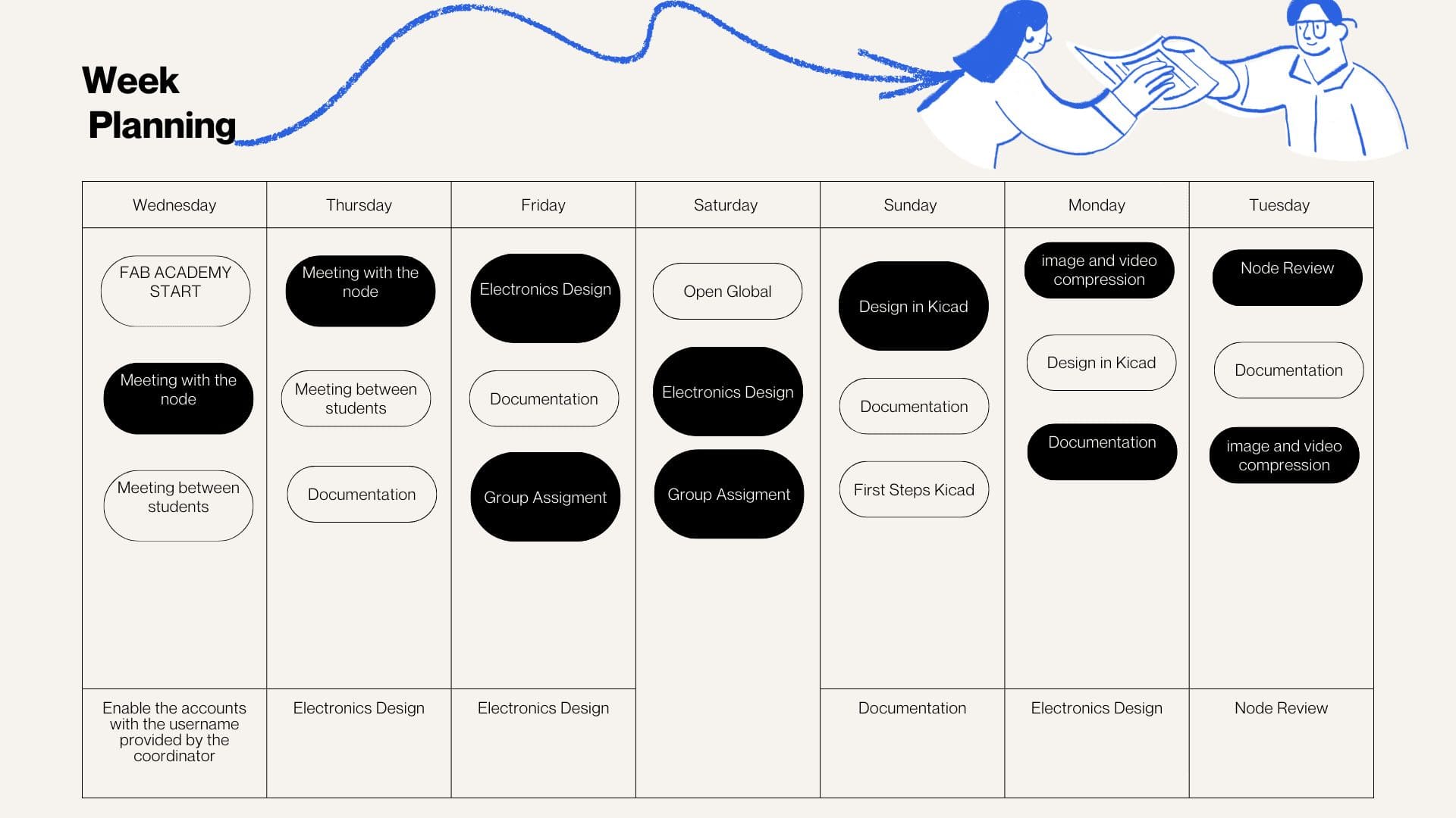
Weekly planning
During the week, we carried out various activities that presented significant challenges but were also very rewarding, especially due to the opportunity to share and learn together. We met virtually with our colleagues in the node and also participated in Open Lab meetings with Iquitos, Satipo, and Lima, which allowed us to organize and conduct open workshops in the different labs. In these sessions, we were able to review the software necessary for the work, as well as the machines, materials, and instruments required for each activity. This experience strengthened coordination between nodes and allowed us to better understand the importance of planning and managing resources effectively in digital fabrication processes.
Introduction to Electronics Design
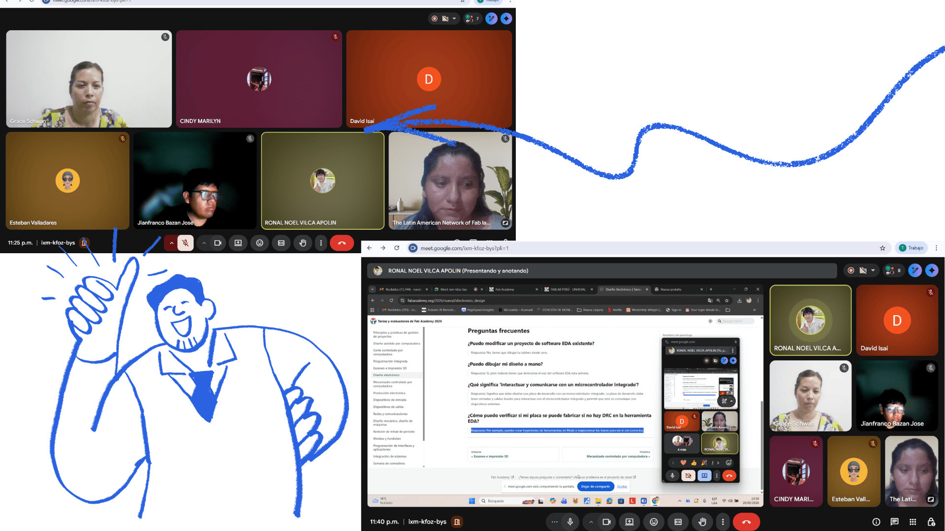
The topic of Electronics Design was completely new to me and the other members of my group. Thanks to Ronald's support, we were able to better understand the initial concepts. He provided us with a clear introduction, a practical example, and support in using the program, which facilitated our learning and allowed us to move forward with greater confidence this week.
group work
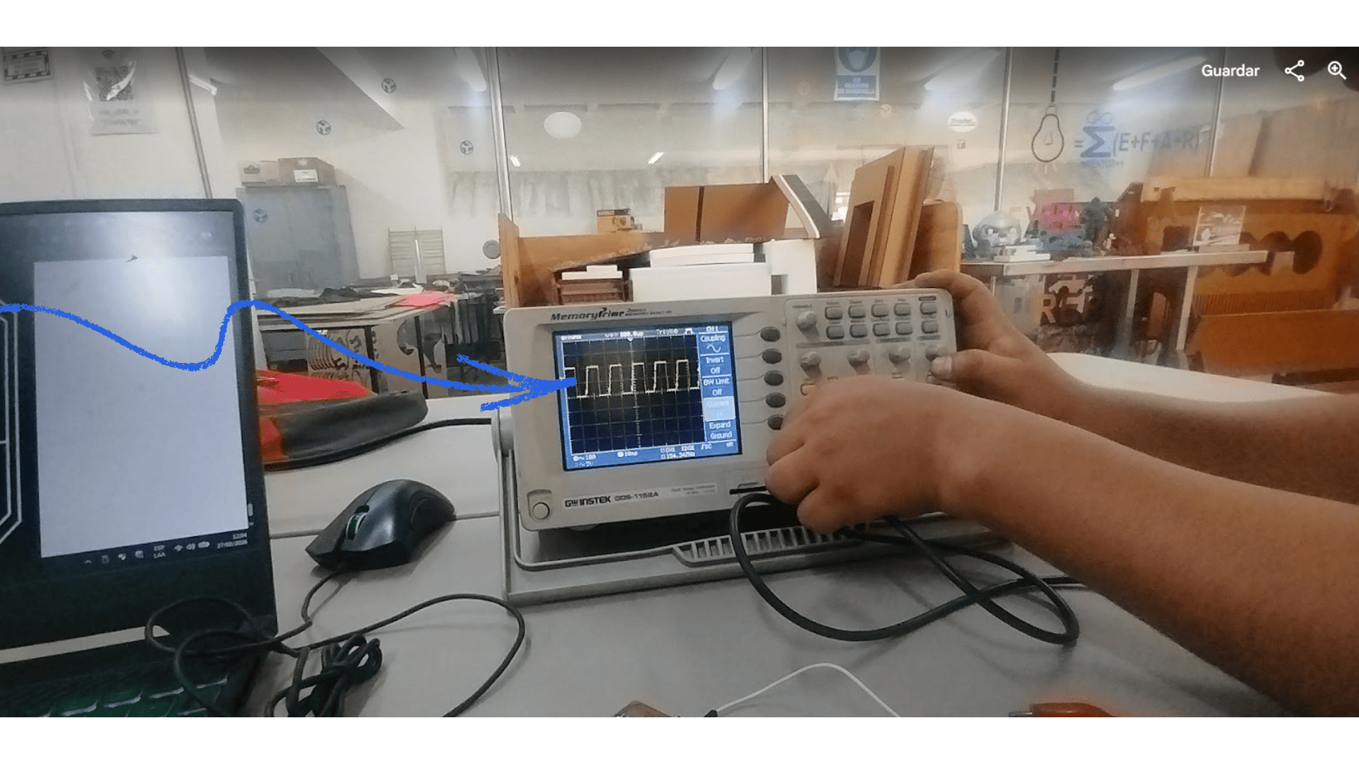
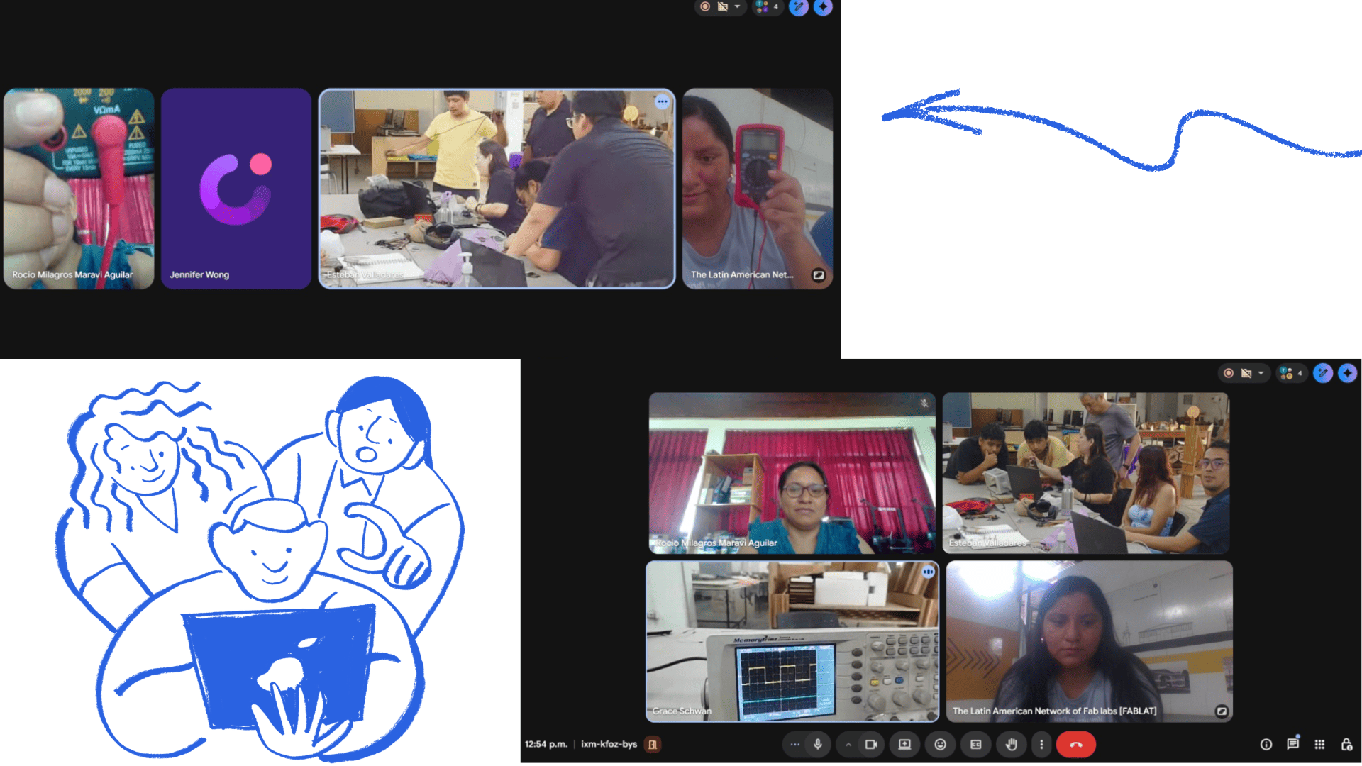
The objective of this group task was to observe and analyze the electrical behavior of a microcontroller board using laboratory measurement tools. We focused on verifying the stability of the power supply and confirming that the board can generate a reliable digital signal. For more detailed information, please visit the group page: View Group Work.
Personal Reflection
Using both the multimeter and the oscilloscope helped me better understand how electronic signals behave in real time. At first, I found it challenging to correctly configure the oscilloscope and obtain a stable waveform, but by following a step-by-step approach—starting with verifying power using the multimeter and then adjusting the oscilloscope settings—I was able to clearly visualize the signal. This experience showed me the importance of proper measurement techniques and careful setup. I also realized that small mistakes, such as incorrect grounding or probe configuration, can significantly affect the results. Overall, working with these tools improved my confidence in diagnosing circuits and reinforced the value of systematic troubleshooting in electronics.
Individual Assignment
Circuit Board Design in KiCad
Project: XIAO ESP32-C3 + Humidity/Temperature Sensor + LED Display
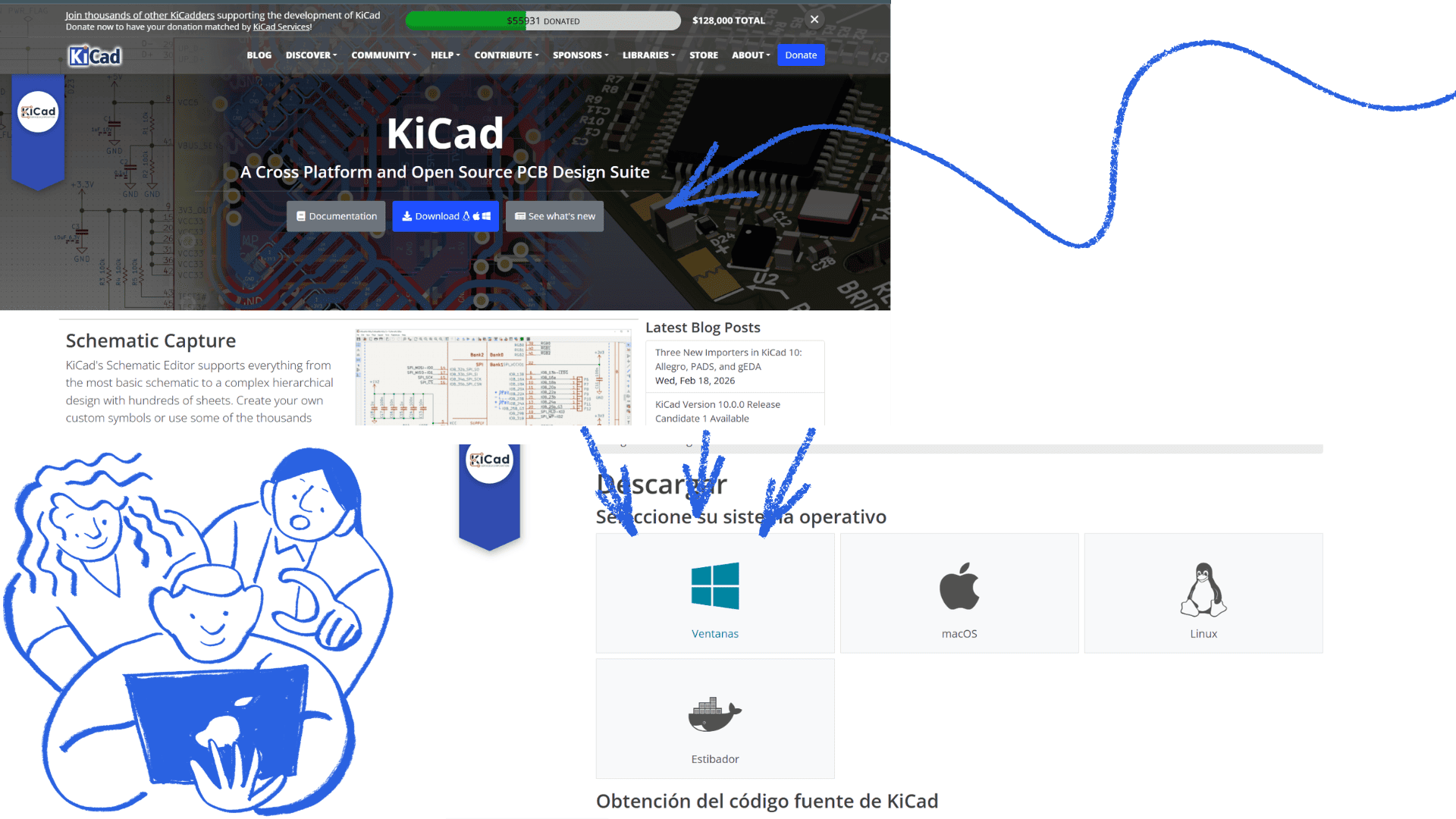
1. Download and Install KiCad
Go to the official KiCad website (https://www.kicad.org).
Click on Download and select the version compatible with your operating system (Windows, macOS, or Linux).
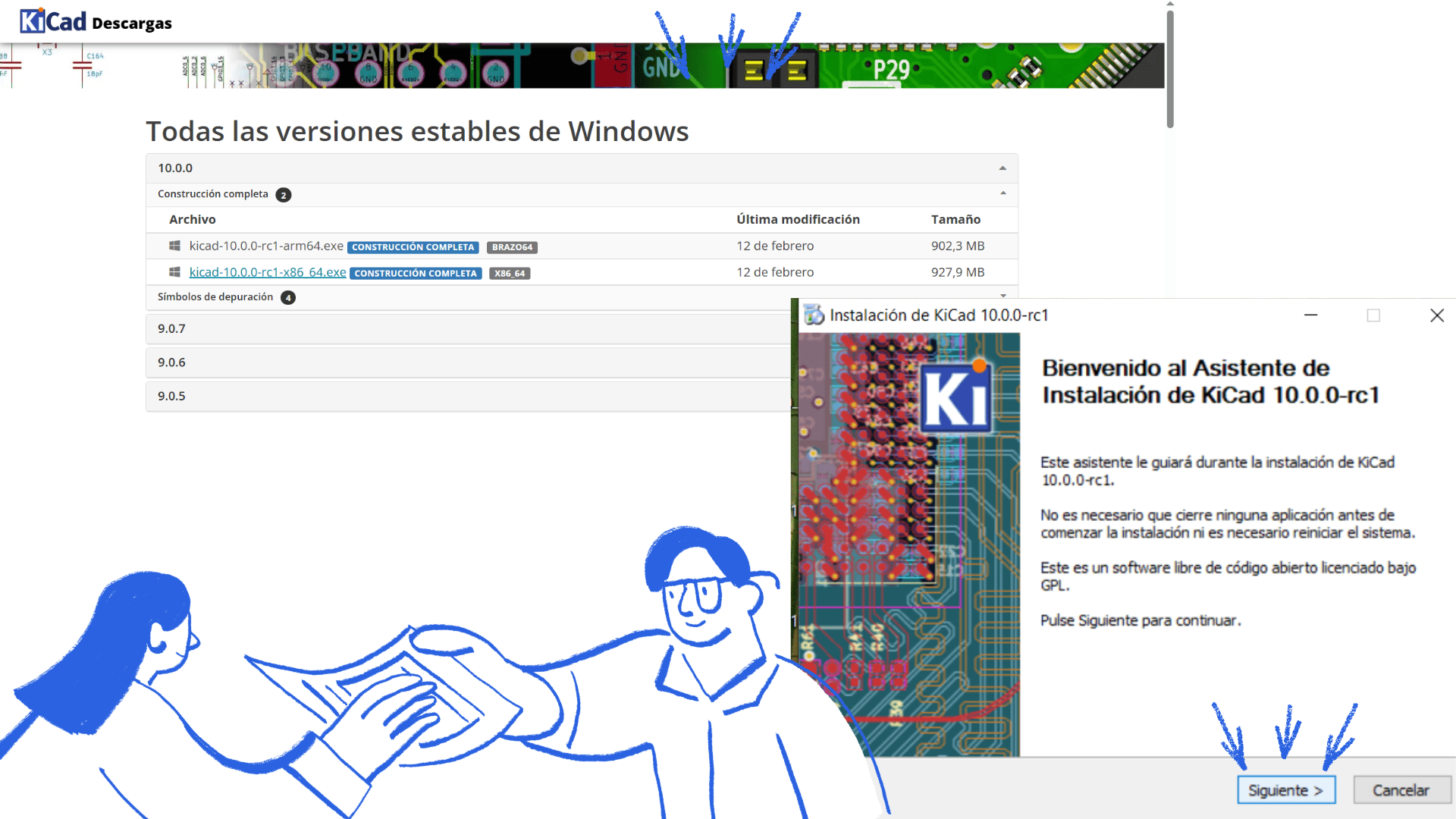
Download the installer and run the installation file.
Follow the installation steps using the default configuration options.
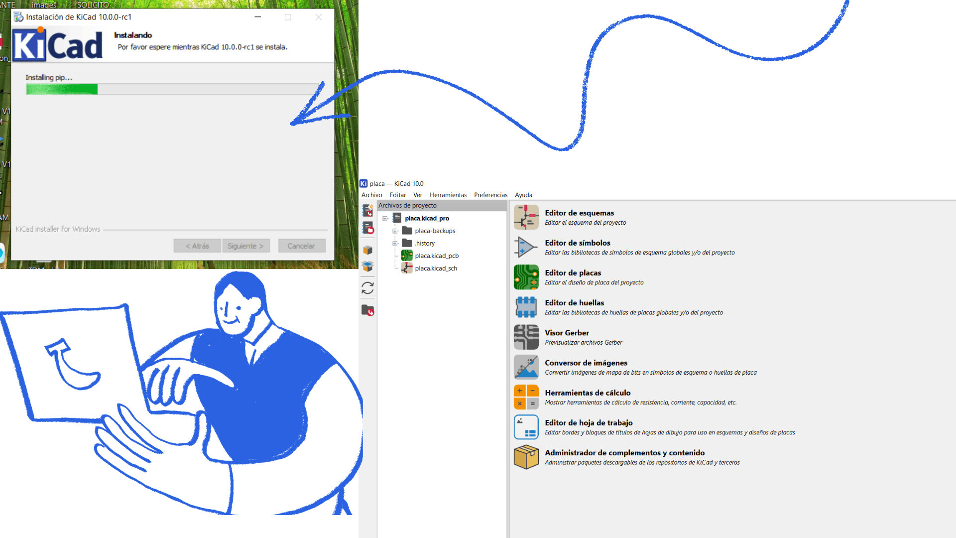
Make sure to install the standard symbol and footprint libraries.
Once installed, open KiCad and verify that the main tools are available: Schematic Editor, PCB Editor, Symbol Editor, and Footprint Editor.
2. Create a New Project and Work Sheet
Open KiCad.
Click on File → New Project.
Name the project: XIAO_ESP32C3_Sensor_Display.
Select an organized folder where the project files will be saved.
Click Save.
KiCad will automatically create the project files and generate a schematic file (.kicad_sch) and a PCB file (.kicad_pcb).
Open the Schematic Editor to access the work sheet.
This sheet is where you will design and connect all electronic components.
KiCad installation
KiCad installation
KiCad installation
KiCad
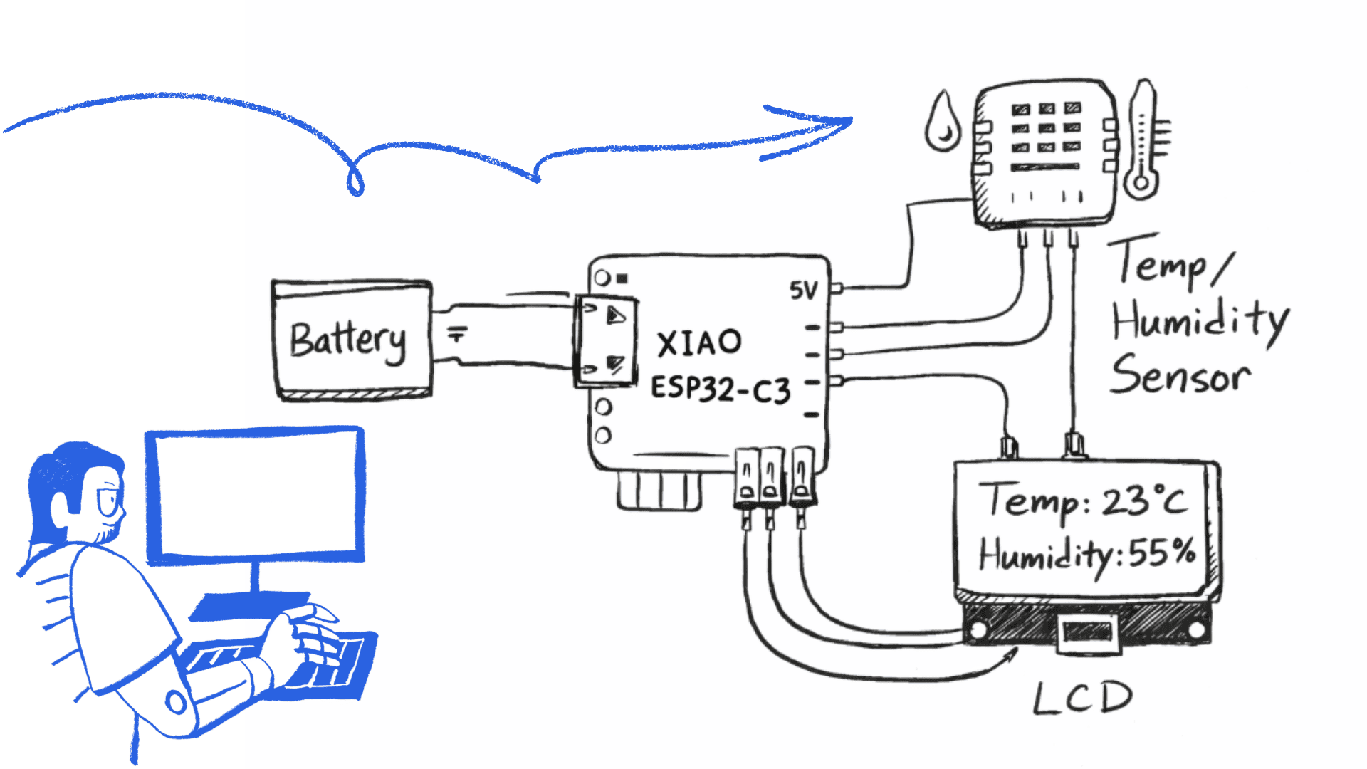
Electronics Design – Hand Sketch (Initial Plan)
Project: Environmental Monitoring System for a Mobile Laboratory
This electronic design is part of the mobile laboratory project and aims to develop a portable environmental monitoring system based on a XIAO ESP32-C3 microcontroller. This system will measure key variables such as temperature and humidity in each community visited, in order to gather relevant information for biomaterials research and development.
The device will consist of:
- A XIAO ESP32-C3 microcontroller as the main controller.
- A temperature and humidity sensor (e.g., DHT22 or BME280).
- An LED or OLED display to visualize the data in real time.
- A rechargeable battery for ease of use in the field.
General Operation
The sensor will capture environmental data (temperature and humidity) from the surroundings. This data will be processed by the XIAO ESP32-C3, which will display the information on the screen and allow the data to be stored or transmitted for digital recording.
Main Purpose of the System
- Obtain specific environmental information for each community visited.
- Analyze how climatic conditions influence the production of biomaterials.
- Customize biomaterial recipes according to local conditions (humidity and temperature).
- Provide real-world data to our biomaterials website, strengthening the project's technical and scientific information base.
This initial design (hand sketch) represents the conceptual stage of the project, where the system's general architecture is defined before moving on to the schematic design in software (KiCad) and the subsequent fabrication of the electronic board.
The mobile laboratory will benefit from this system by having measurable and verifiable data, allowing for process adaptation, improved results, and the generation of contextualized knowledge for each region.
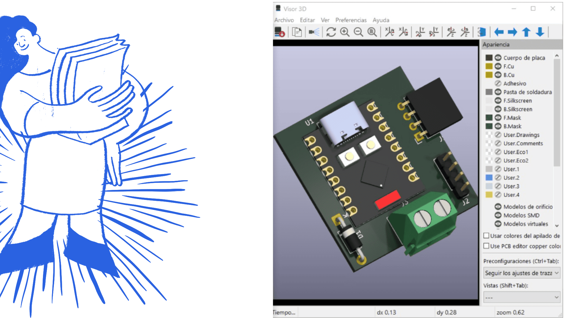
Circuit Board Design in KiCad
Project: XIAO ESP32-C3 + Humidity/Temperature Sensor + LED Display
1. Open the Project and Create the Schematic Sheet
Open KiCad and load your existing project (XIAO_ESP32C3_Sensor_Display).
Click on Schematic Editor to open the schematic work sheet.
This sheet is where you will design the electronic circuit and define all connections.
2. Add the Main Components to the Schematic
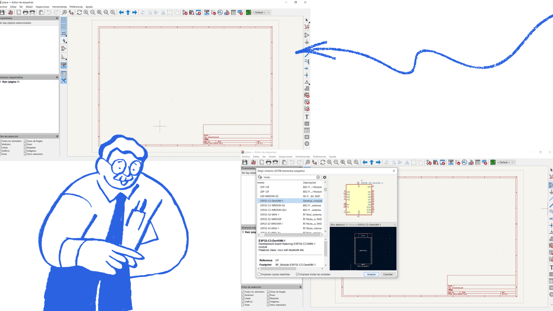
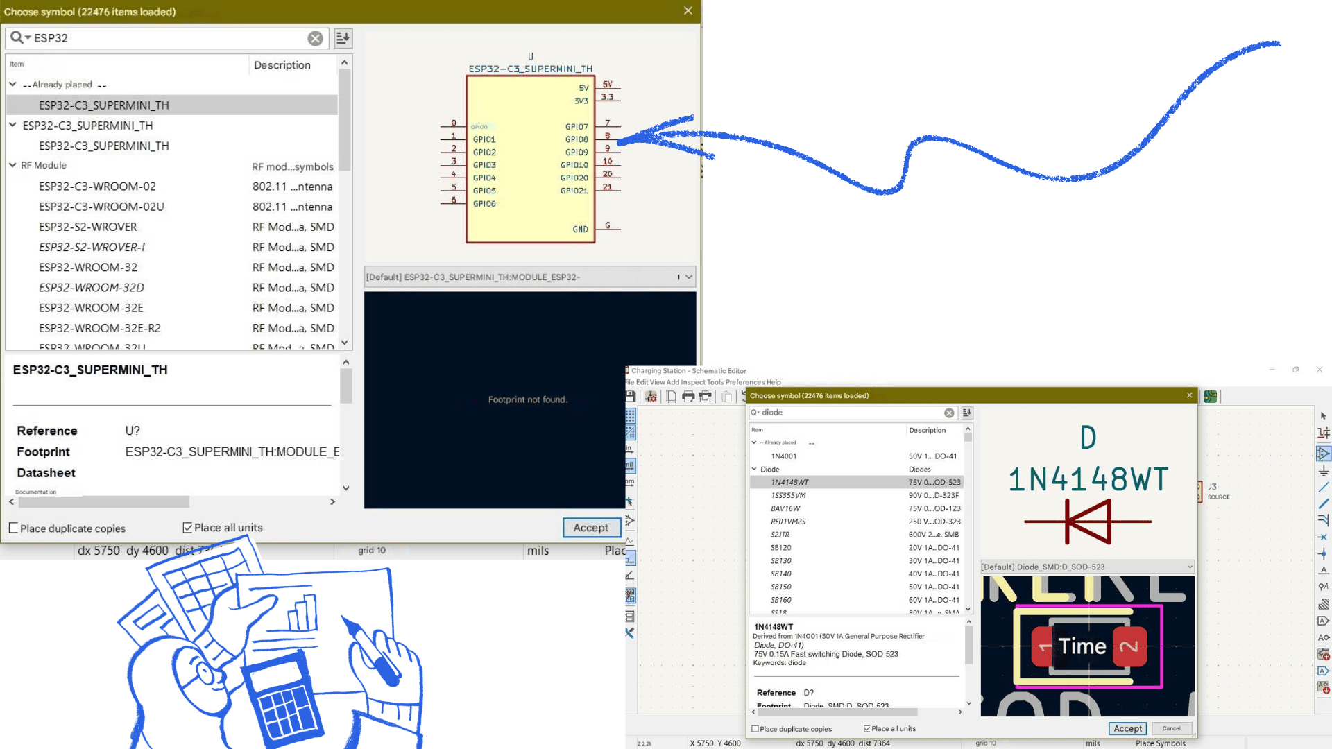
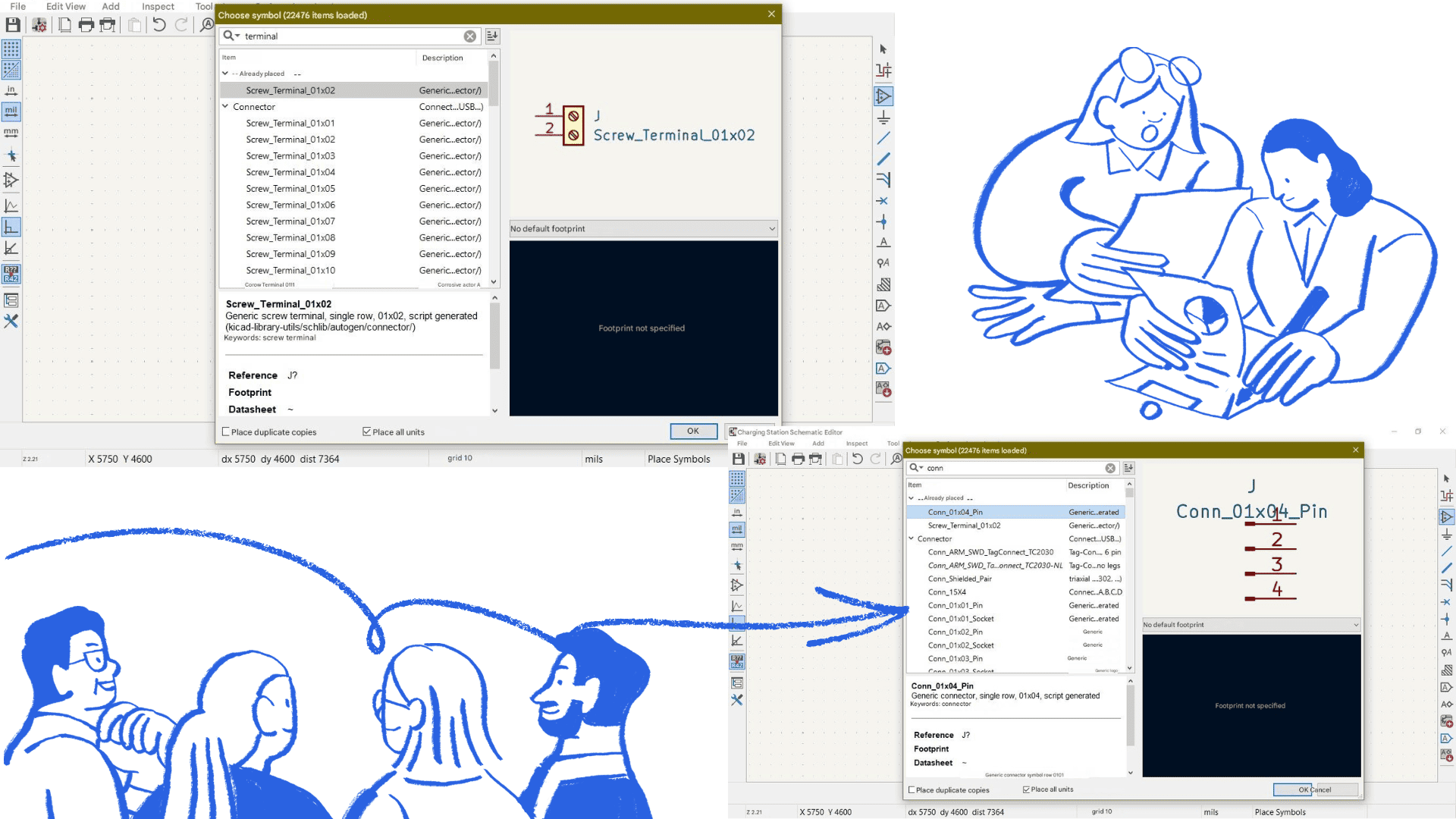
Click on Add Symbol and place the following components:
- XIAO ESP32-C3 (or a generic ESP32-C3 module if the exact symbol is not available).
- Temperature and humidity sensor (DHT22 or BME280).
- OLED Display (I2C) or LED display module.
- Resistors (10kΩ pull-up if using DHT22).
- 0.1µF decoupling capacitors between 3.3V and GND.
- Power symbols (3.3V and GND).
3. Design the Power Connections
Connect the 3.3V pin of the XIAO ESP32-C3 to:
- Sensor VCC
- Display VCC
Connect all GND pins together to create a common ground.
Add a 0.1µF capacitor between 3.3V and GND close to the XIAO for voltage stabilization.
4. Connect the Temperature and Humidity Sensor
If using DHT22:
- VCC → 3.3V
- GND → GND
- DATA → GPIO pin of XIAO (for example GPIO2)
- Add a 10kΩ pull-up resistor between DATA and 3.3V
If using BME280 (I2C):
- VCC → 3.3V
- GND → GND
- SDA → XIAO I2C SDA pin
- SCL → XIAO I2C SCL pin
5. Connect the LED or OLED Display
If using I2C OLED:
- VCC → 3.3V
- GND → GND
- SDA → Same SDA line as sensor (I2C bus)
- SCL → Same SCL line as sensor (I2C bus)
This allows both the sensor and display to share the same I2C communication bus.
6. Wire the Circuit
Use the Wire Tool to connect all components properly.
Use net labels (SDA, SCL, 3.3V, GND) to keep the schematic clean and organized.
7. Electrical Verification
Run ERC (Electrical Rules Check) to verify that there are no unconnected pins or electrical conflicts.
Correct any warnings or errors before moving to PCB design.
This completes the schematic development stage in KiCad for the XIAO ESP32-C3 environmental monitoring system.
Kicad
KiCad Design
KiCad Design
KiCad Design
Difficulties (Individual)
During the development of the project, one of the main difficulties was that the program was completely new to me. Adapting to the interface and understanding the workflow of the software required time and practice. At the beginning, I spent a considerable amount of time searching for the correct components in the libraries, especially the XIAO ESP32-C3 and the humidity and temperature sensors.
Finding the appropriate symbols and footprints became a process of exploration and learning. I did not always find the exact component on the first attempt, so I had to review multiple options, compare pin configurations, and verify compatibility with the real modules. Although this slowed down my progress, it helped me gain a deeper understanding of how the software works and how electronic components are structured within the libraries.
In the PCB design stage, I also faced challenges when organizing the components and routing the traces properly. Over time, I realized that the strategic placement of the XIAO ESP32-C3 and the sensors plays a crucial role in achieving clean routing and a well-organized board layout.
At this stage, I am still exploring additional design possibilities to further improve my board. The project is currently focused on correctly integrating the XIAO ESP32-C3 with the humidity and temperature sensors, optimizing the available space, improving the trace distribution, and enhancing the overall functionality of the system.