Electronic Production
Task:-
Group assignment:
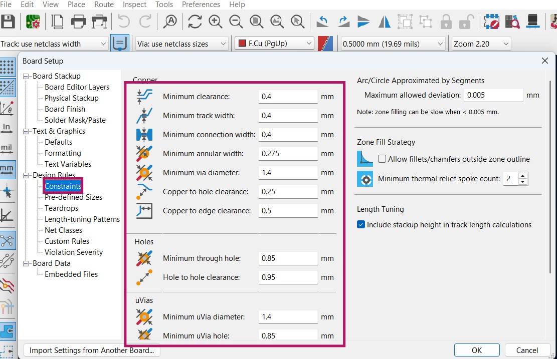
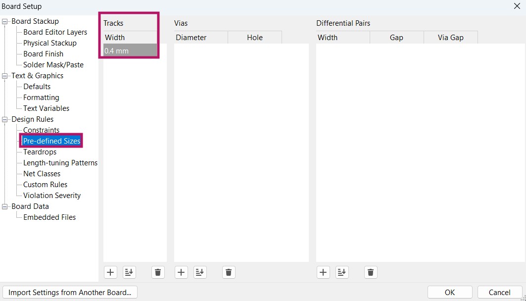
Characterize the design rules for your in-house PCB production process: document the settings for your machine.
Document the workflow for sending a PCB to a boardhouse.
Individual assignments:
Make and test a microcontroller development board that you designed.
Group Assignment Reflection
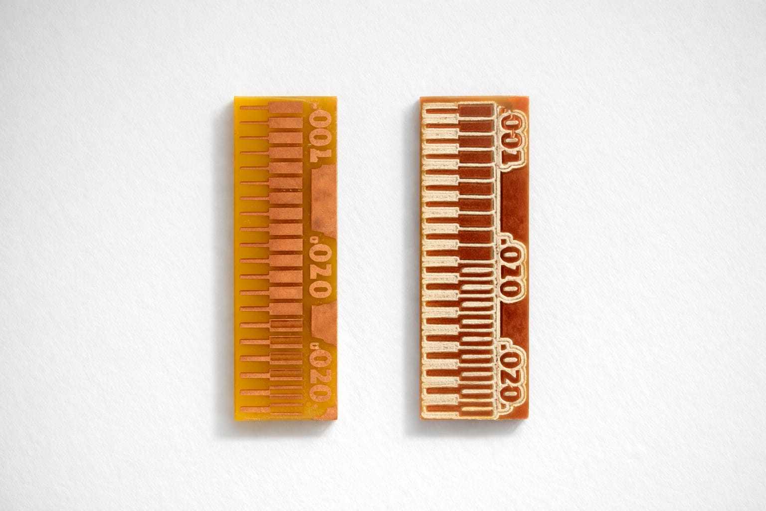
- Tested PCB milling using 0.4 mm end mill and 0.2 mm V-bit
- Observed that V-bit gives better precision for fine traces
- Identified design limits:
- Minimum trace width: 0.3 mm
- Minimum trace spacing: 0.4 mm
- Learned that smaller spacing can cause:
- Trace bridging
- Incomplete isolation
- Understood the importance of:
- Tool selection
- Machine calibration
- Surface flatness
- Explored laser cutting as an alternative fabrication method.
- Helped in understanding practical PCB production constraints for my design
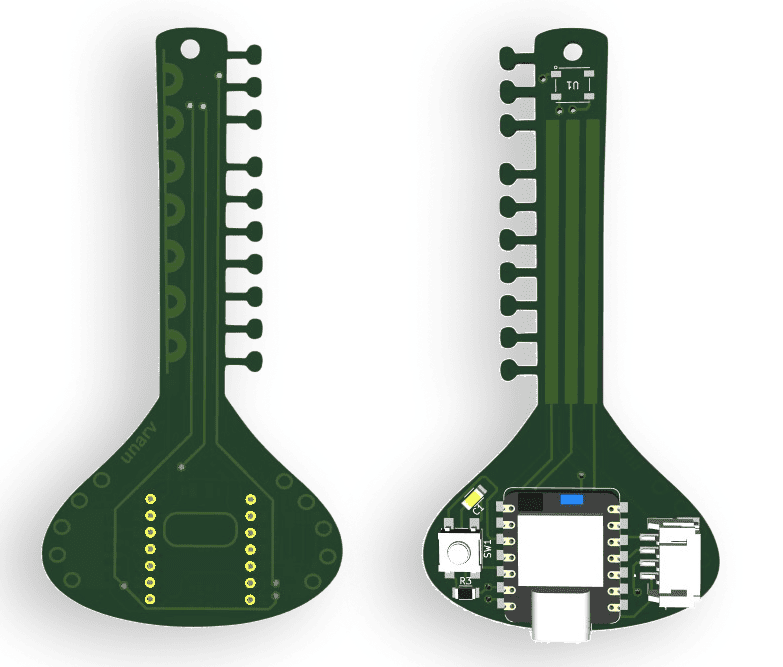
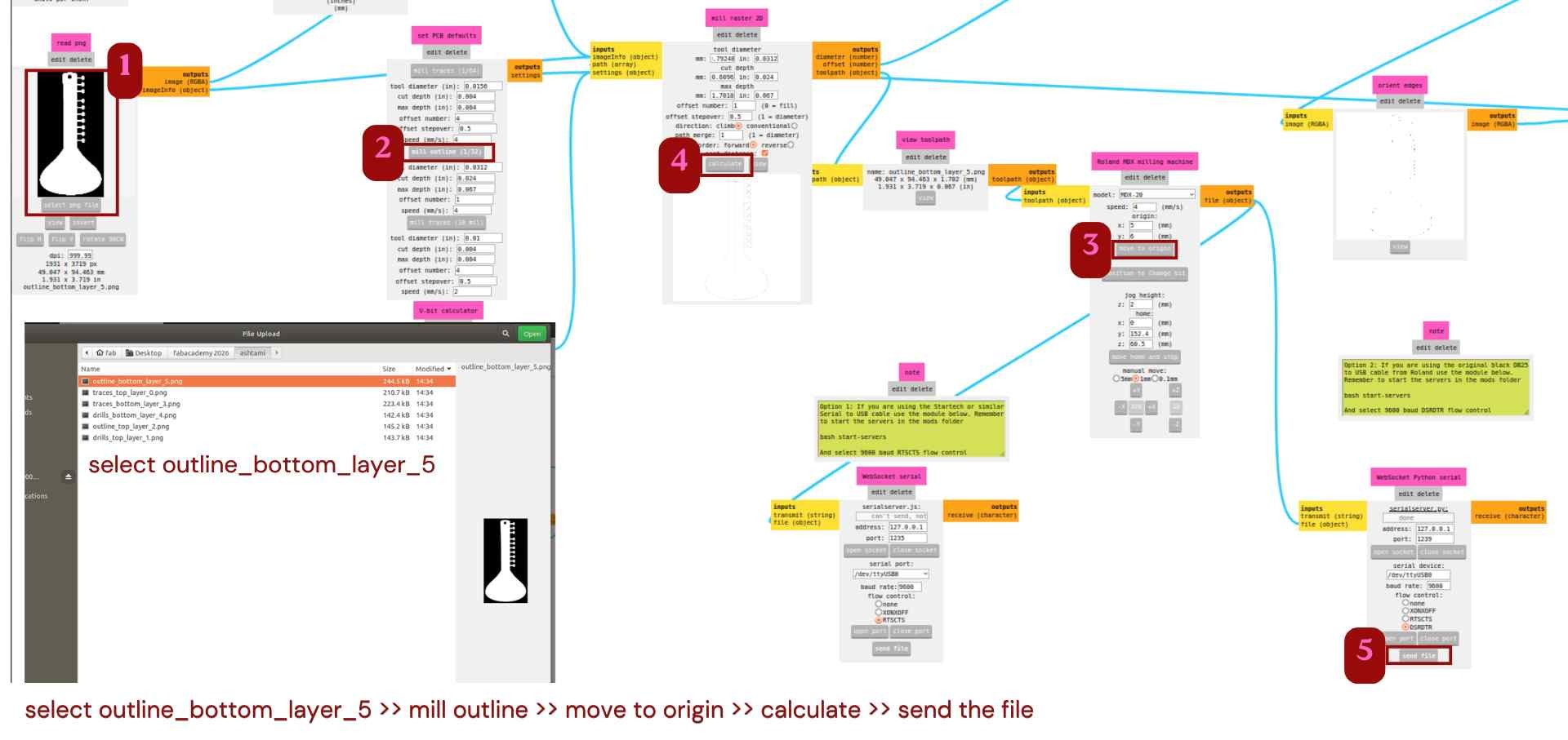
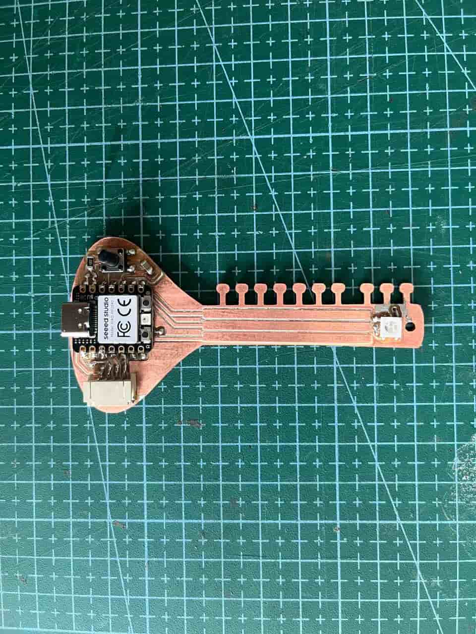
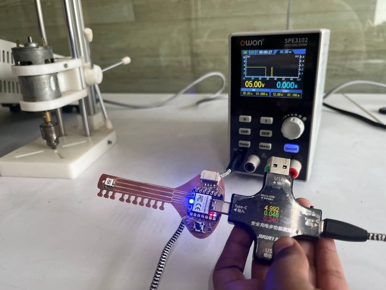
For this week, we are using the PCB designed in KiCad during Electronic Design Week and fabricating it using Modela MDX-20 3D milling machine. I designed a sitar-shaped PCB that includes a Seeed Studio XIAO RP2040, NeoPixel LED, Resistor, Capacitor, a Push Button Switch, and Pin Header.
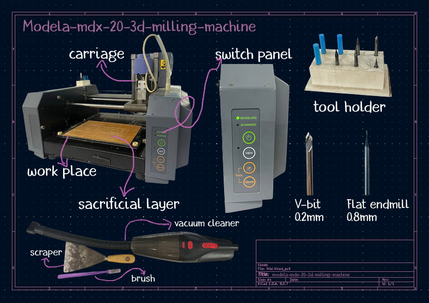
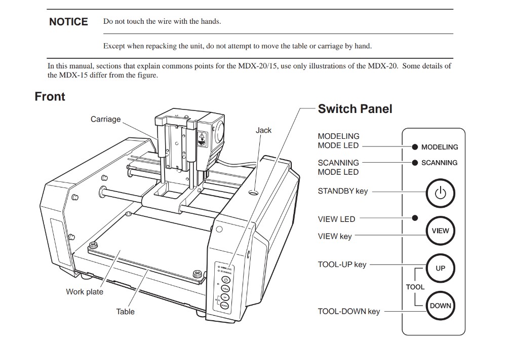
Modela-mdx-20-3d-milling-machine
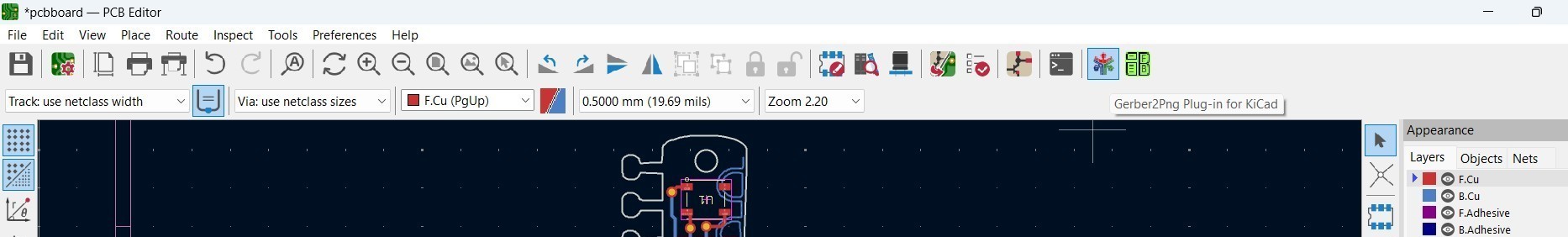
Gerber to Png kicad plugin
A better alternative workflow was created by FabLab Kerala.
They developed a plugin for KiCad that makes the process easier.
Using this plugin in the PCB Editor, the gerber files directly open in the Gerber-to-PNG site.
This eliminates the steps of plotting Gerber files, generating drill files, and manually uploading them to the Gerber-to-PNG website.
To install this plugin in KiCad:
- Open KiCad.
- Go to Plugin and Content Manager.
- Click Install from File.
- Download the ZIP file from github .
- Select the downloaded ZIP file and open it to install the plugin.
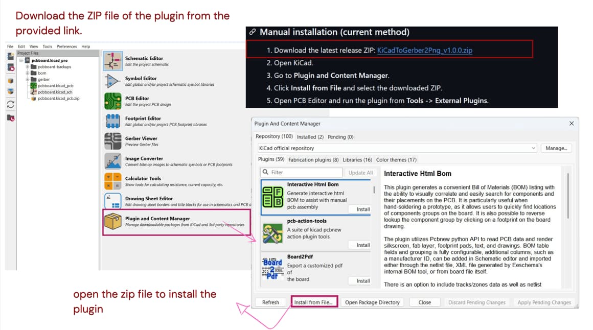
After installation, the plugin will be visible in the PCB Editor. From there, it can be used to directly convert the Gerber files to PNG for the PCB milling workflow.
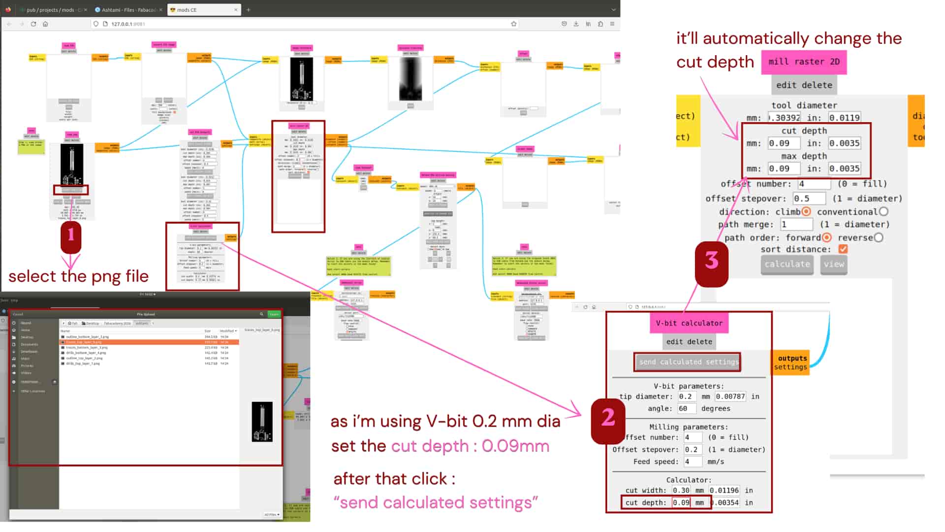
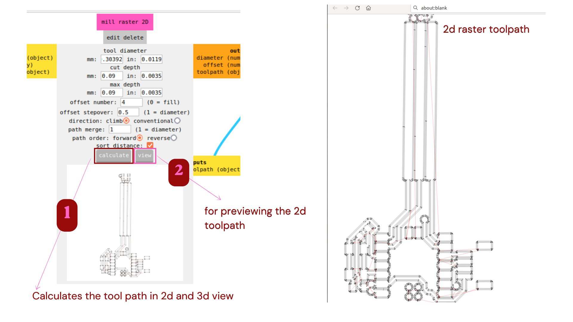
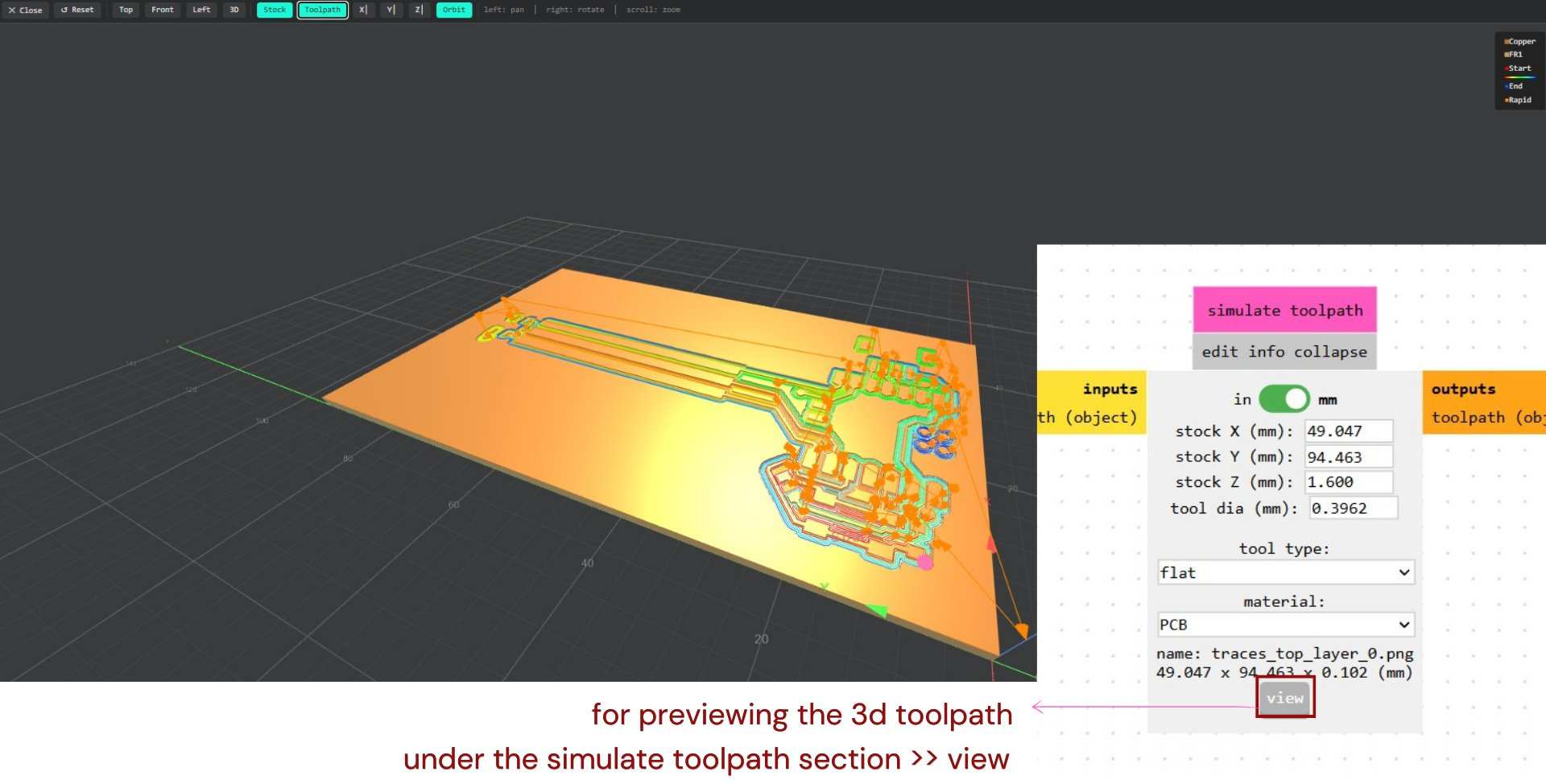
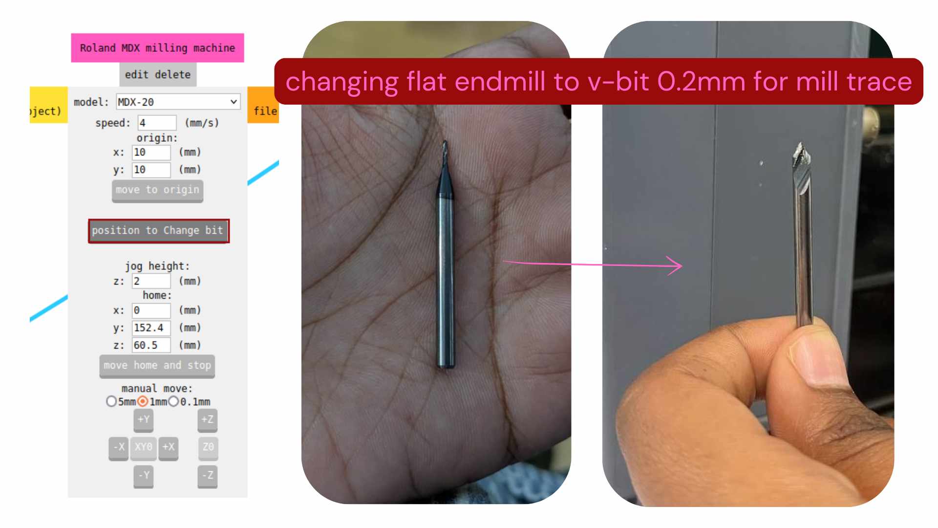
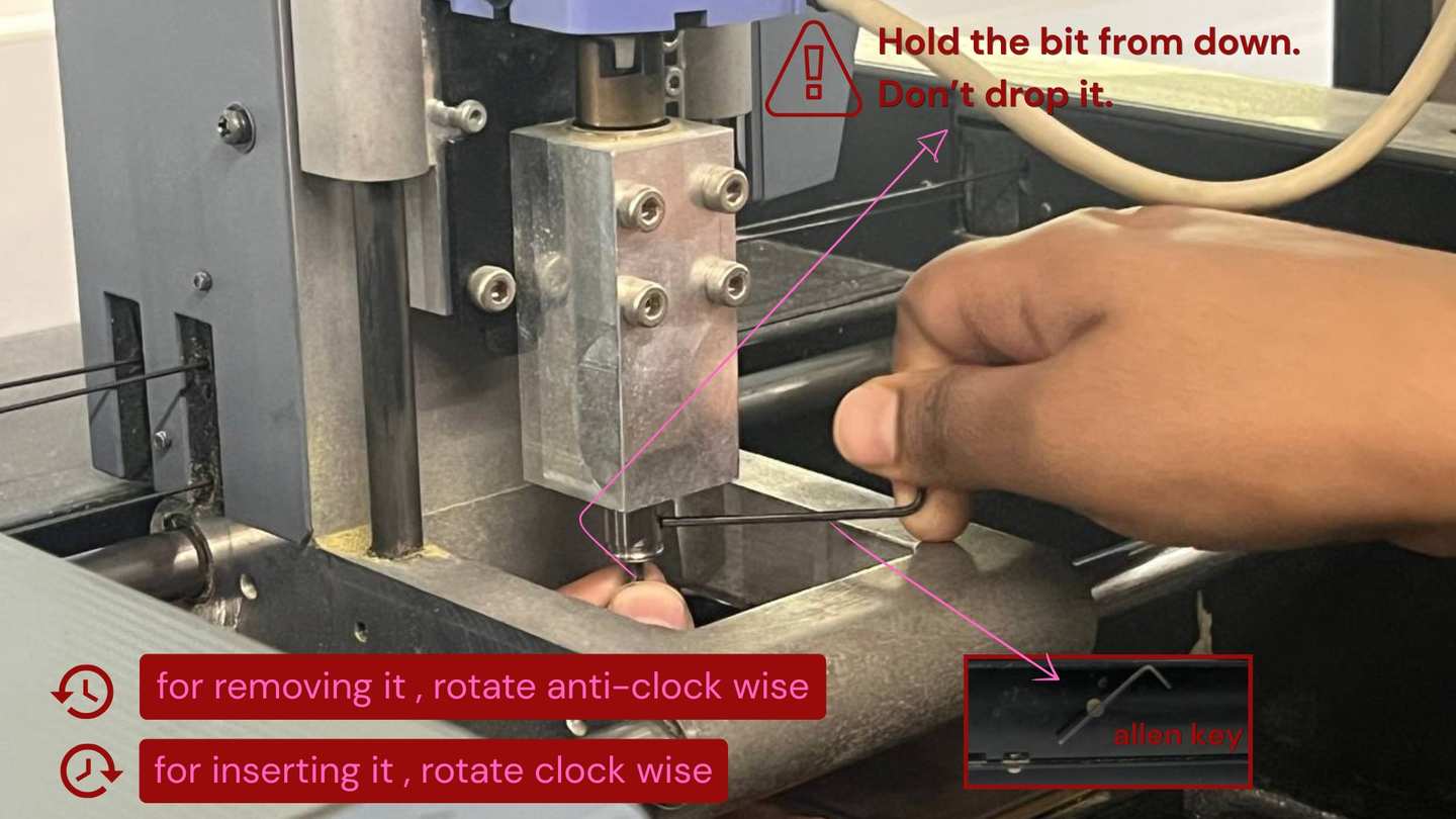
Sitar-PCB Milling Workflow using Roland Modela MDX-20 and MODS CAM
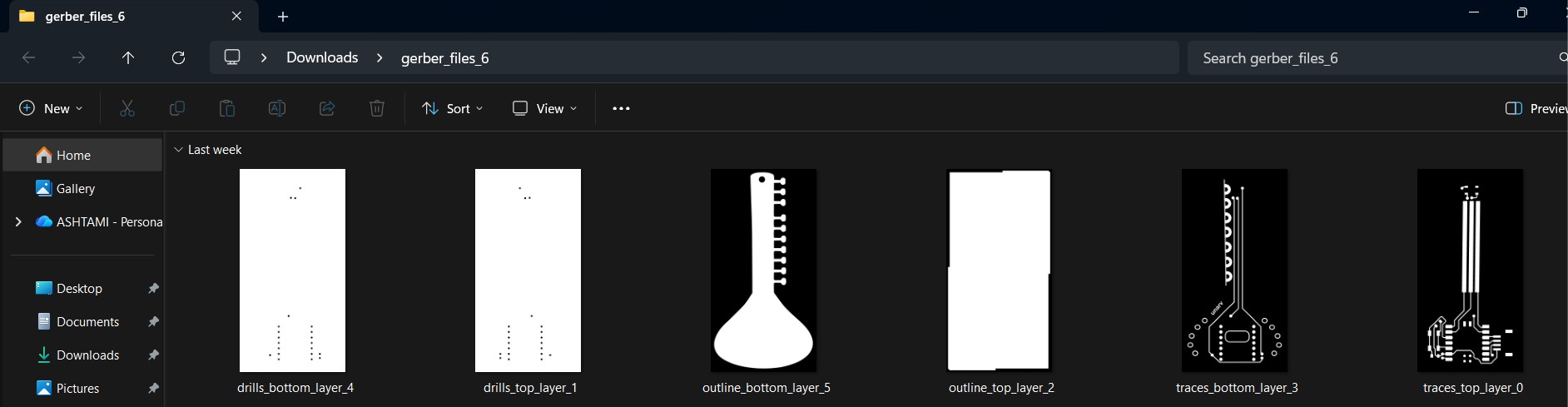
Milling: traces_top_layer_0
Milling: drills_top_layer_1
Milling: traces_top_layer_0, retracing using flat endmill
Milling: outline_top_layer_2
Milling: traces_bottom_layer_3
Milling: drills_bottom_layer_4
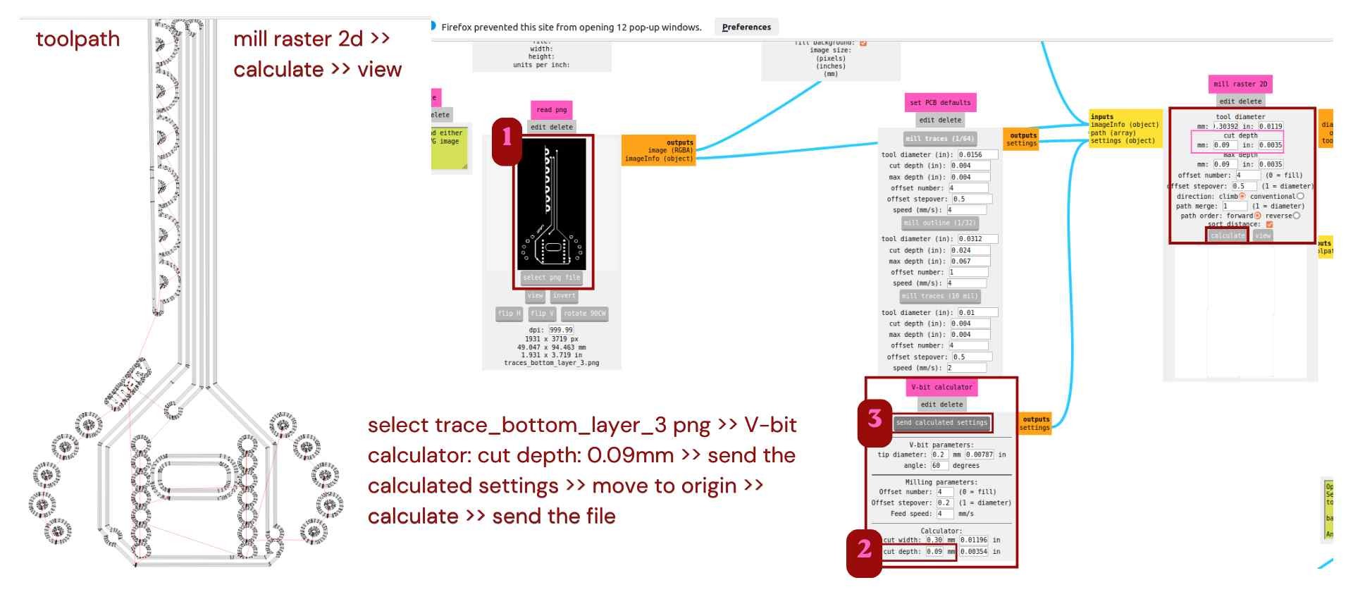
Milling: outline_bottom_layer_5
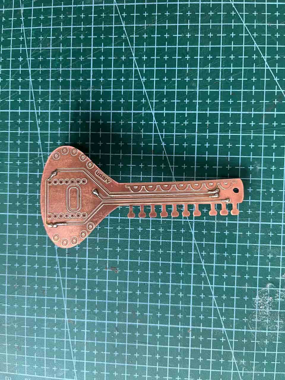
Front side routing
1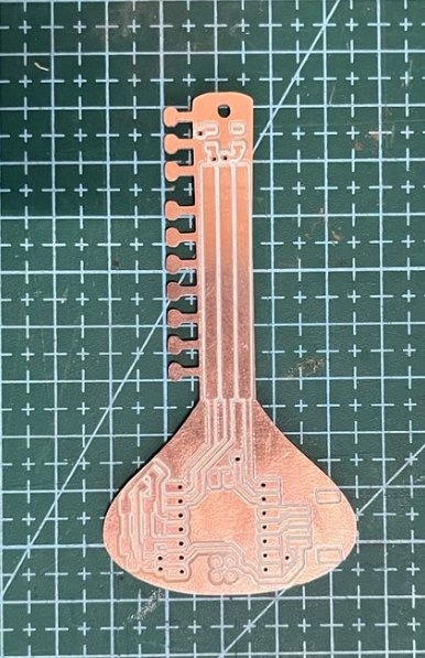
Bottom side routing
2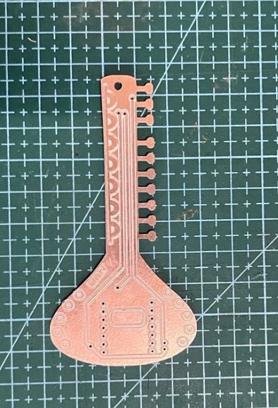
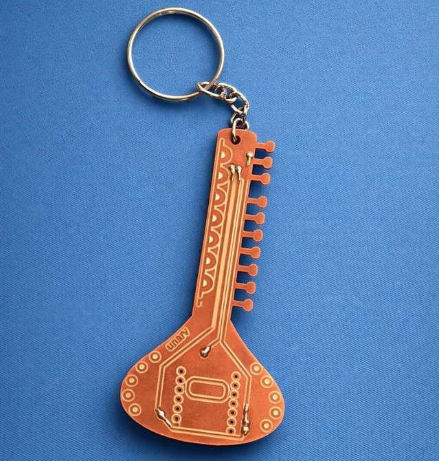
Sitar-shaped Pcb
3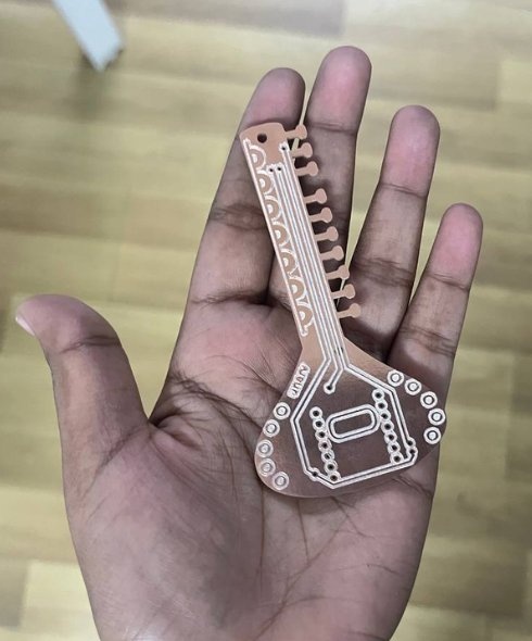
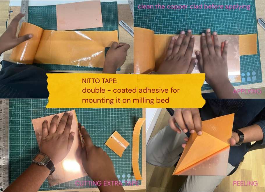
Copper board after cutting
4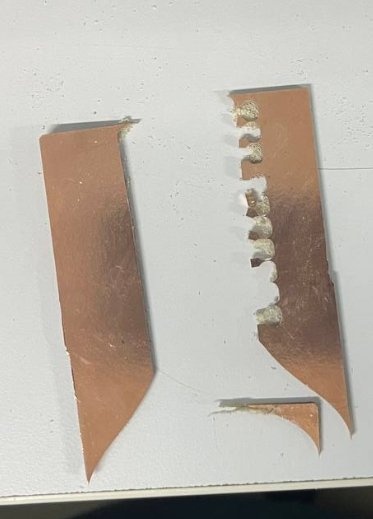
Removing islands
5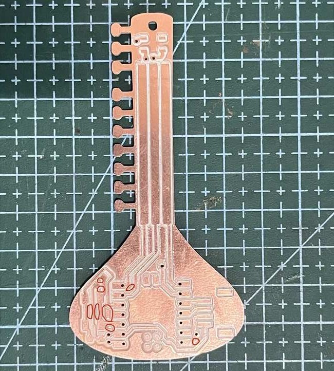
Remove islands to avoid unwanted copper that might short my PCB.
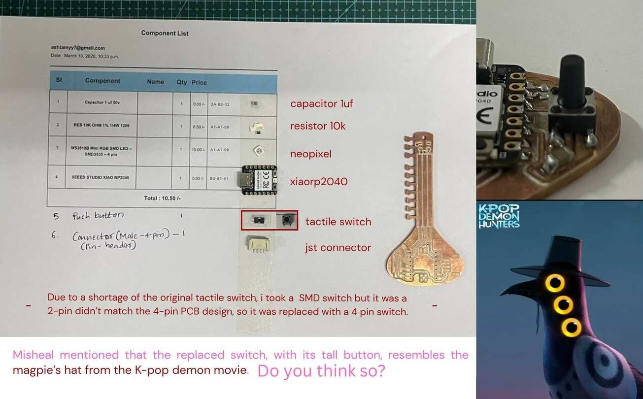
BOM and Material Collection
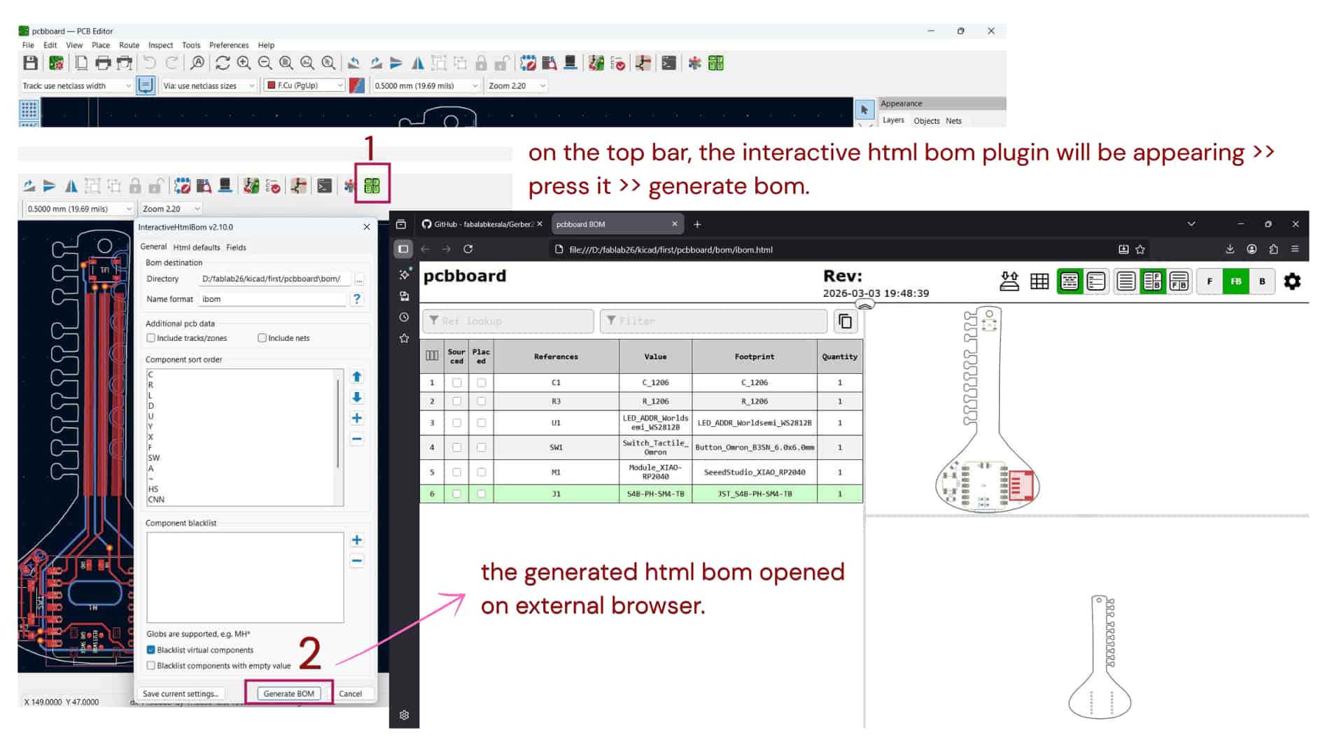
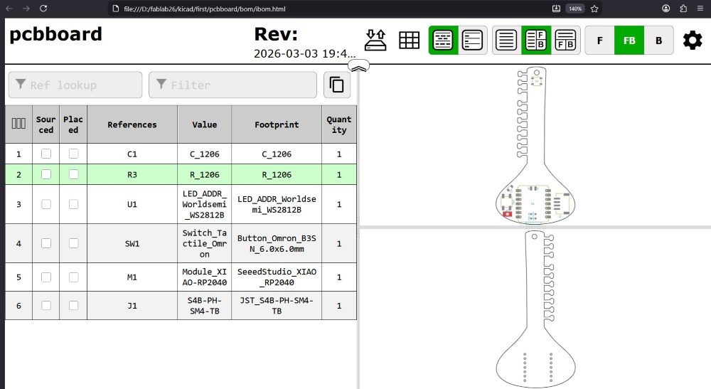
Installed the Interactive HTML BOM plugin.
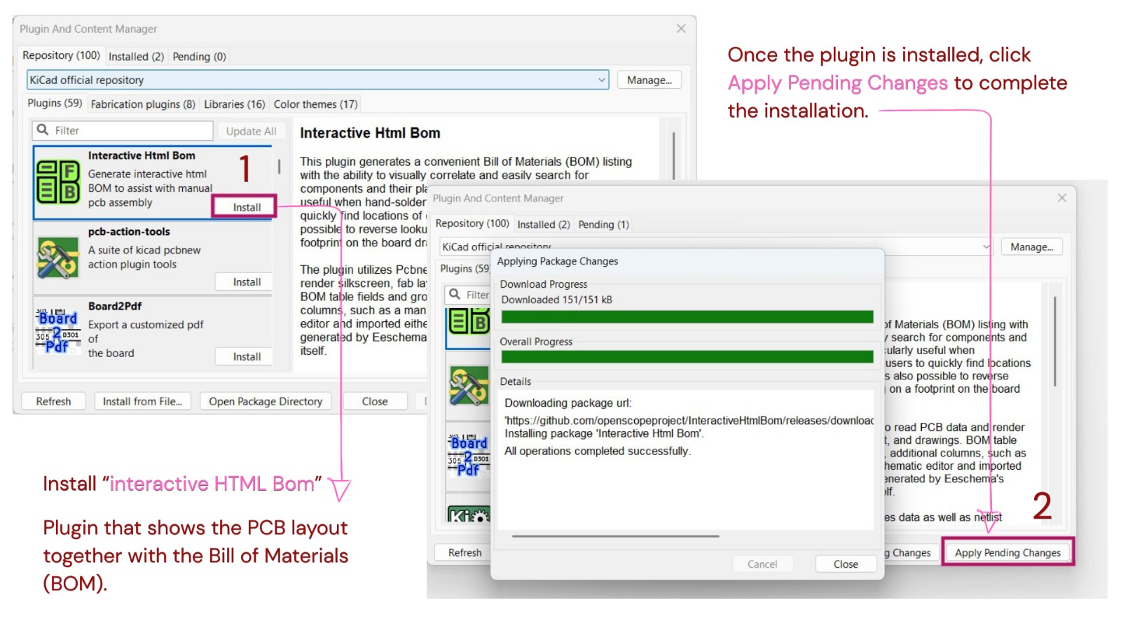
It is a KiCad plugin that shows the PCB layout together with the Bill of Materials (BOM). This helps to easily locate components on the board during assembly. It is helpful during hand-soldering, as you can quickly find where each component is placed and view its details by clicking on it.
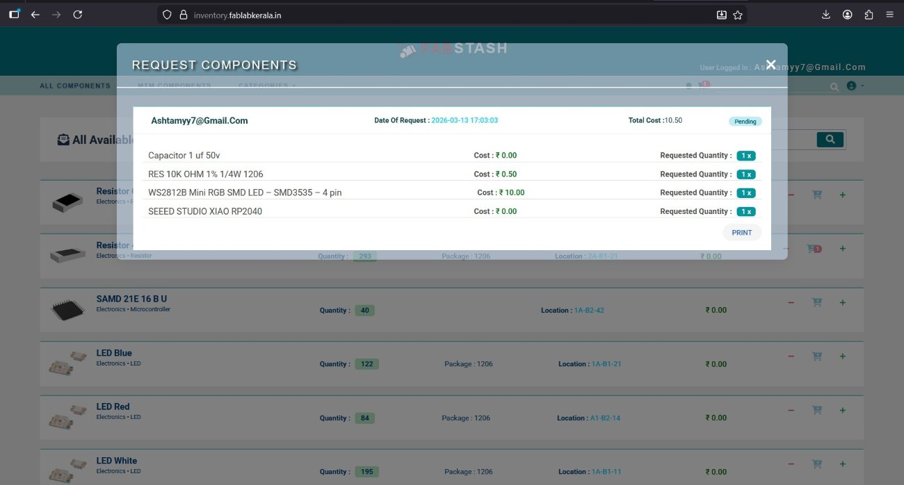
Fabstash inventory
PCB Soldering Process
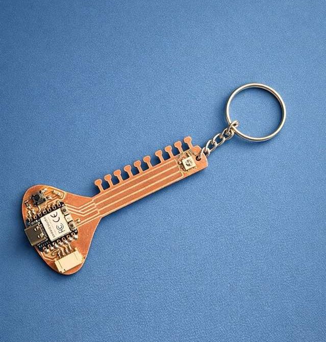
The final PCB shot - Photo credits:Ali
Testing Programming the PCB
              #include
                // This line includes the NeoPixel library so we can control the LED

                #define LED_PIN D5
                // The pin where NeoPixel data line is connected

                #define NUMPIXELS 1
                // Number of NeoPixels are using (i'm using 1 LED)

                Adafruit_NeoPixel pixels(NUMPIXELS, LED_PIN, NEO_GRB + NEO_KHZ800);
                // Named NeoPixel as "pixels"
                // NUMPIXELS : how many LEDs
                // LED_PIN : which pin is used
                // NEO_GRB : color format (order of colors)
                // NEO_KHZ800 : communication speed

                void setup() {
                  pixels.begin();
                  // Initializes the NeoPixel library (must be called once)
                }

                void loop() {

                  pixels.setPixelColor(0, pixels.Color(255,0,0));
                  // Set LED at index 0 to RED color (R=255, G=0, B=0)

                  pixels.show();
                  // Sends the color data to the LED (without this, nothing changes)

                  delay(1000);
                  // Wait for 1 second (1000 milliseconds)

                  pixels.setPixelColor(0, pixels.Color(0,255,0));
                  // Change LED to GREEN (R=0, G=255, B=0)

                  pixels.show();
                  // Update the LED with new color

                  delay(1000);
                  // Wait for 1 second

                  pixels.setPixelColor(0, pixels.Color(0,0,255));
                  // Change LED to BLUE (R=0, G=0, B=255)

                  pixels.show();
                  // Update the LED

                  delay(1000);
                  // Wait for 1 second
                }
Chatgpt_AI Prompt Used
                I designed a sitar-shaped PCB using a XIAO RP2040. It includes a NeoPixel (connected to D5), a push button, resistor, capacitor, JST male connector, and touch pads.
                First, I want to test and control the NeoPixel. After that, I want to play music when someone touches the pads.