Electronics Design
Task:-
Group assignment:
Use the test equipment in your lab to observe the operation of a microcontroller circuit board
(as a minimum, you should demonstrate the use of a logic analyzer)
Individual assignments:
Use an EDA tool to design a development board that uses parts from the inventory to
interact and communicate with an embedded microcontroller
Overview of Group Assignment
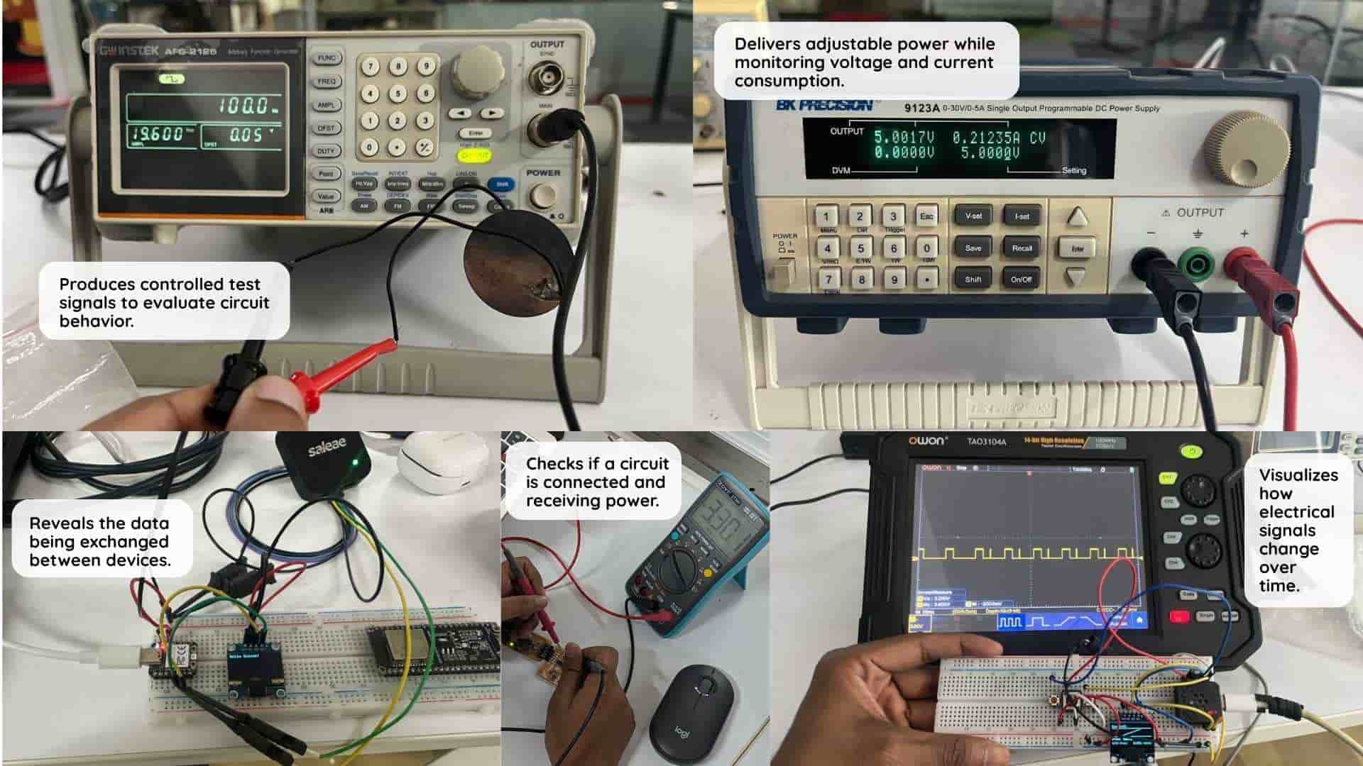
In this group assignment, we used the electronic test equipment available in our lab to observe, measure, and analyze the operation of an embedded microcontroller system. By using different instruments, we learned how to verify power, visualize electrical signals, and debug communication between electronic devices.
The Seeed Studio XIAO RP2040, a development board based on the RP2040 chip, was programmed to generate test signals and communication data that were analyzed using the lab equipment.
Source: Mishael's week 6 documentation
Digital Multimeter (DMM)
Purpose: Measures voltage, resistance, and continuity.
We used it to: Check circuit continuity before powering the board and verify the correct supply voltage after powering it.
Outcome: Confirmed proper connections and correct voltage levels.
Bench Power Supply
Purpose: Provides adjustable and protected DC power.
We used it to: Safely power the circuit and observe current consumption while testing different operating conditions.
Outcome: Measured stable power delivery and monitored current draw.
Oscilloscope (OWON TAO3104A)
Purpose: Displays electrical signals as waveforms.
We used it to: Observe the signals generated by the XIAO RP2040.
Outcome: Successfully viewed and analyzed the output waveforms.
Logic Analyzer (Saleae Logic 8)
Purpose: Captures and interprets digital communication.
We used it to: Analyze UART and I2C communication sent by the XIAO RP2040.
Outcome: Successfully decoded the communication data.
For detailed information, refer to: Electronic Design Week Group Assignment
Individual Assisgnments
KiCad
KiCad is a free EDA (Electronic Design Automation) tool where you first draw your circuit (schematic), then design the board (PCB - Printed Circuit Boards ), and finally preview it in 3D before manufacturing.
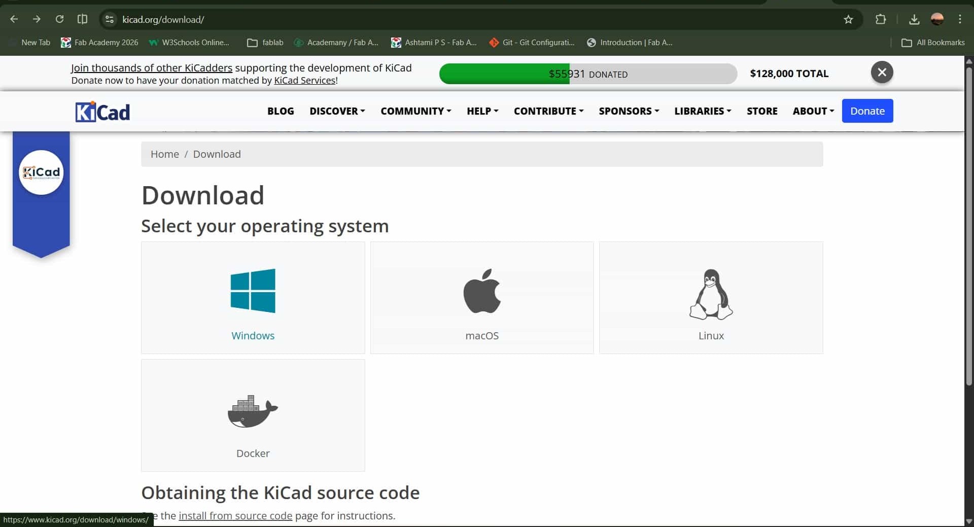
Installing kiCadI downloaded the Windows version of KiCad. While downloading, there are continent or region-based options available. All versions are the same — only the download server location changes. Since I am in Asia, I selected the Asia server, and the file is 1GB, quite large. After downloading, I installed KiCad on my PC by running the setup file and following the installation steps.

Introduction to Kicad interface
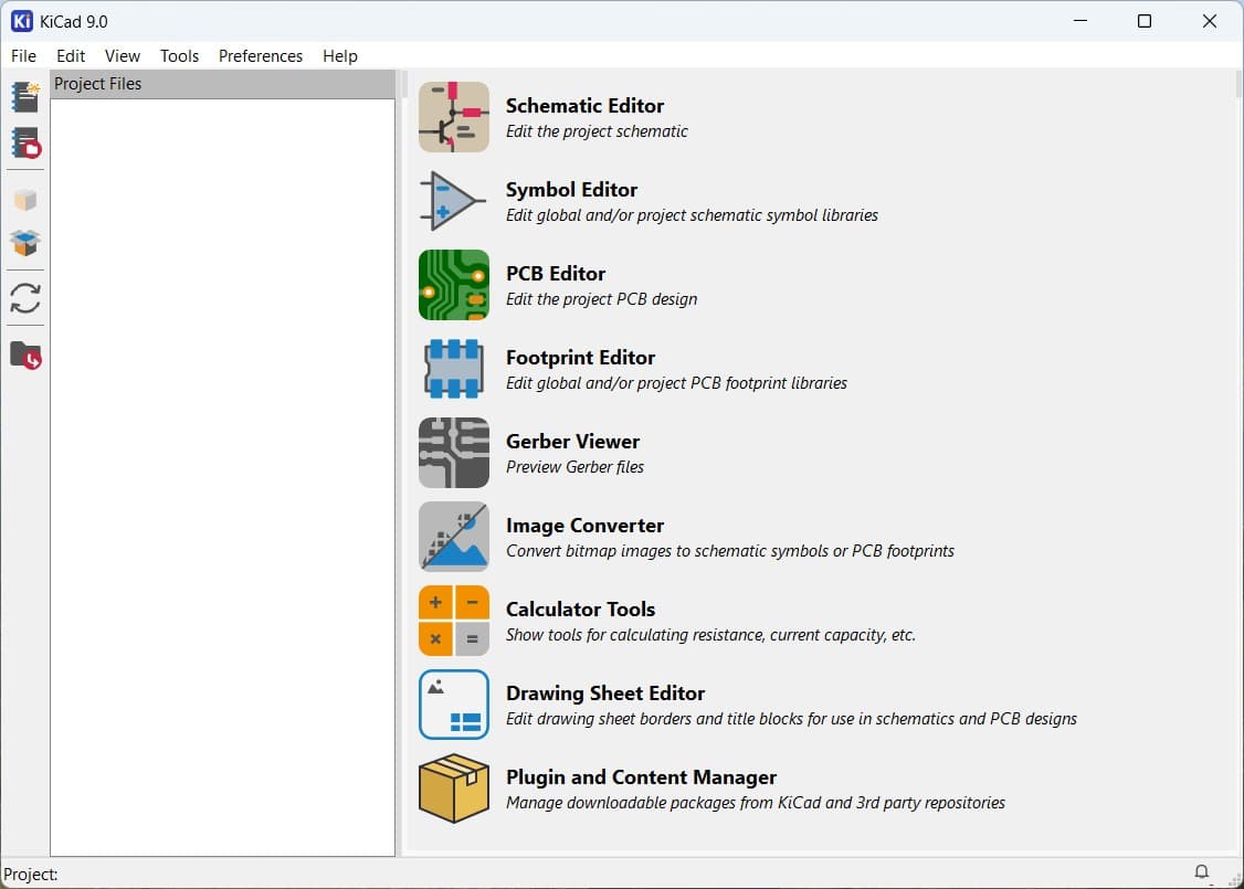
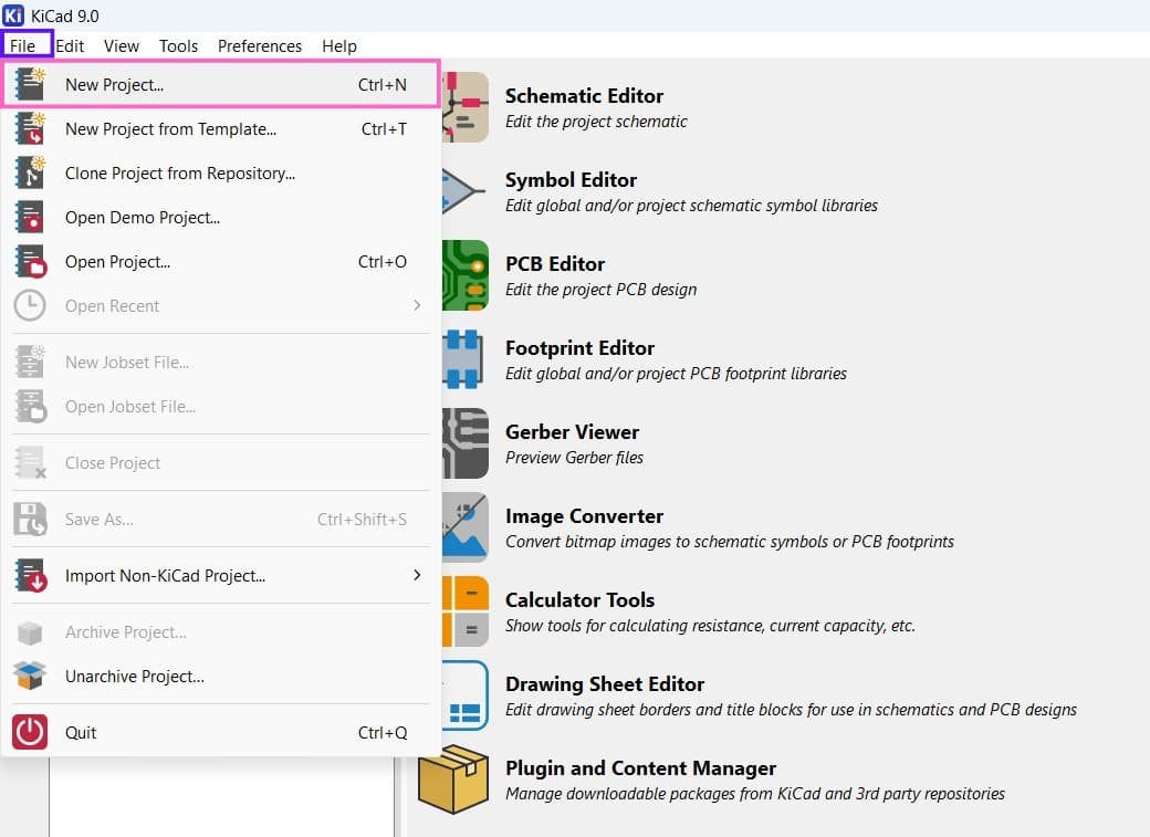
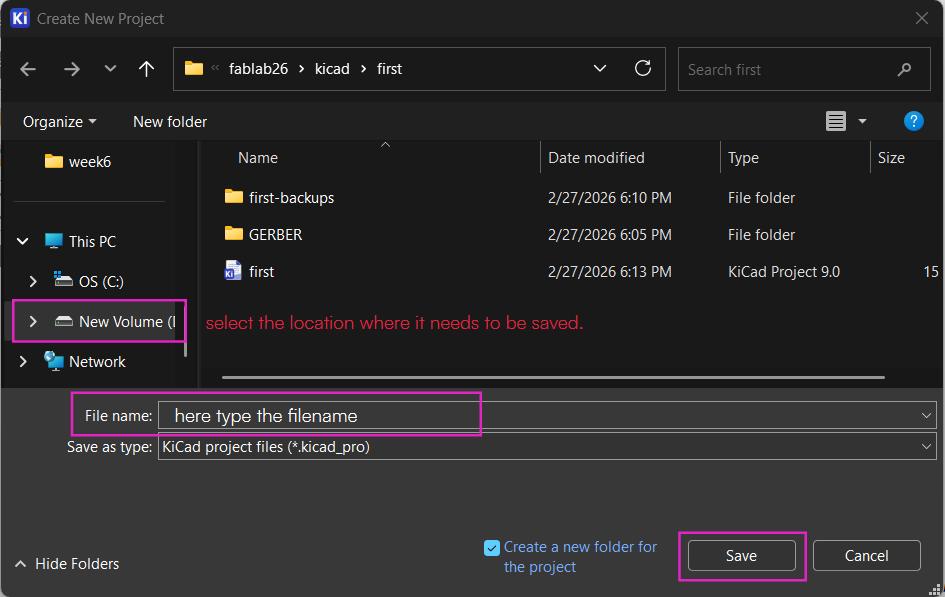
For creating new project: Files >> New Project
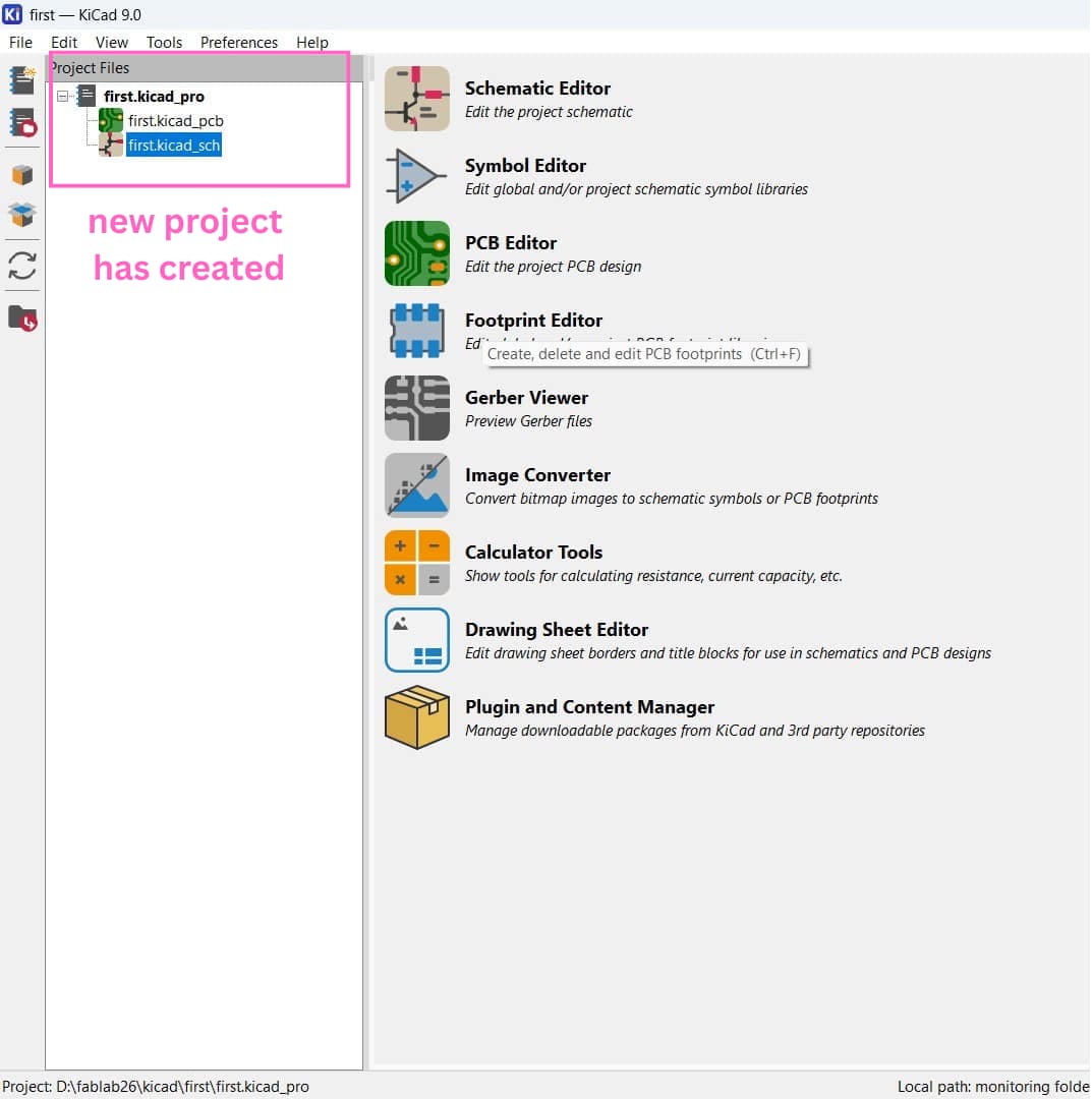
When you create a new project in KiCad, it automatically generates the project folder along with the schematic file and the PCB file.
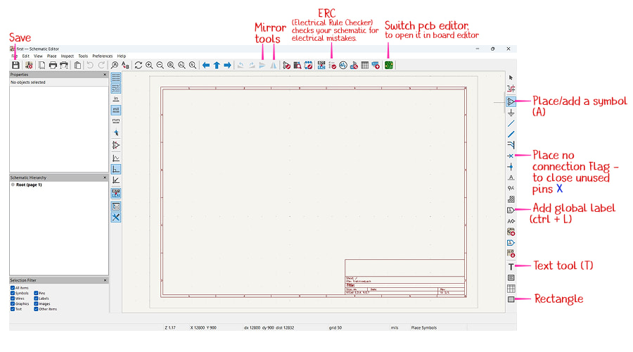
Schematic Editor interface
A schematic is used to draw and plan an electronic circuit before creating the actual PCB.
It shows components using standard electronic symbols and uses wires (lines) to connect them,
representing how electricity flows in the circuit.
In simple terms, a schematic is the blueprint of your electronics project,
helping you clearly organize connections and avoid mistakes before designing the physical PCB.
Shortcut Keys for Schematic Editor
| Shortcut keys | Purpose |
|---|---|
| A | Place symbols(add) |
| M | For moving symbols |
| R | Rotate a symbols, press 'R' again to rotate in different direction |
| Y | Mirror a symbol vertically, top-bottom |
| X | Mirror a symbol horizontally, left-right |
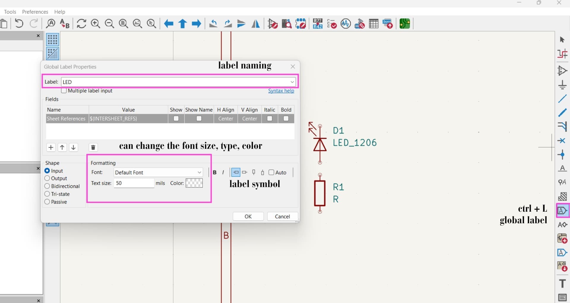
| Ctrl + L | For placing or giving a global label to symbols |
| E | Edit properties |
| Q | Place no connection Flag |
| G | For dragging a symbol with the connected wire |
| Delete | Remove a symbol |
| W | Start a wire |
| ~ | For checking symbol connection |
The PCB Editor in KiCad is used to design the physical layout of your circuit board.
After creating the schematic, you import it into the PCB Editor, where you place the components,
arrange them properly, and draw copper tracks to connect them.
The right toolbar contains tools to add footprints, draw tracks, add text,
and create board outlines, while the top toolbar allows you to rotate, mirror components,
edit footprints, run checks, import/update from the schematic editor and open the 3D viewer.
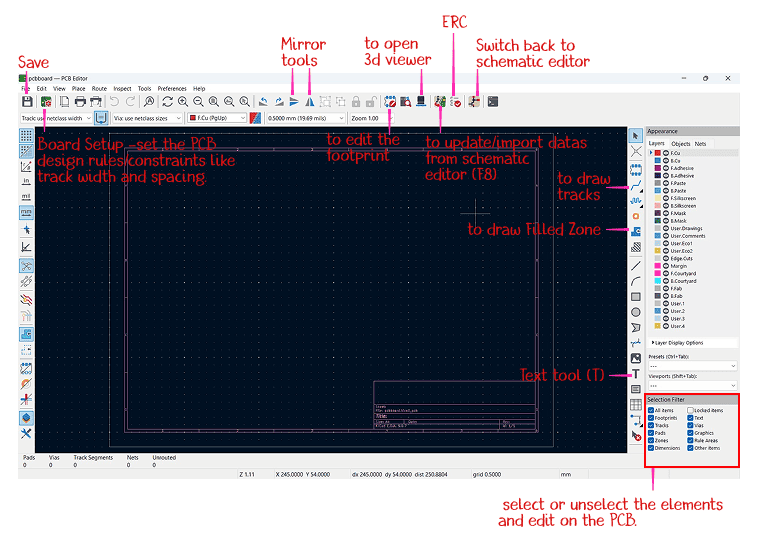
Shortcut Keys for Schematic Editor
| Shortcut keys | Purpose |
|---|---|
| X | To draw track |
| Ctrl+Shift+X | To draw fill zone |
| A | Place footprint |
| Alt+3 | To view pcb in 3d viewer |
| F8 | Update the pcb from schematic editor |
Installation of Fablib
FabLib is a KiCad library made for Fab Academy that includes most components from the Fab Lab inventory, so their symbols and footprints can be easily added, ensuring a 1:1 match for PCB designing.
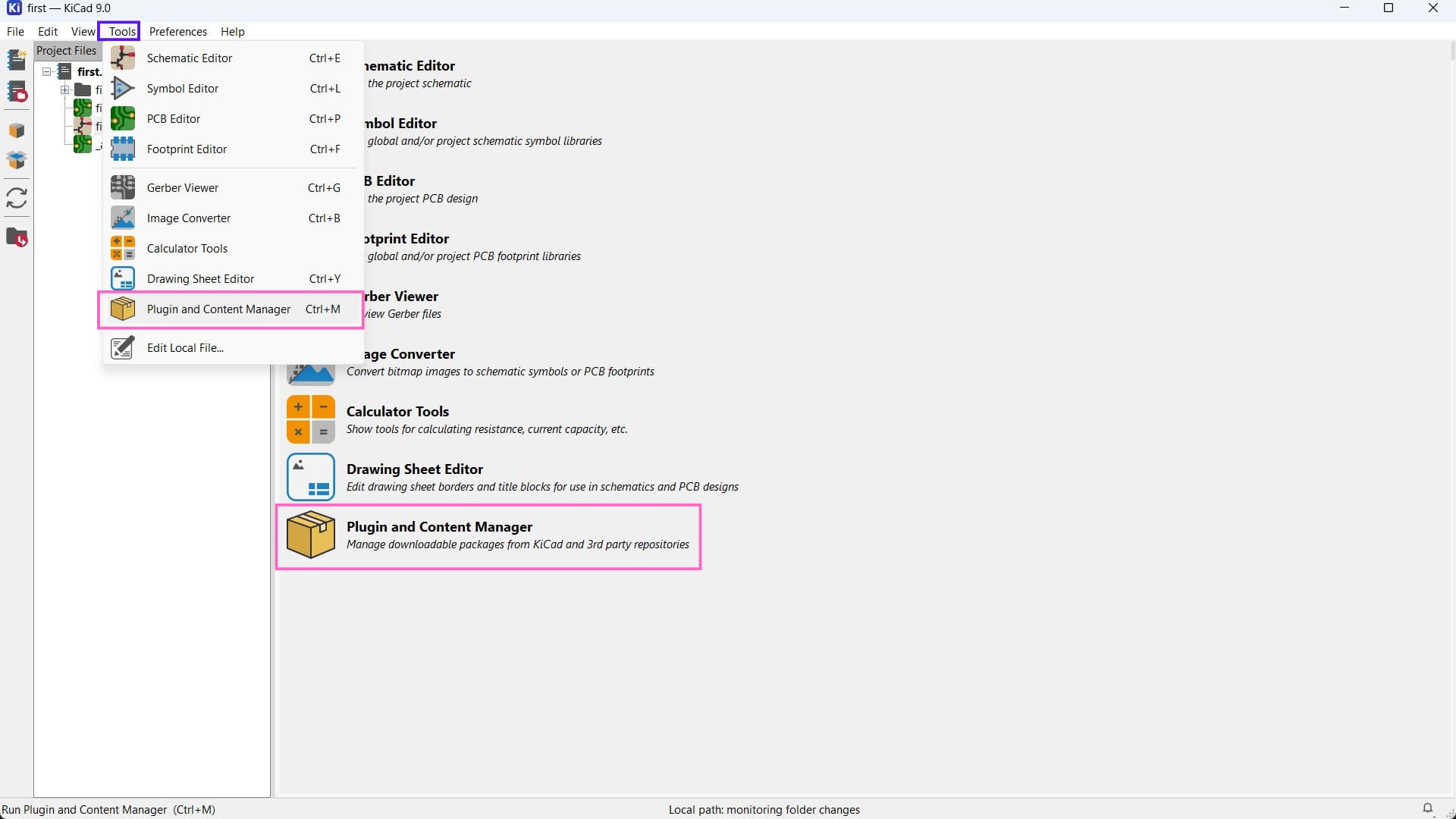
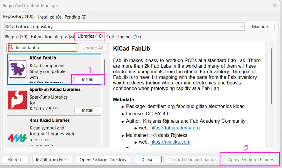
Go to Tools >> Plugin and Content Manager (or press Ctrl + M) >> Open the Libraries tab >> Search for KiCad FabLib >> Click Install >> Click Apply Pending Changes
From Schematic to PCB Layout and 3D View
Our instructor introduced us to KiCad and explained what can be done using the software.
To understand the workflow, we created a simple project starting from circuit design,
then moved to the PCB layout, and finally viewed it in 3D view.
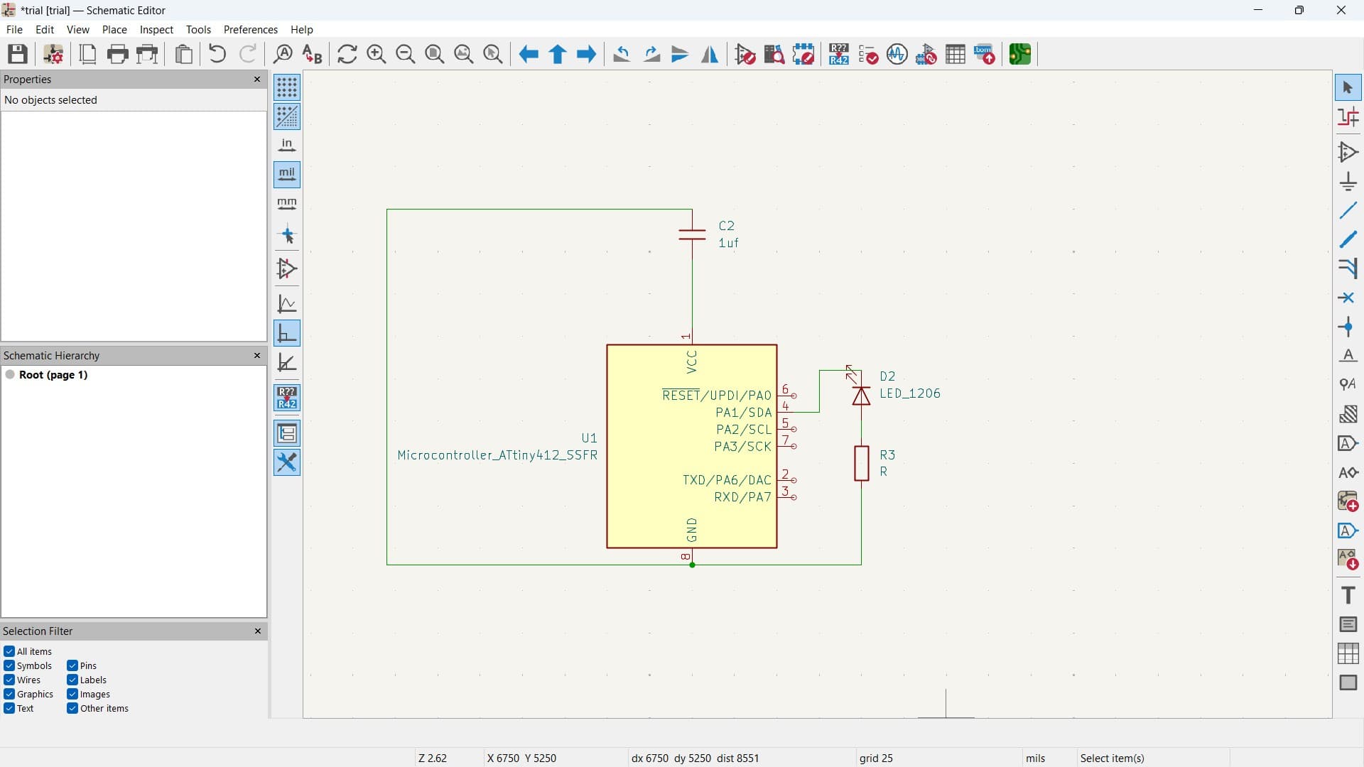
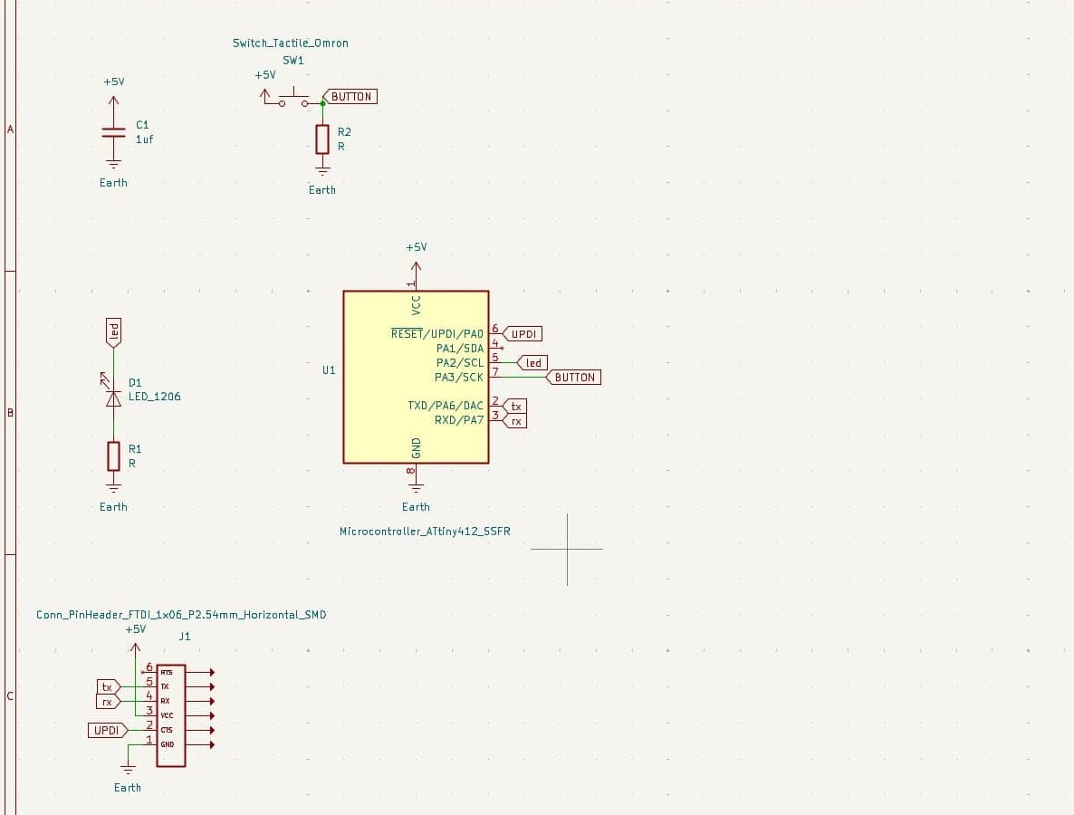
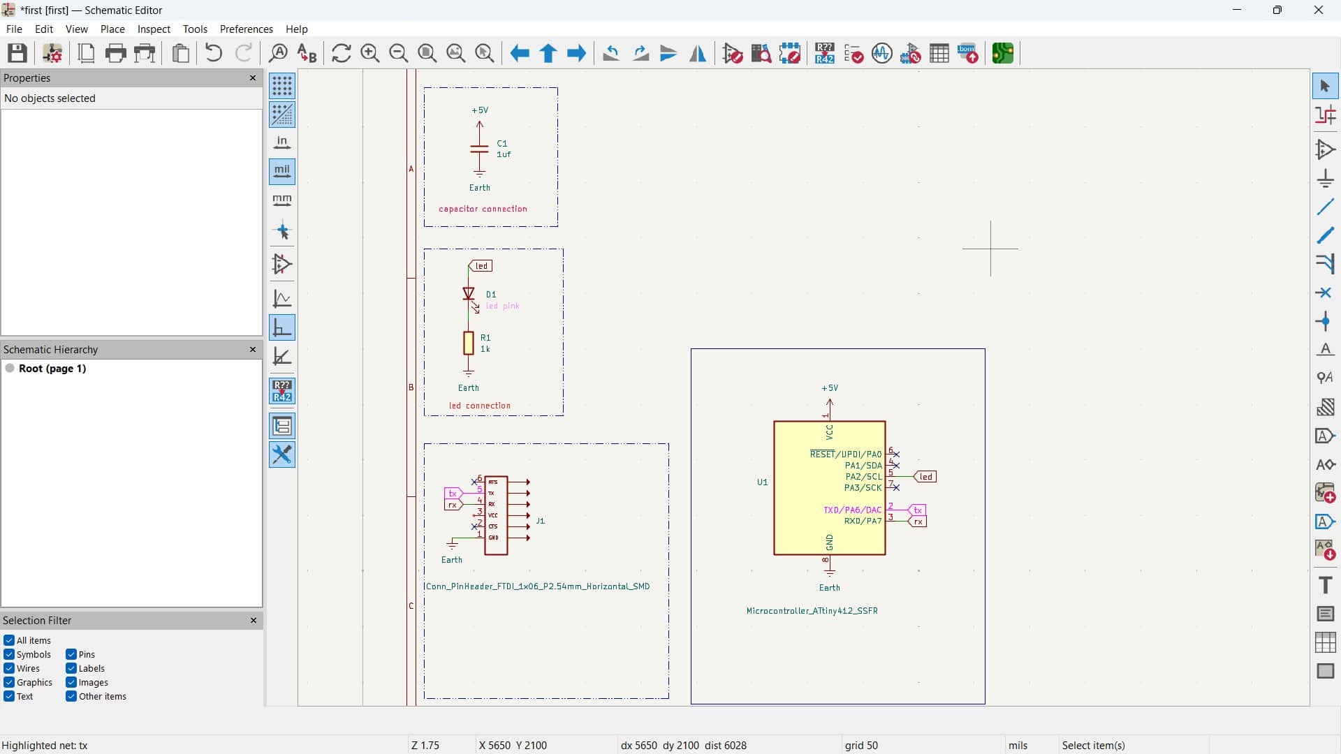
For this circuit, we used ATtiny412, LEDs, two resistors, an FTDI header, and a capacitor.
Here is the workflow:
Creating the Circuit in the Schematic Editor
Once you create the project file, open the schematic editor.
Adding a symbol
Then press A on the keyboard or select Place Symbol from the right toolbar.
A dialog box will open where you can search for components.
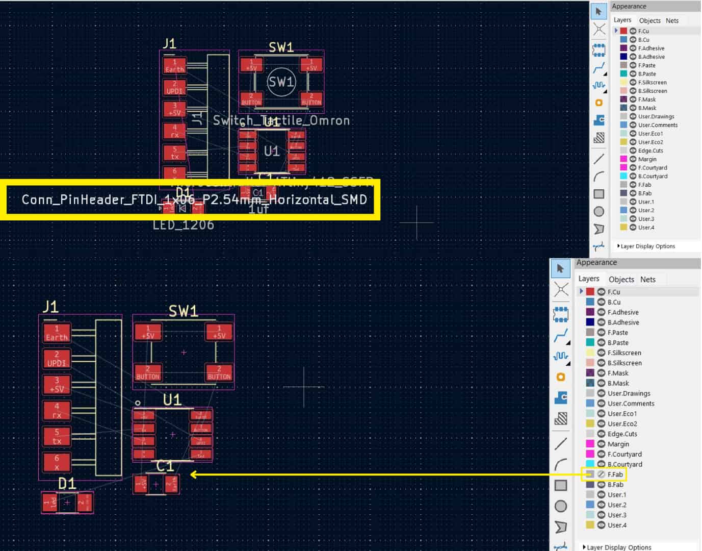
Search for attiny412 fab and select it. On the right side, you will see the symbol and footprint.
Make sure the component has a footprint assigned, because this footprint will be used later when switching to the PCB editor.
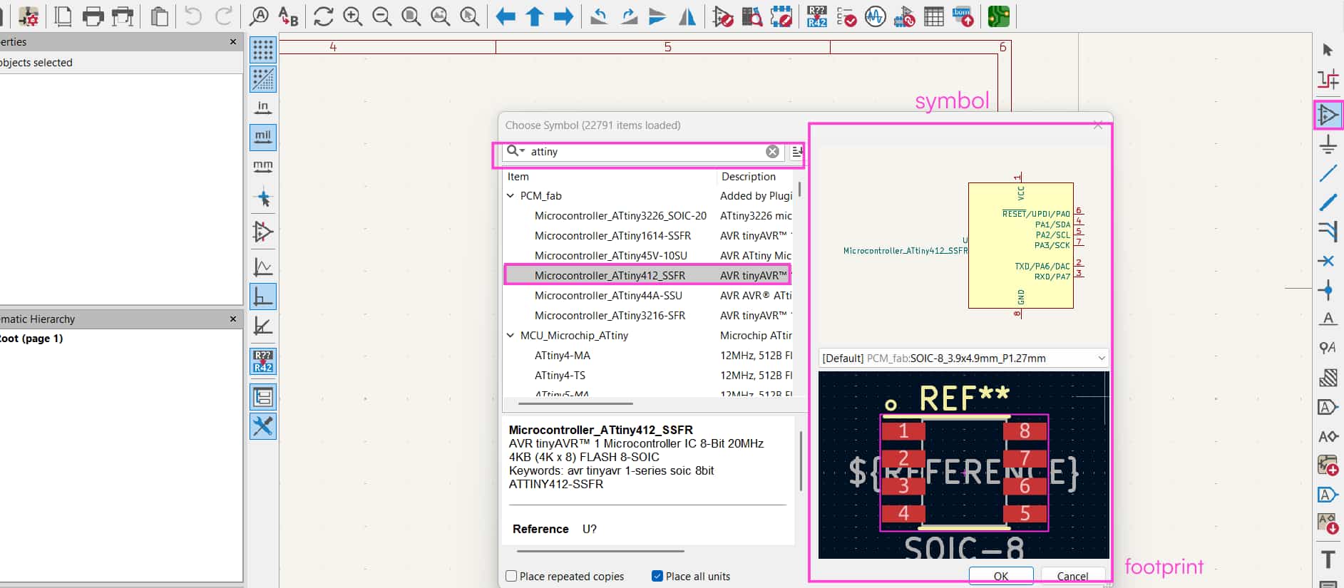
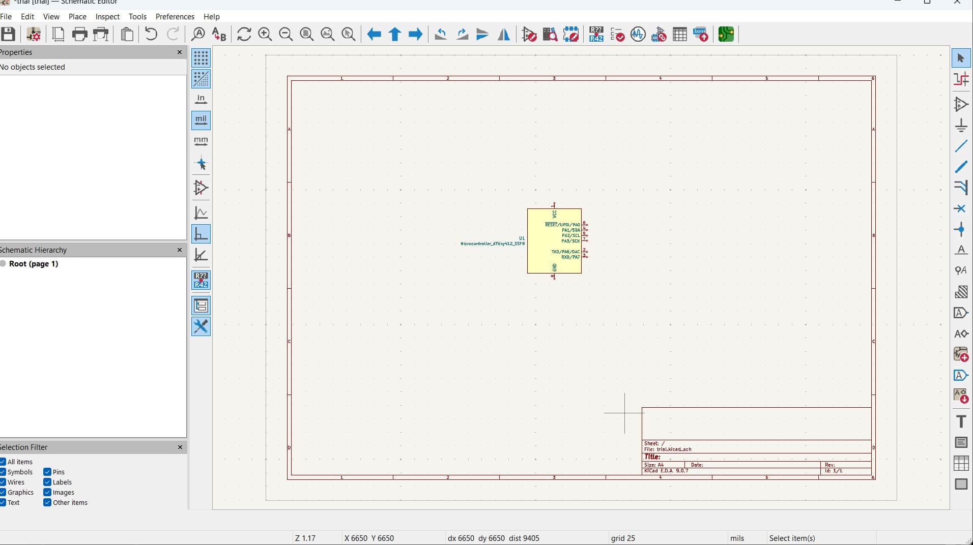
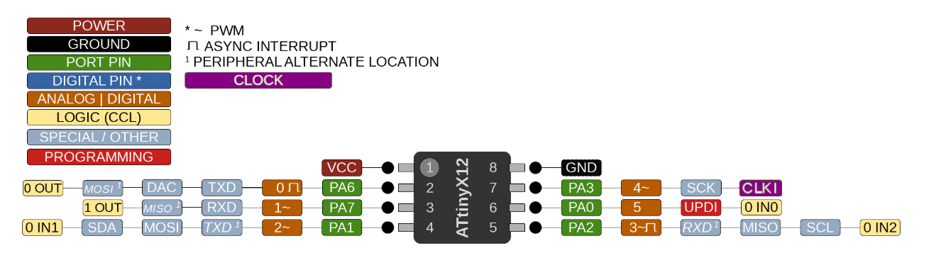
Attiny412: Microcontroller
Components and their symbols used:
Microcontroller
Qty.1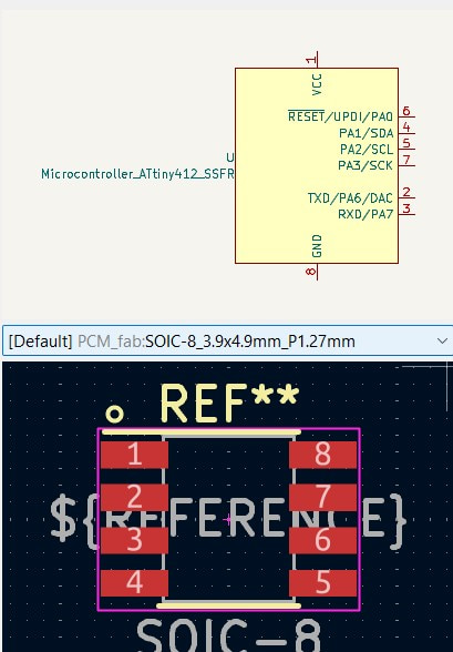
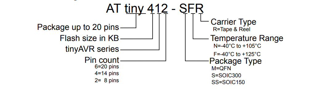
ATtiny412
LED
Qty.1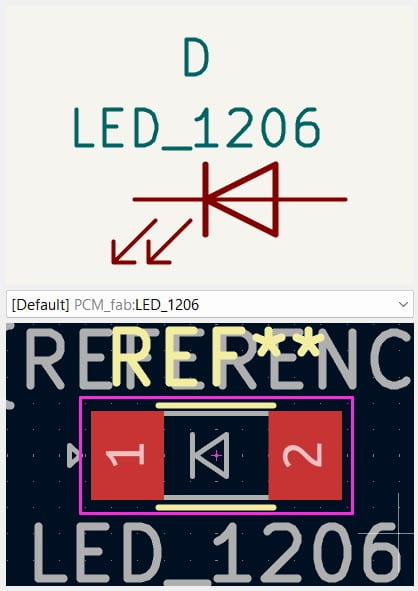
Led_1206
Resistor
Qty.2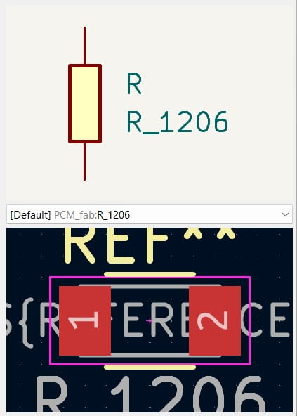
R_1206
Capacitor
Qty.1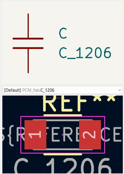
C_1206
Push BUtton
Qty.1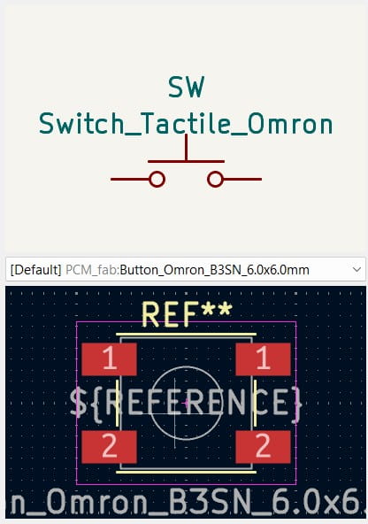
Switch_Tactile_Omron
FTDI
Qty.1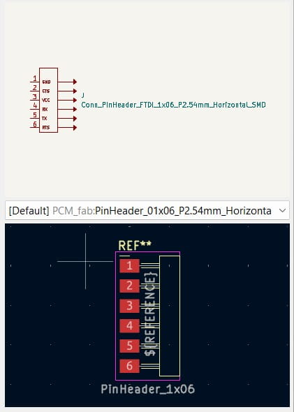
Conn_PinHeader_
FTDI_1x06_P2.54mm_
Horizontal_SMD
Methods of Connecting Components: Wire connection and Global label
There are two ways to connect component symbols in the schematic:
either by drawing wires between the components or by using labels,
such as global labels, to connect them logically. It also allows to use both methods together in the same schematic editor.
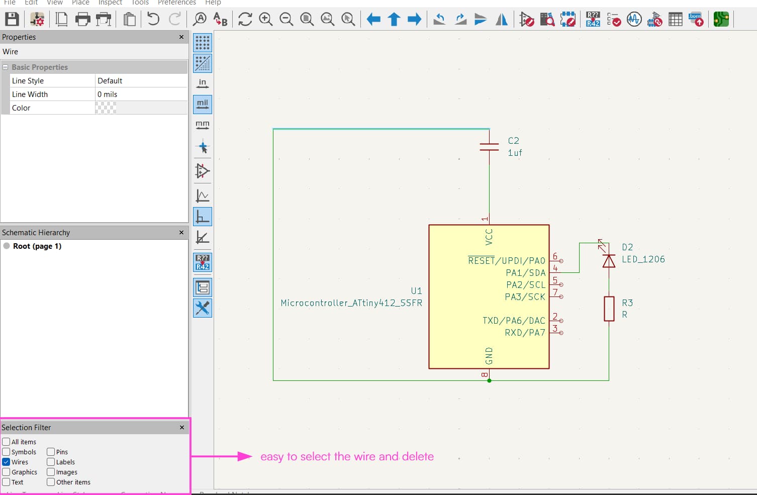
1. Wire Connection:
Components are connected by drawing wires directly between their pins,
which visually shows how each component is linked in the circuit.
At the bottom, there is an option called Selection Filter. By ticking just the "Wires", and unselecting others; only the wires in the schematic can be selected. This allows wires to be selected and deleted easily without accidentally selecting symbols or other elements, no mess of clicking on each wire individually.
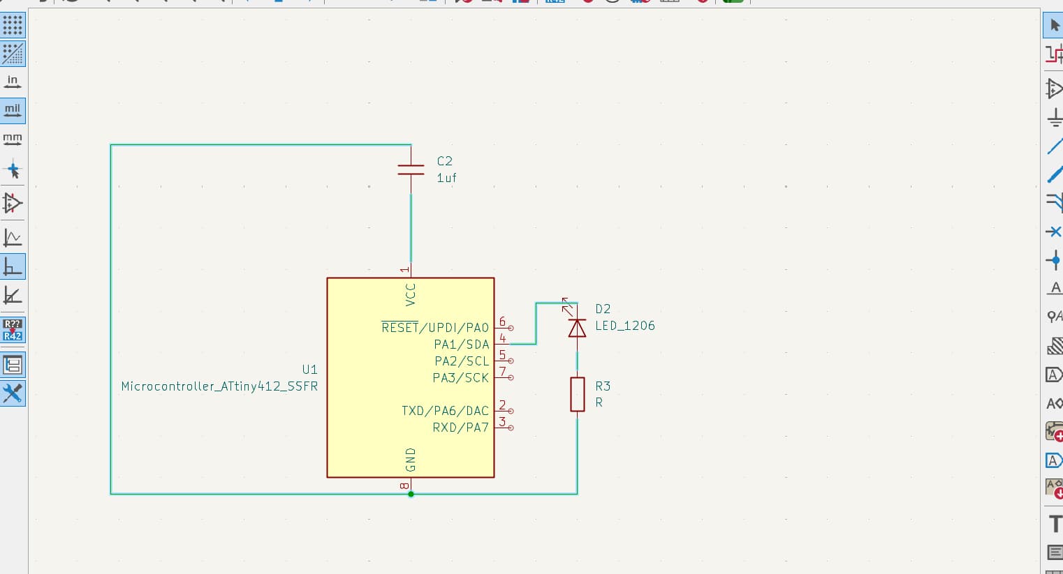
2. Global Labels:
Instead of drawing long wires, labels with the same name are used to connect points logically.
The same label should be used on the microcontroller pin and the component pin to create the connections.
Place a global lablel is like giving a global variable, which can me used through out.
For that either press "ctrl + L" or from the right tool select "place gloabl label."
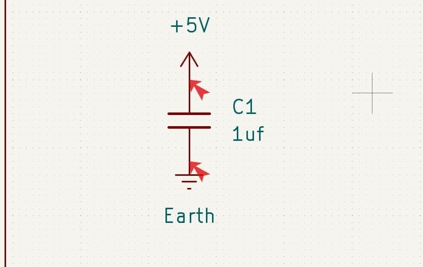
Ground(GND)
Qty.5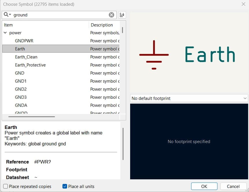
GND is the 0V reference point of the circuit where the current returns after flowing through the circuit.
GND can appear in different forms such as GND, Earth, or other symbols; here I selected Earth symbol.
VCC
Qty.4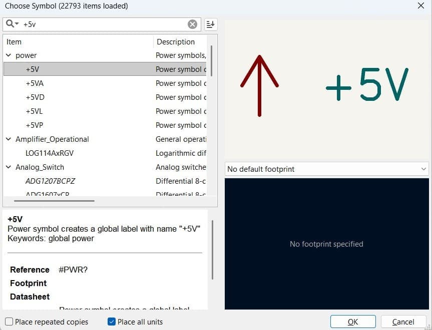
Voltage at the Common Collector.
For VCC, which represents the positive supply voltage, search for the "+5V"power symbol and place it in the schematic.
LED Series Resistor Calculator
As I was using an LED on my PCB, I needed to find out what the appropriate resistor value to limit the current and protect the LED. For that, I used this calculator by DigiKey .
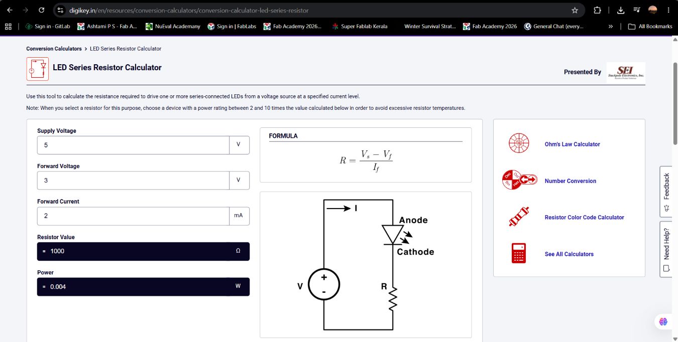
Supply Voltage (Vs)
The voltage supplied by the circuit or power source. For most microcontroller circuits, this is typically 5 V.
Forward Voltage (Vf)
The voltage drop across the LED when it is turned ON. A standard red LED typically has a forward voltage of 1.8–2.1 V (commonly taken as 2.0 V if the datasheet is unavailable).
Forward Current (If)
The recommended operating current of the LED. Most standard 3 mm and 5 mm red LEDs are designed to operate at 20 mA (0.02 A).
Values added in calculator
Supply Voltage = 5 V
Forward Voltage = 2 V
Forward Current = 20 mA
Calculated resistor value: 1k ohm
Power: 0.004W
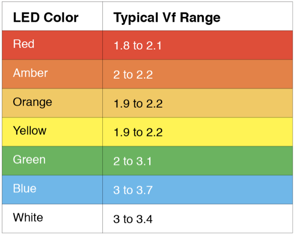
Chatgpt_AI Prompt Used
suppose if i'm using red led then what forward voltage vf, forward current If and supply voltage. Explain
source: Digikey
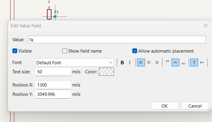
Adding values to components
To rename or give a value to a resistor or capacitor, double-click on the name like R or C_1206 and change it to the value you want. For example, I wanted 1k resistor and 1 µf capacitor. This is just for labeling in the schematic, so we know which value component to use. It does not actually set the value, it only shows the value in the design.
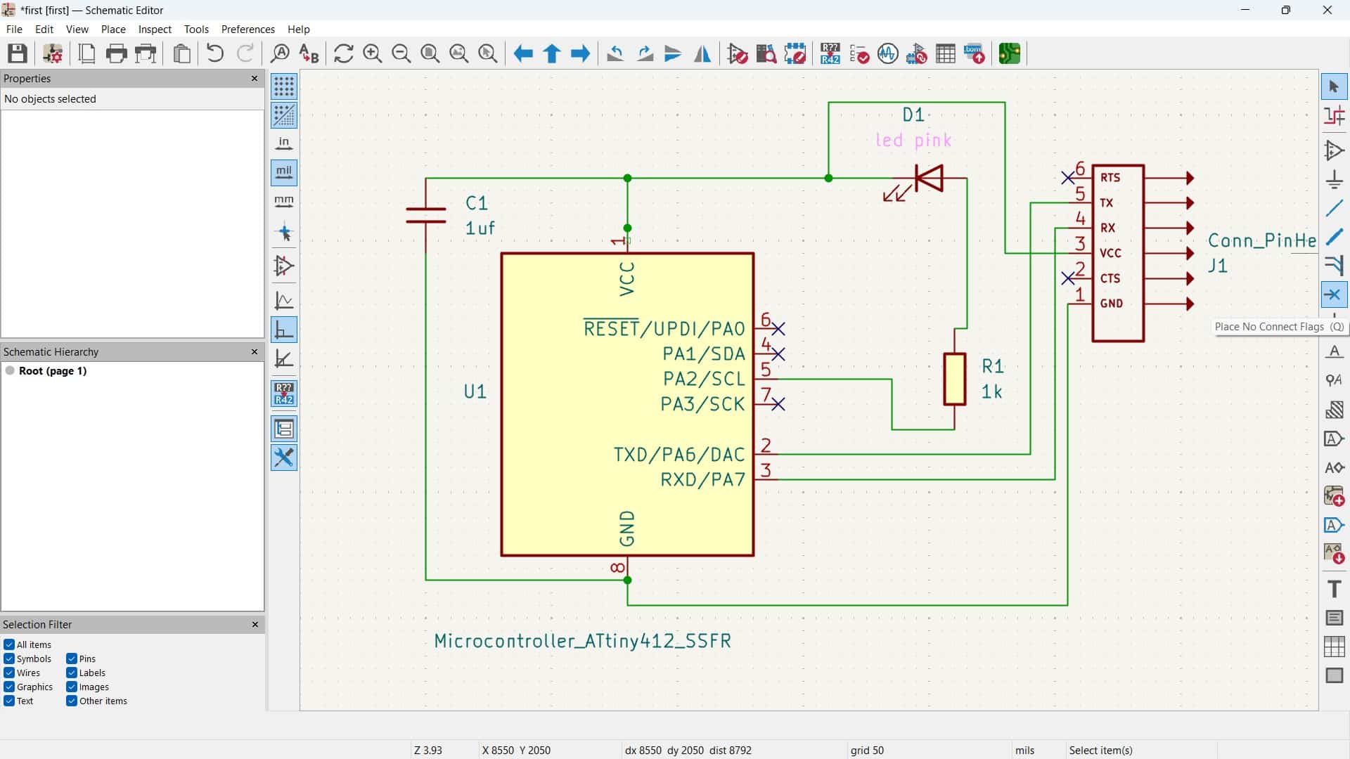
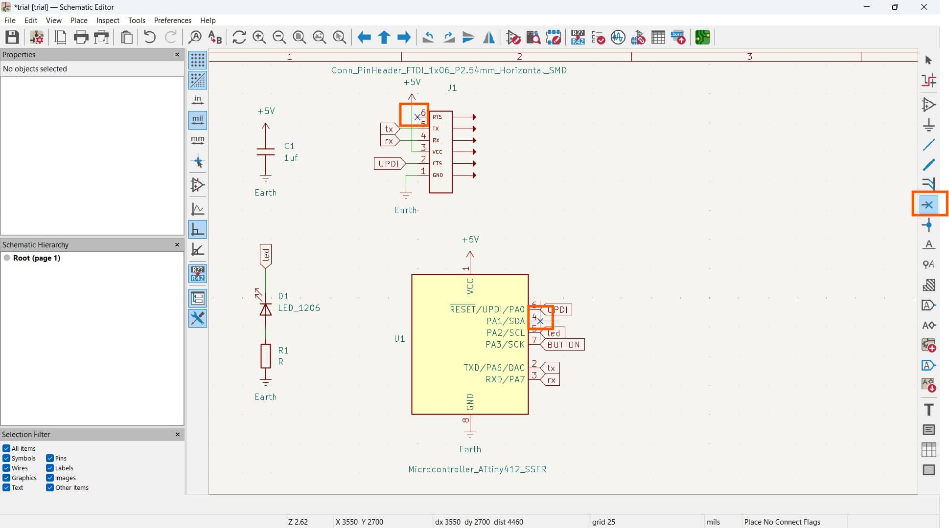
Crossing unconnected pins
After connecting the symbols, some ports were left unconnected. So i used Place No Connect Flag (Q) , which comes with a cross symbol and placed it on those pins. It indicates that the pin is intentionally left unconnected, which helps avoid ERC (Electrical Rules Check) warnings and errors in the schematic.
Organizing the Schematic for better documentation
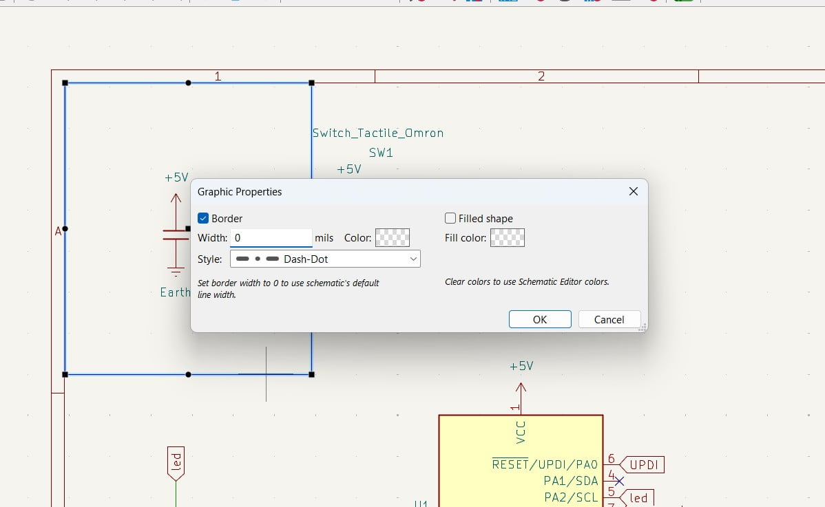
To organize the schematic, I used the Rectangle tool to group components. At first, I tried dragging directly, thinking it would draw the rectangle, but that only worked for selection, not for creating the rectangle. So the correct way was to click once from where it needed to start and then dragged it, making the component circuit inside the rectangle. After placing the rectangle, I clicked on it to change its properties, such as the line type, color, width, border style, or making it filled.
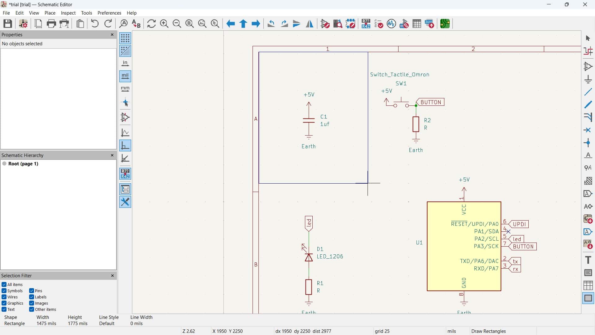
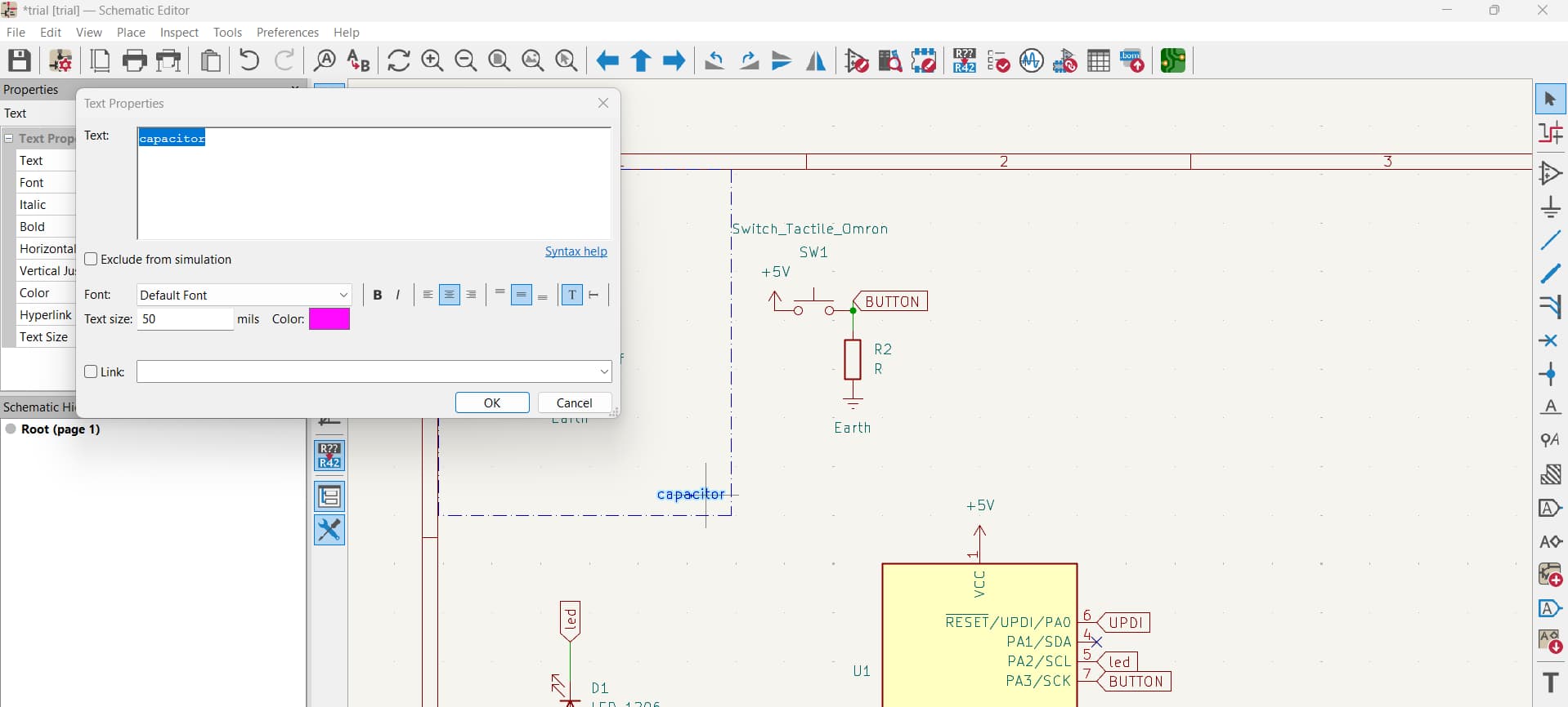
For adding text, I used the Text tool (T). After placing the text, I could change the font type, color, and size from the text properties. This helped label and organize the schematic clearly.
Connection Check
Using ~ (tilde, the key above Tab): to check the components connected to the microcontroller.
Place the pointer over a component's symbol and press ~, the component turns pink, and the connection of that to the microcontroller also turns pink.
This shows where the connection goes and which components are connected to it, helping verify that the microcontroller connections are correct.
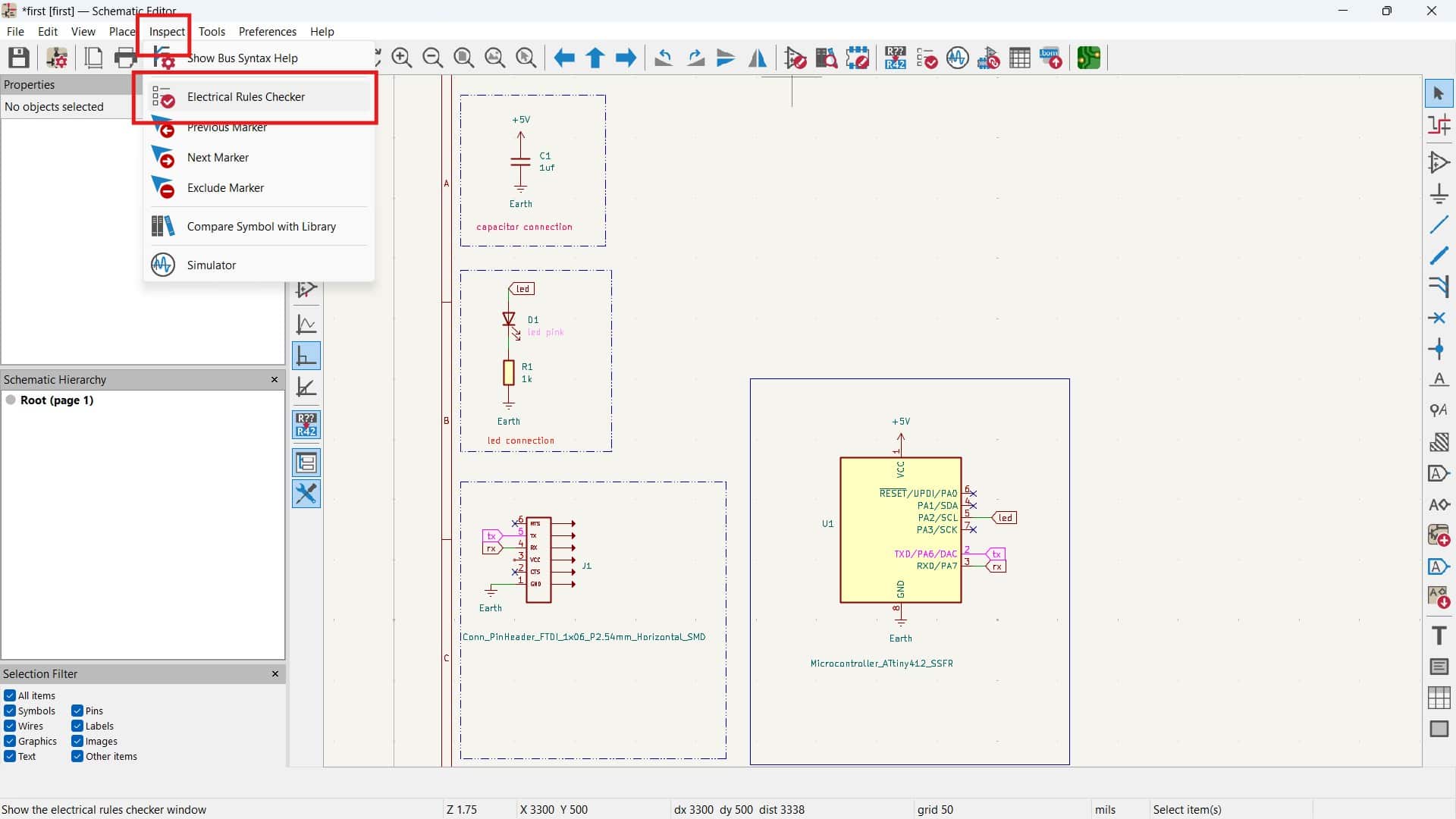
Run ERC (Electrical Rules Check)
Then run ERC (Electrical Rules Check) to find errors or warnings like missing connections or unconnected pins before moving to the PCB editor. Some warnings can be ignored if you have proper reason for that, as mentioned by the instructor, but errors should not be ignored.
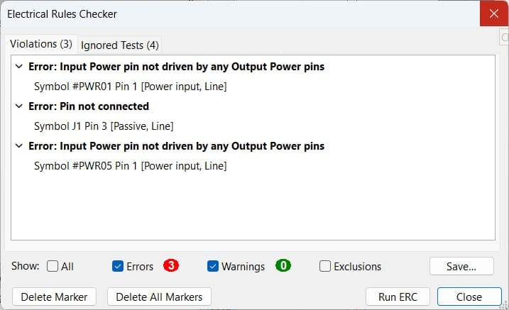
When running ERC, the error "Input power pin not driven by any Output Power pins" appears for the power and ground connections because KiCad cannot detect the power source.
Powerflag
Qty.2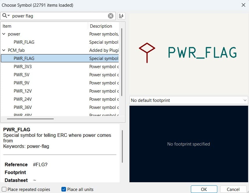
PWR_FLAG
This can be fixed by adding a PWR_FLAG to the power line, which tells KiCad that the net is being powered. After adding the PWR_FLAG, the error for the power connection disappears.
Final Schematic Design
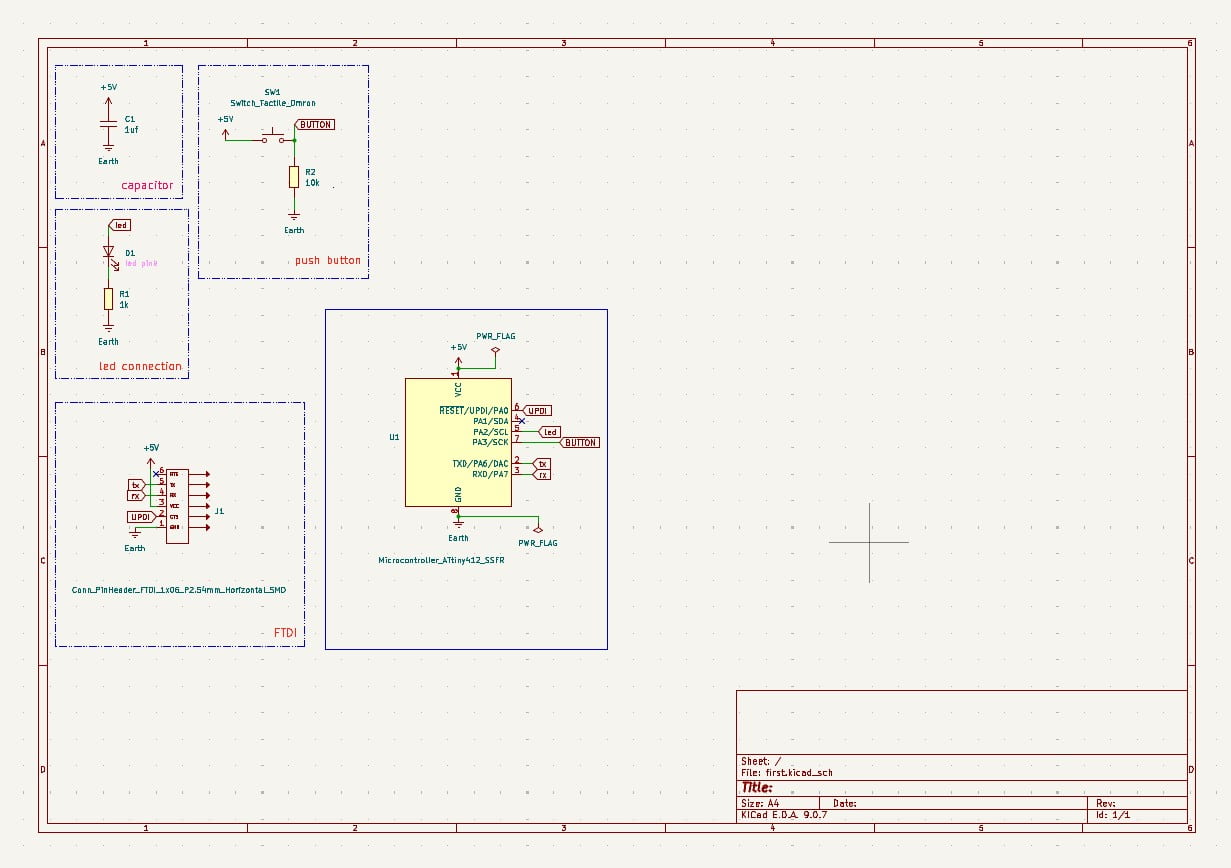
Download: schematicdesign
Converting the Circuit to PCB Layout
Using ![]() switch to PCB Editor and open the PCB in the PCB Editor window from the schematic window.
switch to PCB Editor and open the PCB in the PCB Editor window from the schematic window.
Using ![]() Update PCB from Schematic Editor, the symbols from the schematic are brought
into the PCB editor as footprints.
This tool is also useful later if any changes or updates are made in the schematic editor,
as it allows the PCB to be updated again while iterating on the design.
Update PCB from Schematic Editor, the symbols from the schematic are brought
into the PCB editor as footprints.
This tool is also useful later if any changes or updates are made in the schematic editor,
as it allows the PCB to be updated again while iterating on the design.
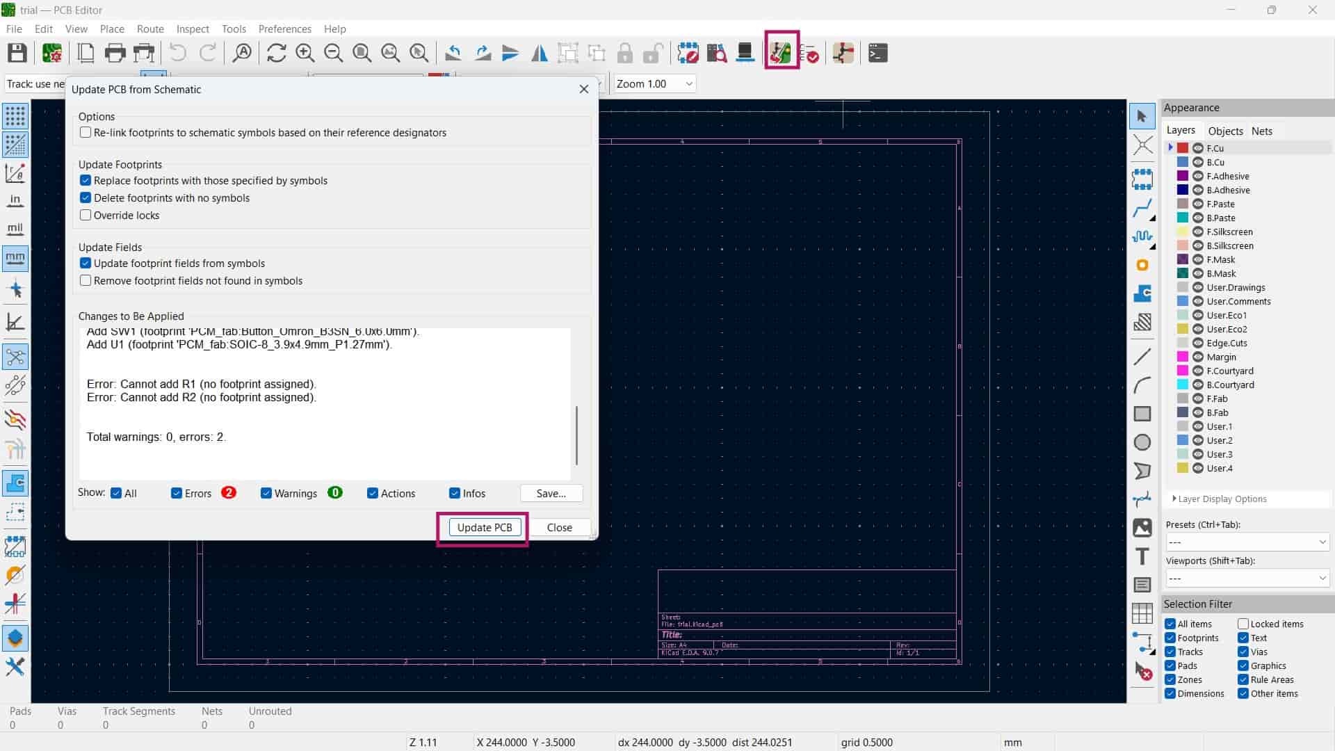
As it got updated, closed the pcb update tab; I was like where is my pcb footprints.
It turned out to be in the top left corner, far from work area. Just move them to work area, for moving a component press "M".
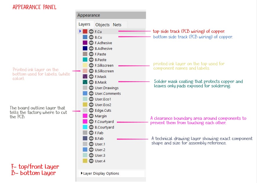
The white footprint labels were covering the components and making the layout hard to see.
Since these labels are in the F.Fab layer, the F.Fab layer was turned off from the Appearance panel. This hid the labels, which made it much easier for me to view and arrange the components in the PCB editor.
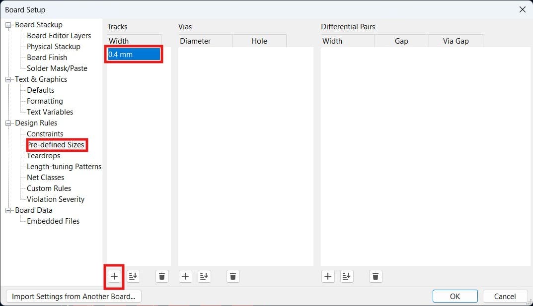
Board Setup: Design Rule setup >> Constraints
Before routing the tracks, the constraints were updated according to the milling capabilities of our lab machine.
So I went to Board Setup >> Design Rules >> Constraints and updated the values.
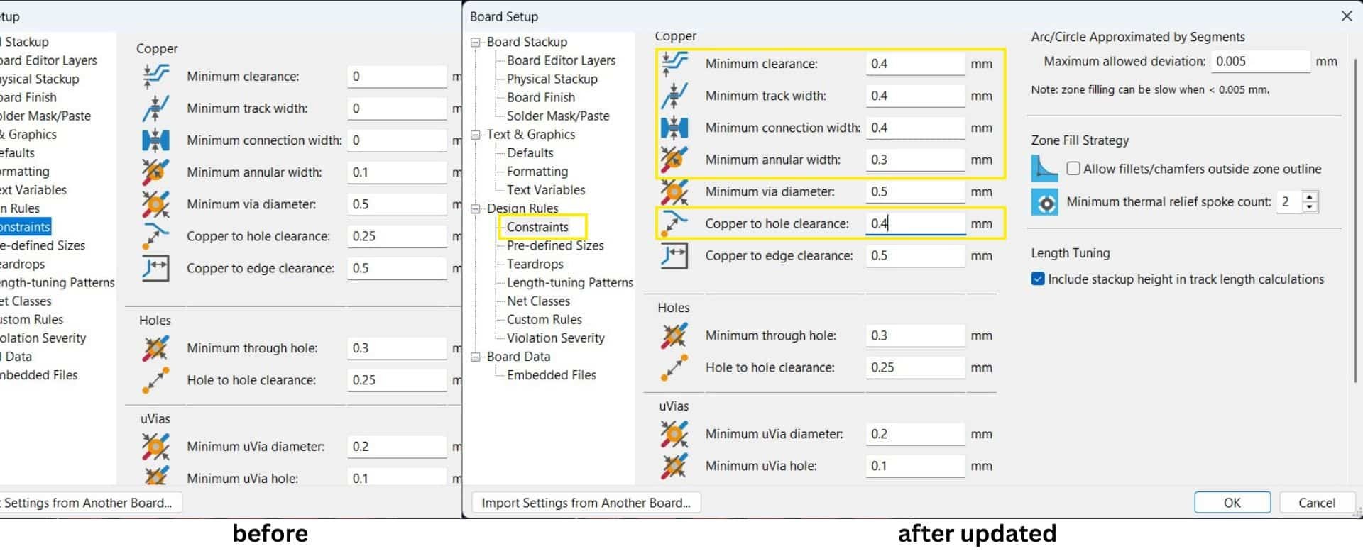
Then in Predefined Sizes, the track width was set to 0.4 mm and saved.
This was done because the milling tool in the lab has a minimum width it can safely cut.
If the tracks or clearances are too small, the machine may not mill them properly or the traces may get damaged.
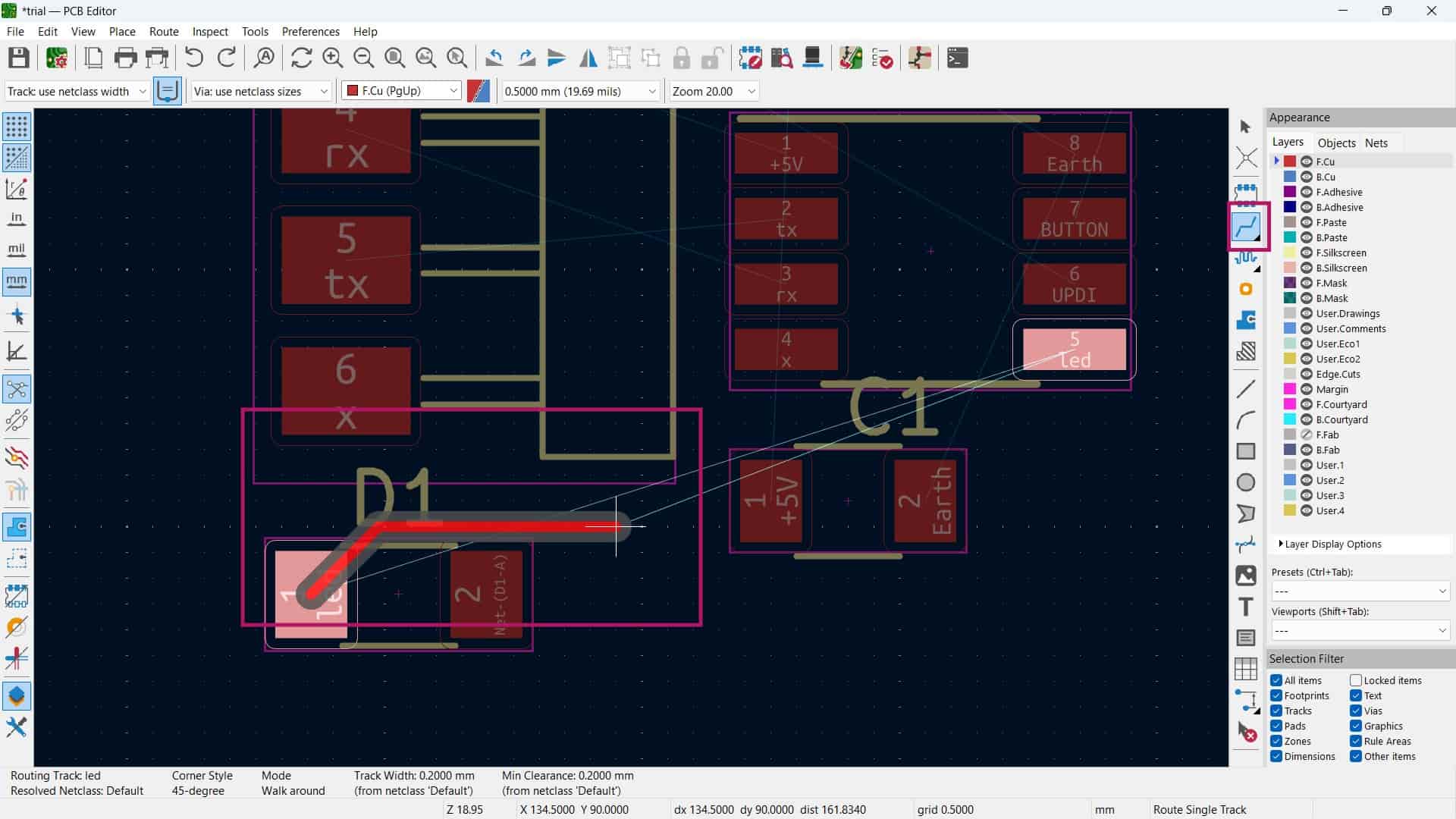
Route Tracks: Tracing
Route Tracks(X): Draws the copper connections between components on the PCB.
This step took me hours because each track had to find a path without crossing others.
It felt like solving a tricky puzzle. At first, it was fun.
Later, it became tiring when the connections didn't get solved easily.
After trying different arrangements and adjusting tracks, I finally managed to connect everything.
Finally, I felt a great sense of relief.
The routing was done on the F.Cu layer (Front Copper layer).
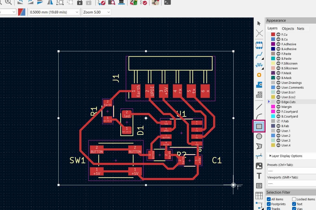
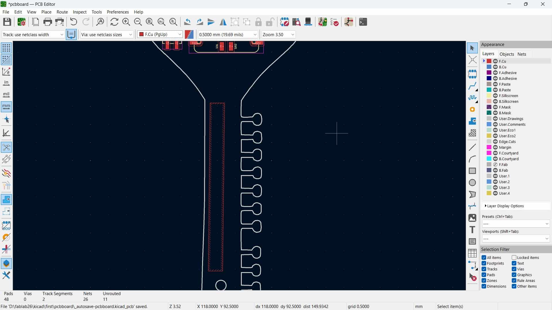
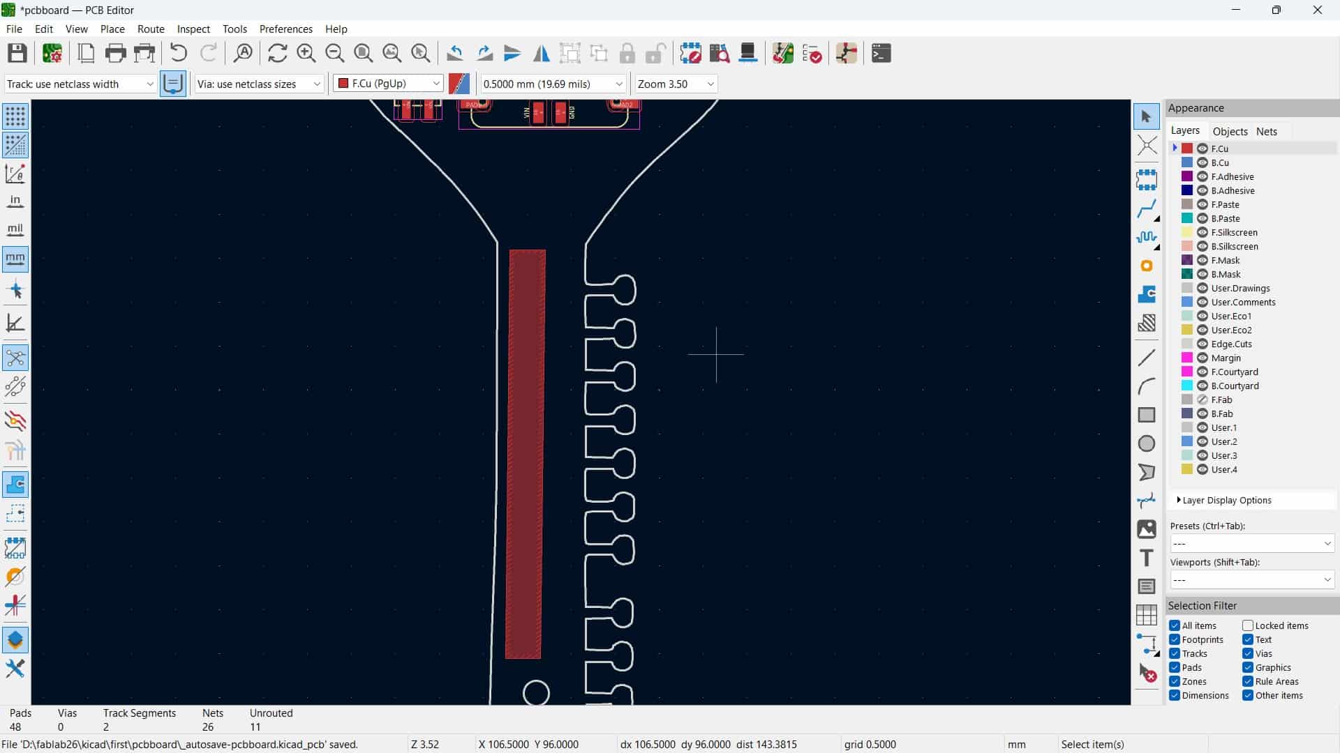
Board boundary: Edge cut drawing
After routing, a board boundary was created so the system knows the shape of the PCB and were the components is placed on,
which is also needed for the 3D view and milling.
For that, I used the Rectangle tool, making sure the rectangle was placed on the F.Edge.Cuts layer,
otherwise KiCad will not understand it as the board cut.
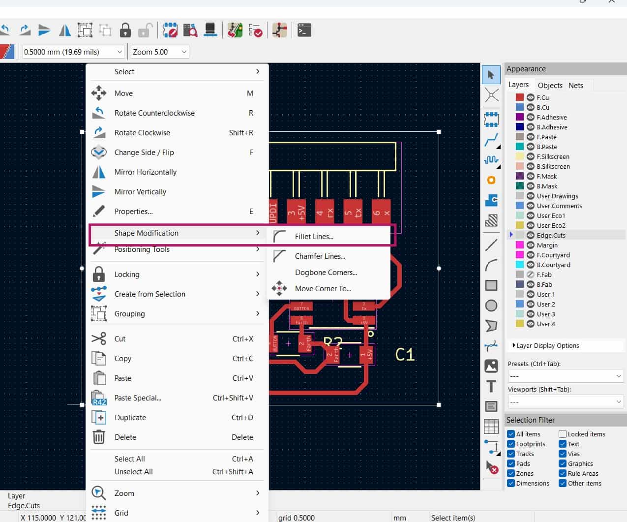
To give the board rounded corners, I right-clicked on the rectangle and selected Shape Modification >> Fillet Lines, then entered a value for the fillet.
I also wanted a hole in the board, so I used the Circle tool on the F.Edge.Cuts layer to create it.
My First Routing and Feedbacks
This is how I finally routed the tracks, and at that time I thought it was pretty fine. But during my regional and local review, a few areas to improve and learn were pointed out:
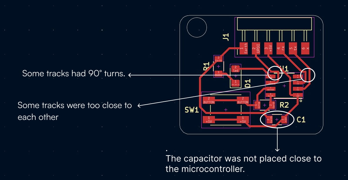
90° turns in tracks:
Sharp corners are not good practice and can make milling harder.
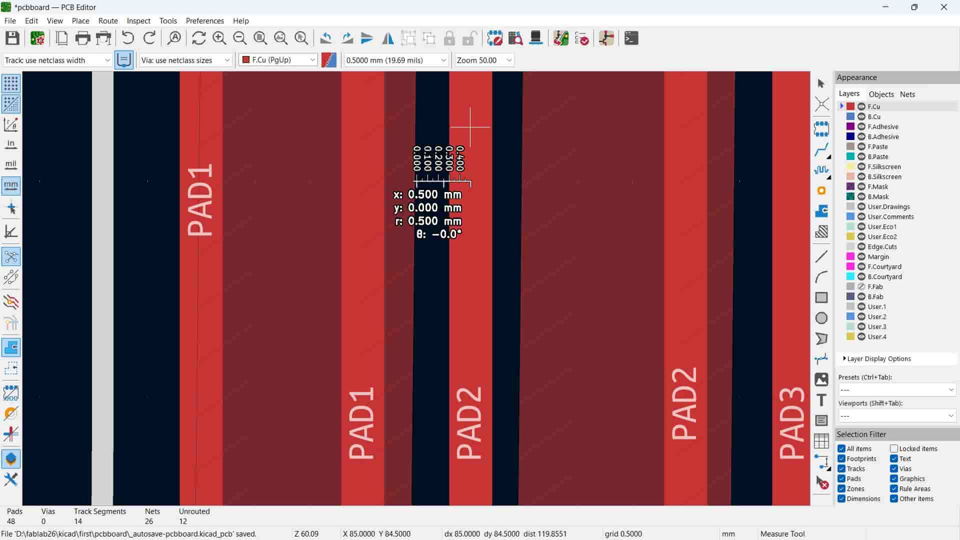
Tracks too close:
If tracks are very close, the milling tool may not separate them properly, which can cause short circuits.
Capacitor far from microcontroller:
As my instructor explained, if I placed water tank at your house far from mine, it would not be efficient when I need it.
It is better to keep the water near my house.
Similarly, the capacitor should be placed close to the microcontroller so it can quickly provide stable power when needed.
DRC: Design rules checker
Design Rule Check (DRC) verifies the PCB layout by automatically checking for design errors and manufacturing rule violations. It helps identify issues such as unconnected nets, insufficient clearances, overlapping objects before the PCB is fabricated.
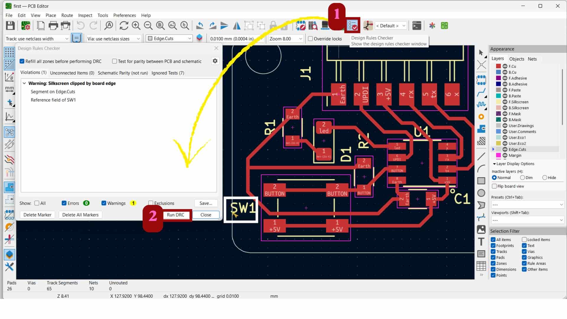
The warning was a silkscreen clipping warning for the SW1 reference. This warning was ignored as the PCB was fabricated without a silkscreen layer.
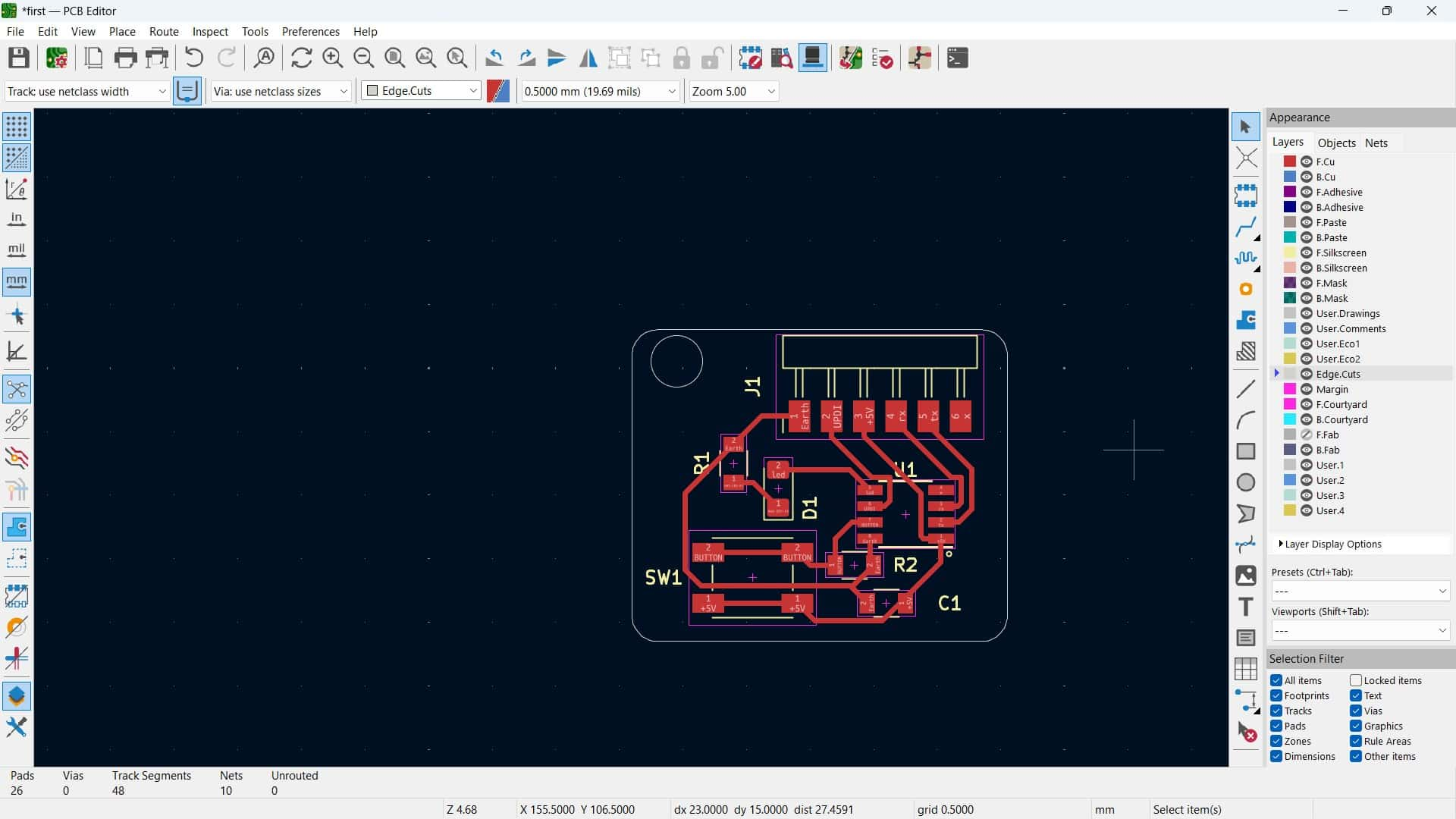
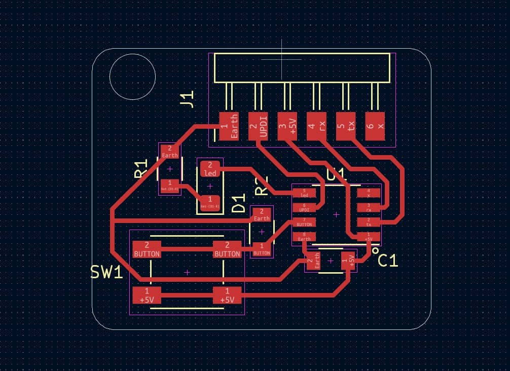
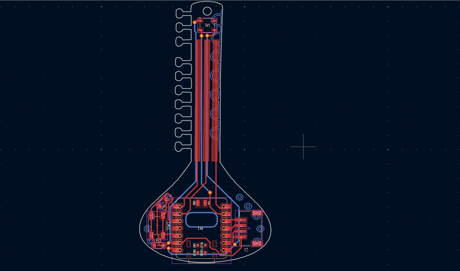
Final PCB Layout
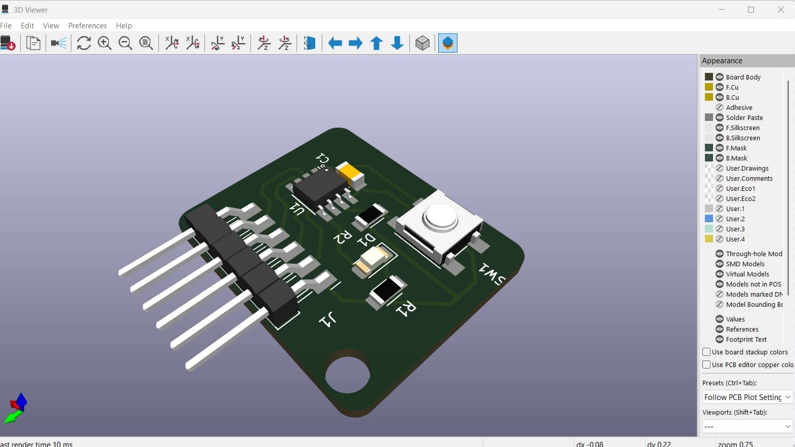
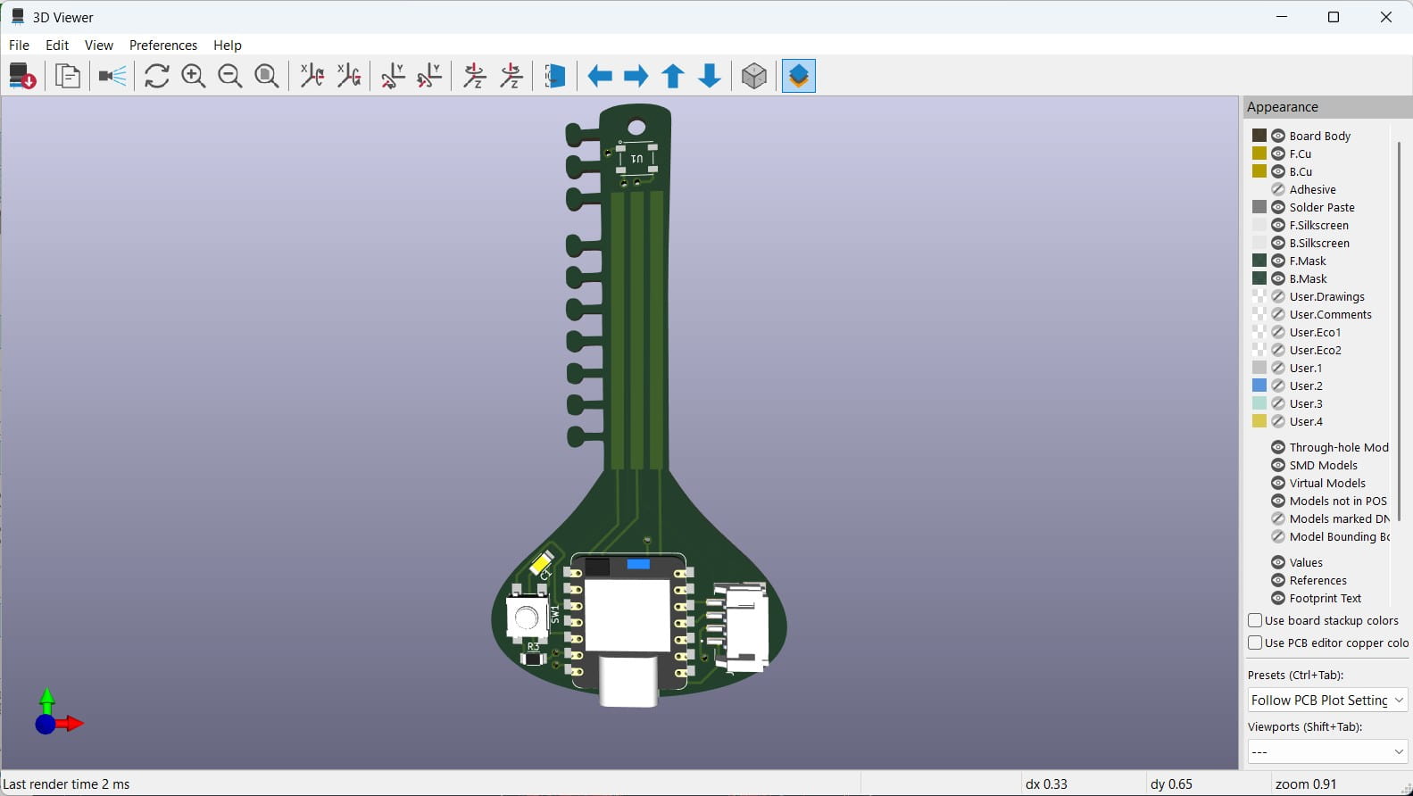
3D Viewer
Using ![]() the 3D Viewer, a new window opens where I can see the 3D visualization of the designed PCB.
the 3D Viewer, a new window opens where I can see the 3D visualization of the designed PCB.
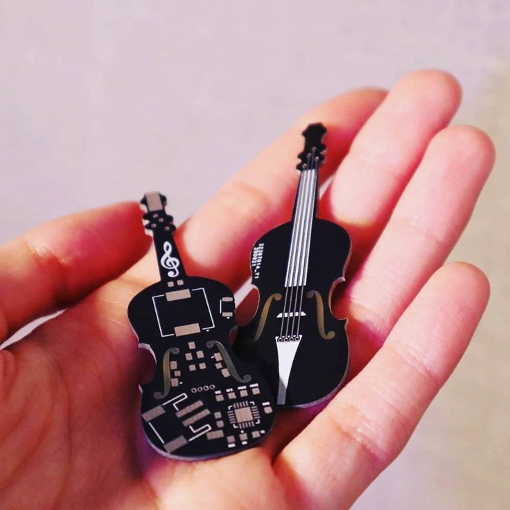
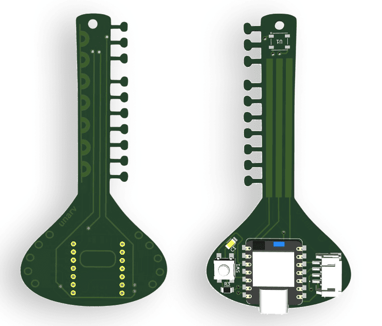
Desiging a custom PCB
For the custom PCB, the minimum requirements were a Seeed Studio XIAO, LED, resistor, capacitor, button, and an I²C pin.
At first, I had not decided the PCB shape. I thought about many forms like a shell, vase, flower, and others.
I also love instrumental music, and recently I have been listening to a lot of sitar music, which inspired me to make a sitar-shaped PCB.
I also saw a guitar-shaped PCB on Pinterest, which encouraged the idea.
Making the sitar shape was tricky because it is narrow,
making component placement difficult. With help from my instructor,
I managed to arrange the components and create the sitar-shaped board.
He also suggested adding touch pads, so when the board is connected to a computer, touching them could produce sound.
source: Guitar


The sitar is a traditional Indian string instrument used in Hindustani classical music (from Nouthern India).
It has a long neck and a rounded body, which gives it a deep and rich sound.
The sitar developed around the 16th-18th century, influenced by earlier Indian instruments like the veena.

source: veena
The veena is one of the oldest Indian instruments(Carnatic classical music from Southern India) and is believed to have originated in ancient India.
It is mentioned in ancient texts like the Vedas, which are more than 3000 years old.
Over time, musicians like Ravi Shankar helped bring the sitar to global audiences.
Today, artists like Anoushka Shankar and Rishab Rikhiram Sharma are also introducing sitar music to new listeners.
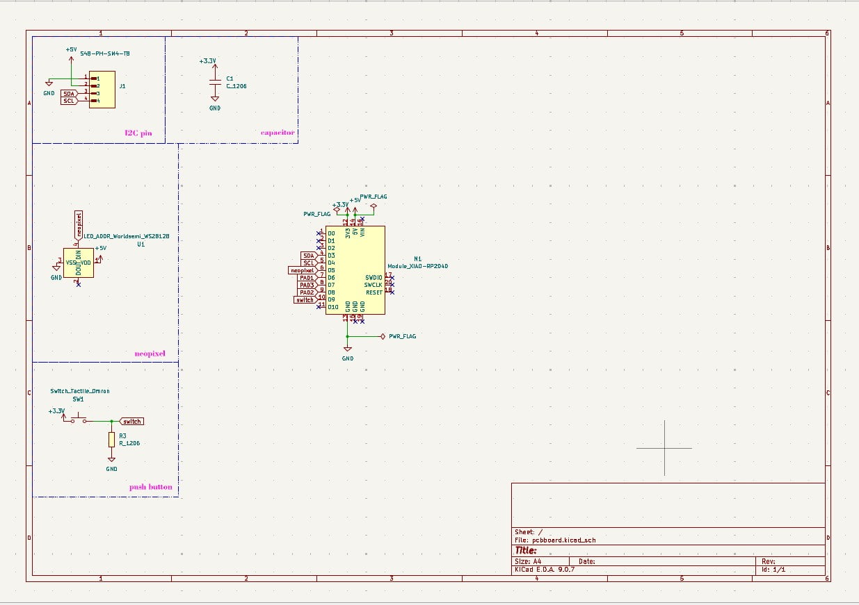
Desgning circuit in Schematic Editor
I started the circuit design using a XIAO RP2040, NeoPixel LED, resistor, capacitor, button, I2C pin, and a 1x6 pin header.
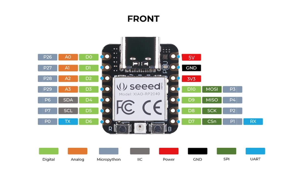
Seed Studio: XIAO-RP2040
Later, when placing the components inside the sitar shape, that the 1x6 header pin was quite large and not really necessary, so I removed it. This means the board does not have the header pin for external connections anymore.
For the I2C pins, I first used a 2x2 pin header, but later replaced it with another pin from the SnapMagic library, as suggested by my instructor.
It was like switching between the schematic editor and PCB editor, changing the pin connections in the schematic, changing headers here and there, and then switching back to the PCB editor again, going back and forth while iterating the design
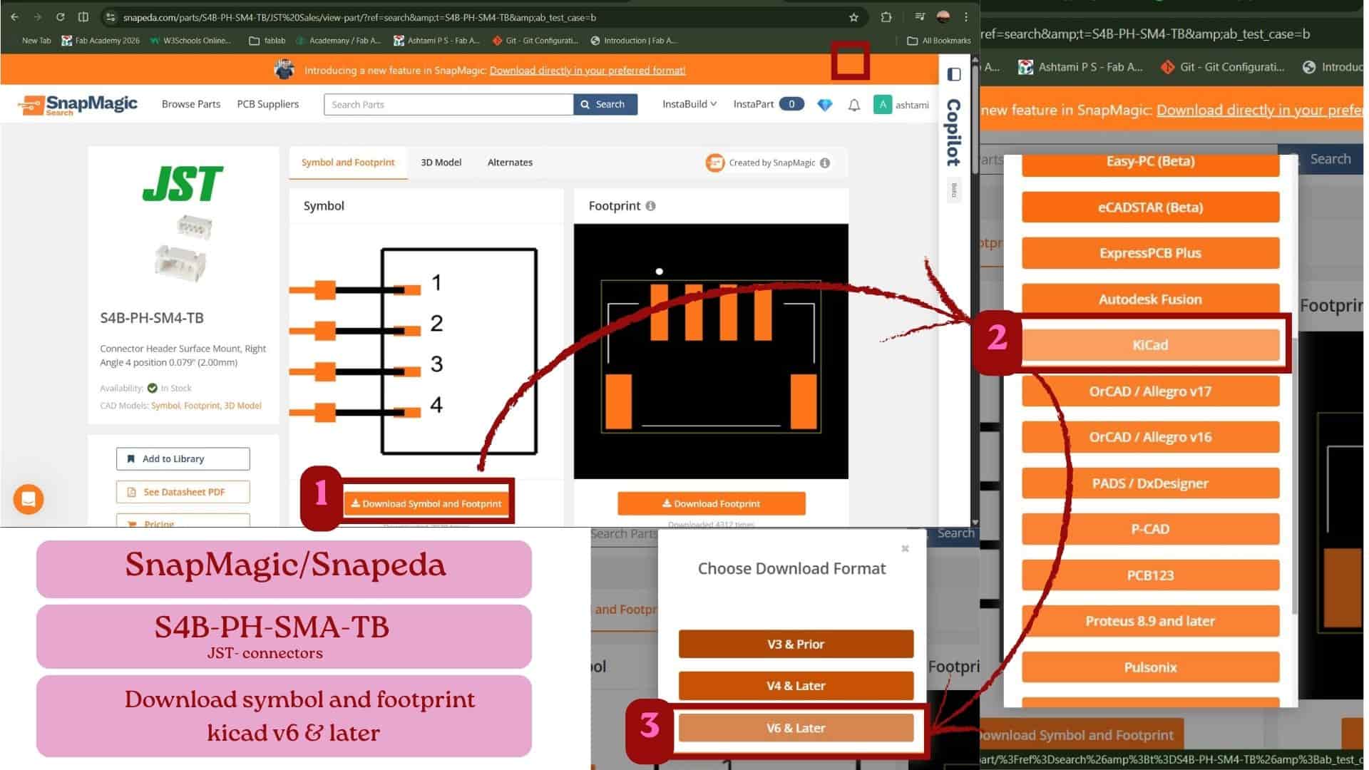
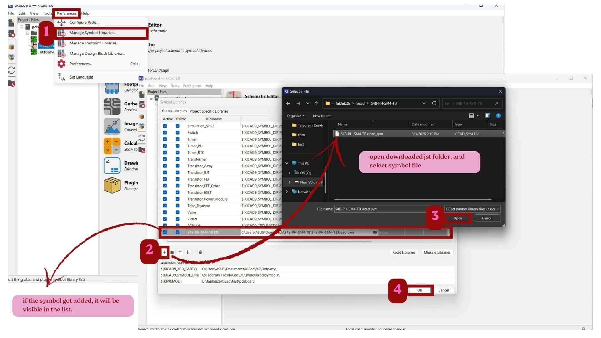
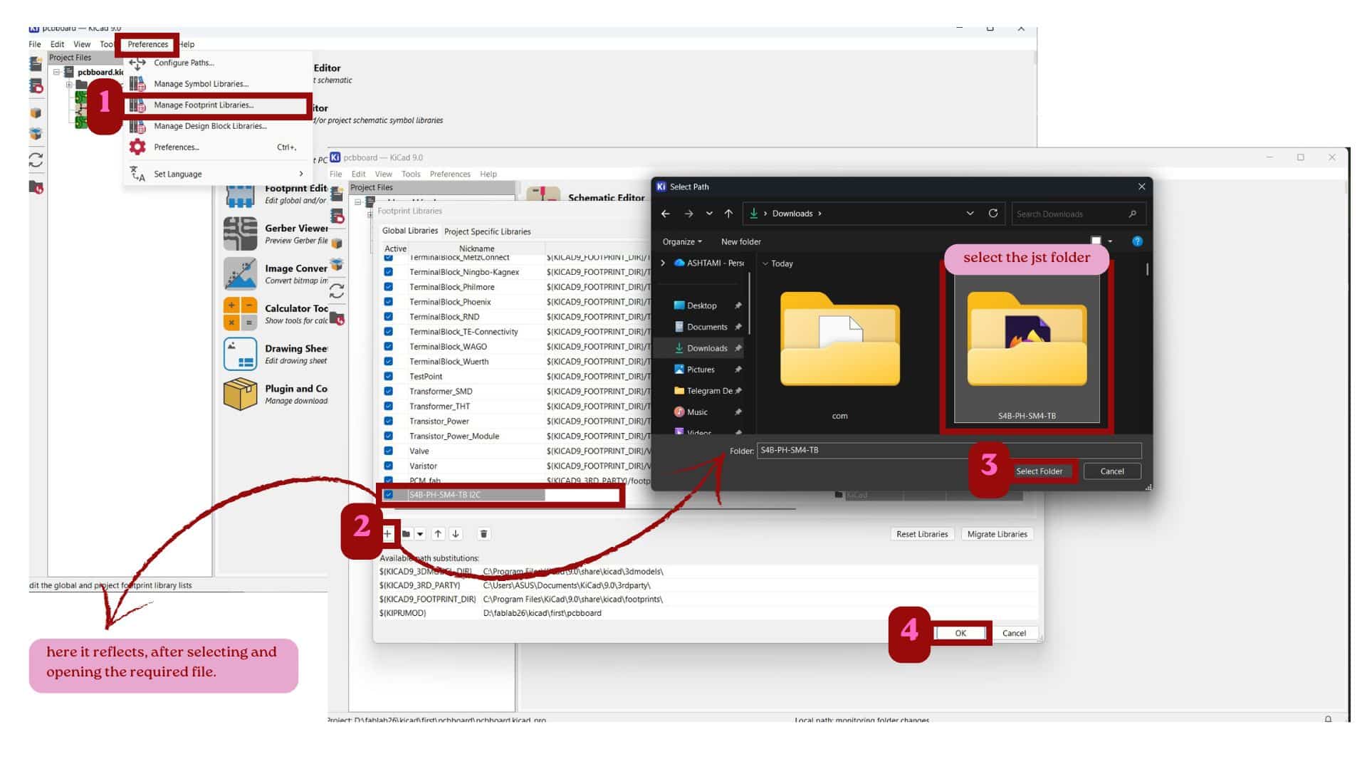
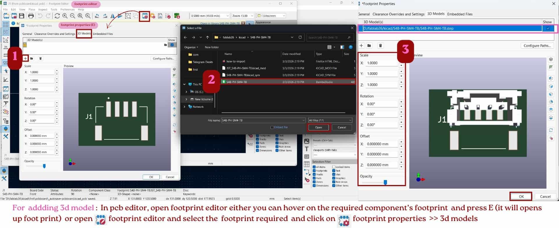
SnapMagic/SnapEDA: downloading JST connector
SnapMagic/SnapEDA: Online electronic component libraries where we can download component symbols, PCB footprints, and 3D models and import to kicad.
Components and their symbols used:
Development board
Qty.1
Xiao rp2040
Neopixel
Qty.1LED_ADDR_Worldsemi_WS2812B
Resistor
Qty.2
R_1206
Capacitor
Qty.1
C_1206
Push BUtton
Qty.1
Switch_Tactile_Omron
Pin header I2C
Qty.1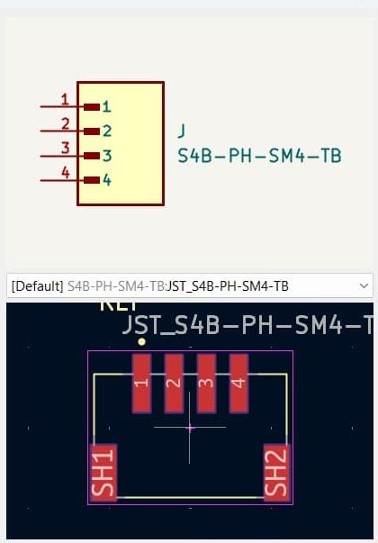
S4B-PH-SM4-TB
Ground(GND)
Qty.5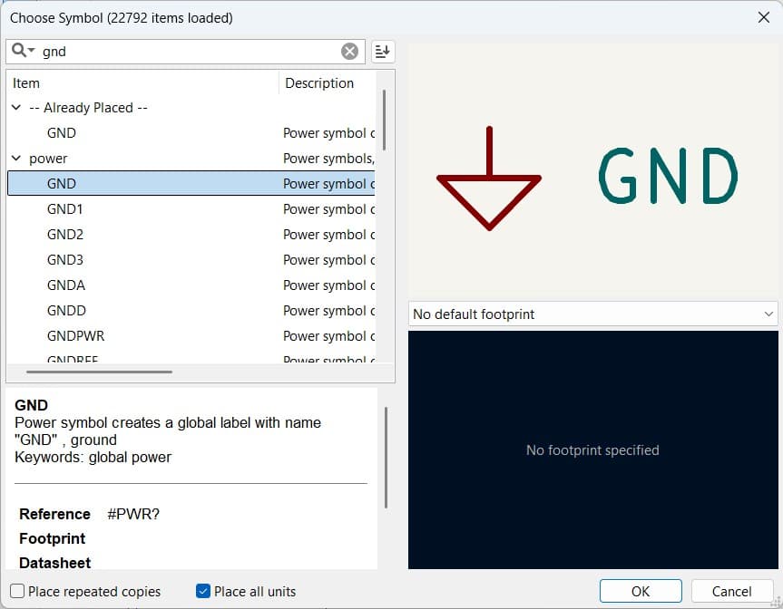
GND
VCC
Qty.4
+5v
VCC
Qty.3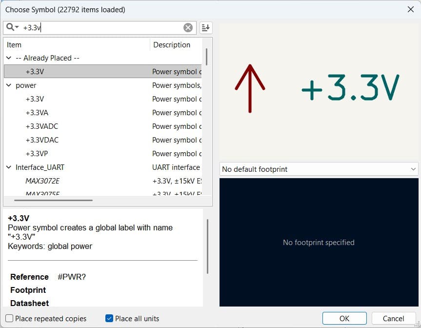
+3.3v
Powerflag
Qty.2
PWR_FLAG
Schematic Design
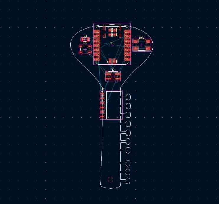
Designing the PCB in the PCB Editor
Don't even ask me how much time it took to figure out routing the tracks.
At first, I was trying to route everything only on the top layer, which made it very difficult.
Later, I placed the I2C pin on the bottom side to make routing easier.
The front layer (F.Cu) is the top copper layer of the PCB, where components and tracks can be placed.
The bottom layer (B.Cu) is the bottom copper layer, where tracks can also be routed.
Using both layers gives more space to route connections when the circuit becomes complex.
There was also another constraint while making this PCB: the board size. Our instructor initially said the board should be 48 mm x 70 mm. I tried resizing the sitar shape in inkscape to fit within that size. I also made a rectangle for the XIAO size (around 20 mm x 17.5 mm) to understand how much space it would take. Because the sitar shape is narrow, it was difficult to fit the components inside. Later, the instructor allowed the board to be slightly bigger, and the final board size became around 91 mm x 46 mm.
Drawing touch pads
To create the capacitive touch pads, I used the![]() Draw Filled Zone tool (Ctrl + Shift + Z).
I selected the F.Cu (Front Copper) layer because I wanted the touch pads on the top copper layer of the PCB.
Draw Filled Zone tool (Ctrl + Shift + Z).
I selected the F.Cu (Front Copper) layer because I wanted the touch pads on the top copper layer of the PCB.
After drawing a rectangular pad, I pressed B to refill the copper zone.
Finally, I duplicated the pad using copy and paste to create a total of three touch pads.
2-side layer trace
Since my PCB is a 2-layer board, I routed traces on both the Front Copper (F.Cu) and Back Copper (B.Cu) layers.
- For routing, on the bottom layer press B.
- To adjust an existing trace without breaking its connections, use D (Drag)
- Use M (Move) to move objects freely
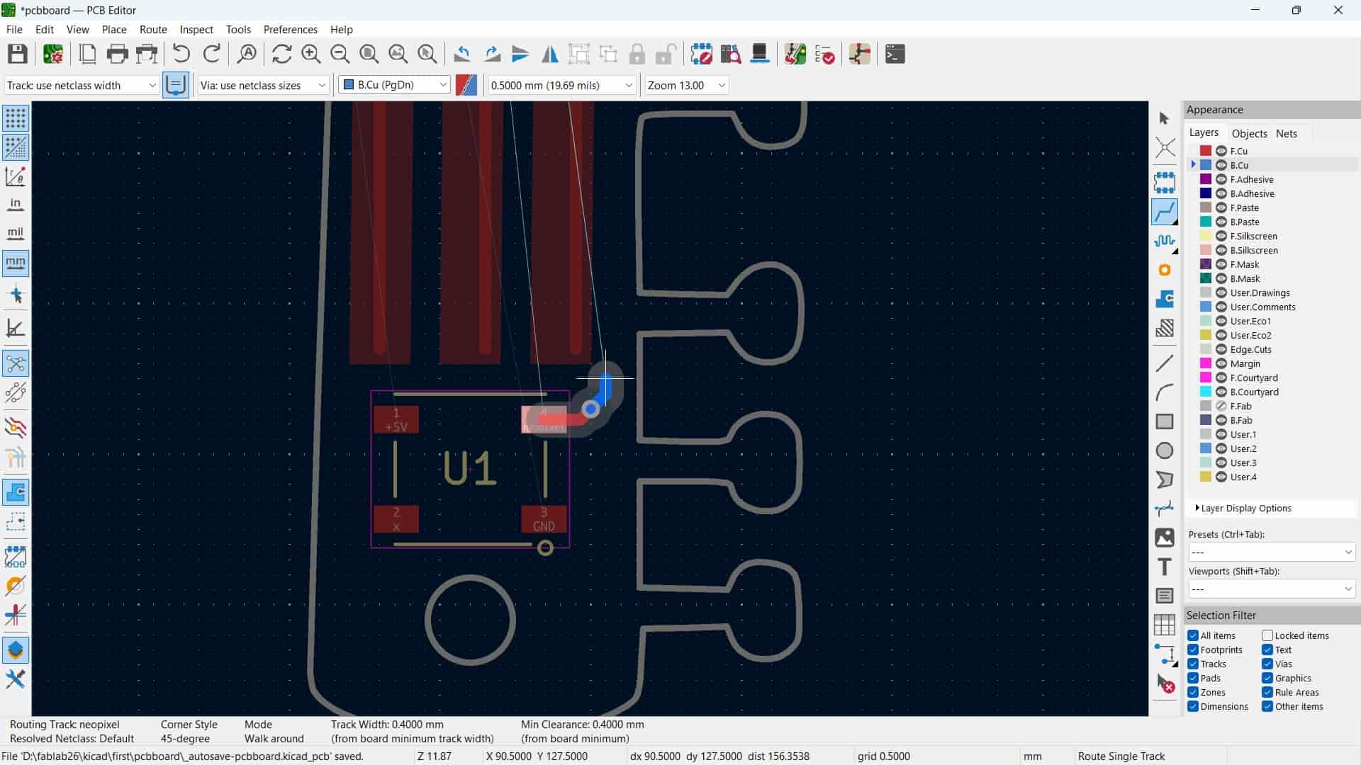
As all the components, including the Seeed Studio XIAO, were mounted and soldered on the front layer, the traces routed on the bottom layer had to be brought back to the front layer before connecting to the component pads. This was done by placing a via, which creates an drill hole , using copper wires/rivet create connection between the two copper layers during production. A via can be inserted by selecting Place Via, or while routing a track,pressing V to place a via and continue routing on the opposite layer.
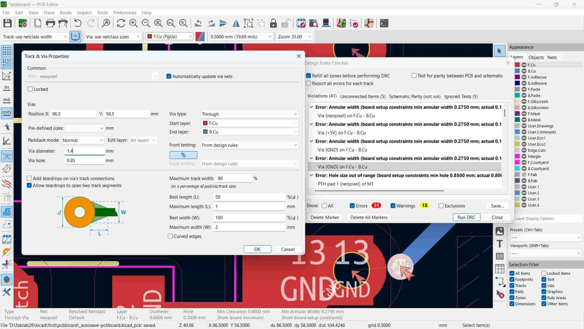
DRC: Design Rules Check
While running the DRC, I found errors related to the via size and hole diameter. The default via dimensions were smaller than the board design rules, so I increased the via diameter to 1.4 mm and the hole size to 0.85 mm, which resolved the errors.
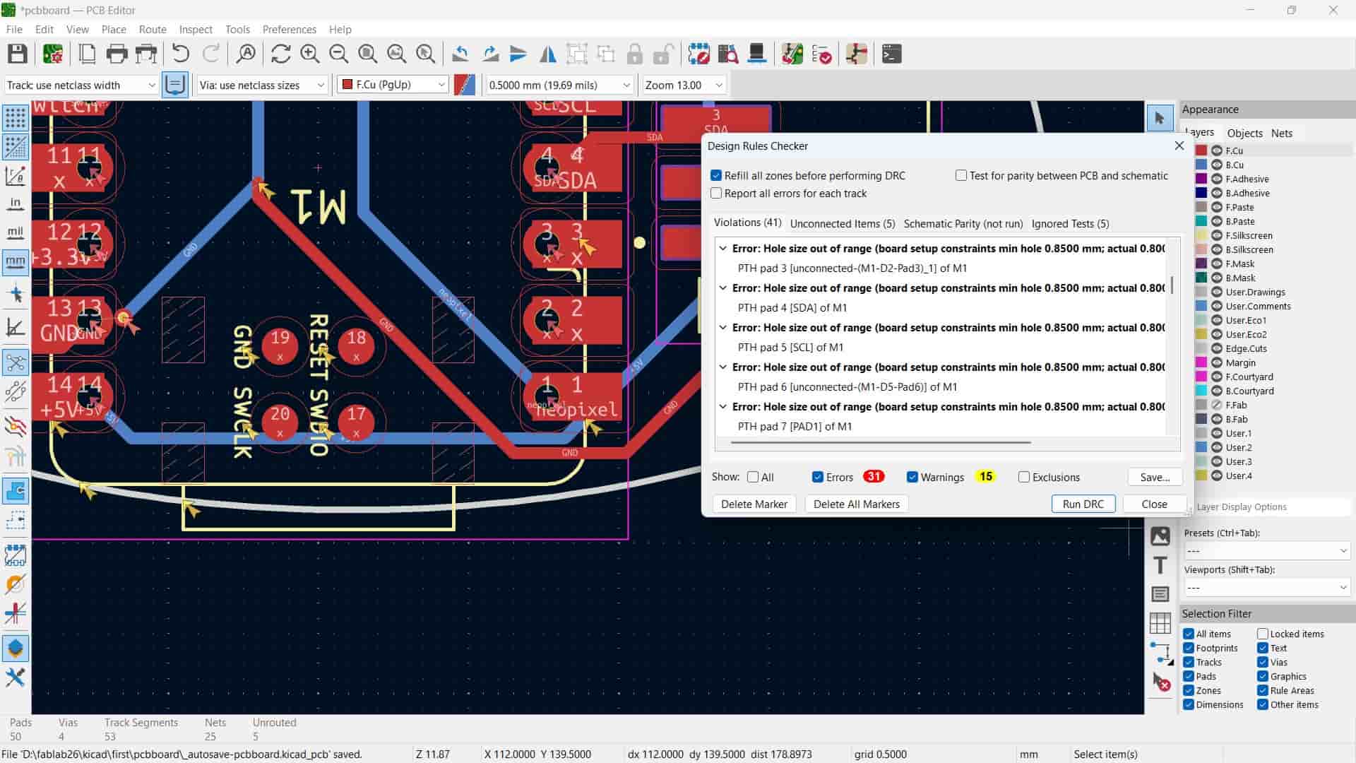
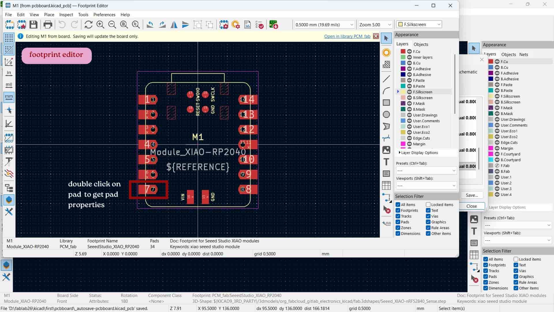
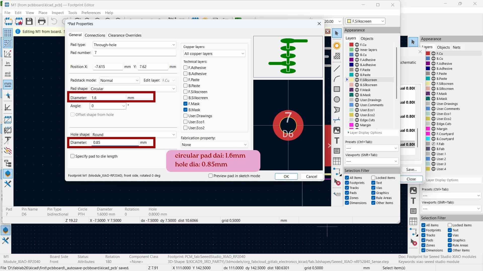
There was also errors with the Seeed Studio XIAO RP2040 footprint because its default pad hole diameter (0.8 mm) was smaller than the required 0.85 mm. I updated the pad hole diameter to 0.85 mm and circular pad diameter at 1.6 mm, and the DRC errors were cleared.
Board Boundary design in Inkscape
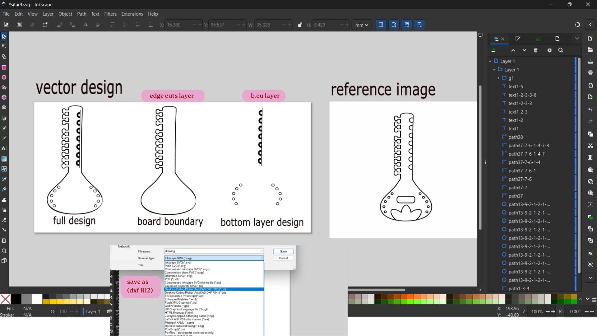
I used a reference image in Inkscape and converted it into a vector using the Trace Bitmap tool. After cleaning and editing the vector, I illustrated the bottom layer design using the Circle and Pen tools. Once the design was complete, I exported it as a DXF file for use in the CAD software. The bottom layer design shown here is my second iteration, as I redesigned it after an earlier version to improve the overall appearance and fit for production.
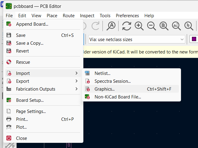
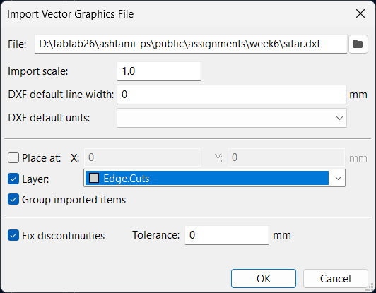
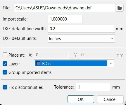
Import dxf to kicad
File >> Import >> Graphics >> Import Vector Graphics File: select the required dxf file and the layer.
3D viewer
this 3d model before changing the bottom vector design.
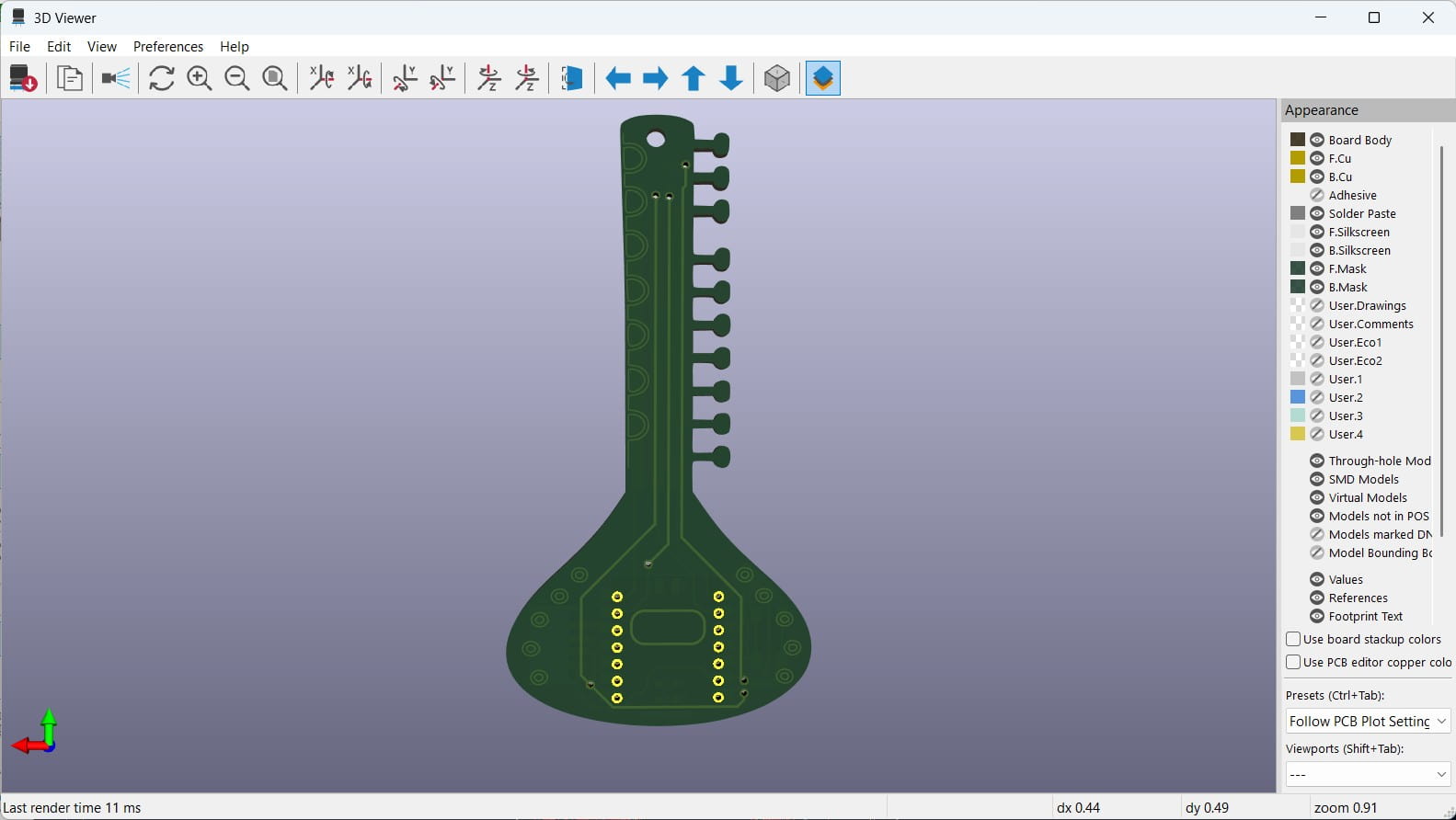
After changing the bottom vector design.
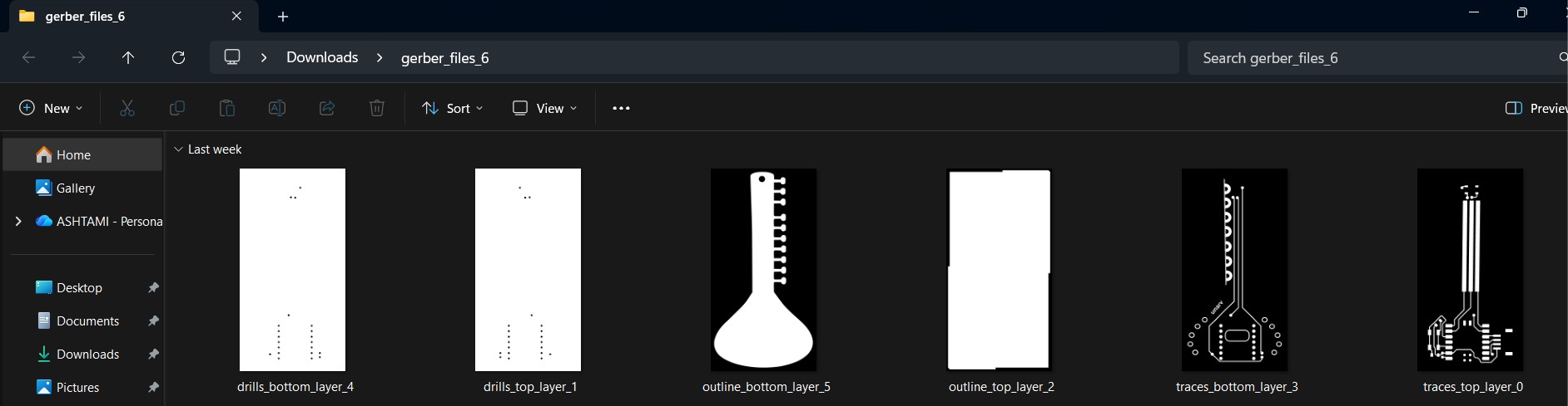
Gerber to PNG
In KiCad, Gerber files are used as the fabrication output files for PCB manufacturing.
The Gerber and drill files generated from KiCad are used to create the toolpaths for milling the PCB traces and cutting the board.
To get the Gerber files, go to Fabrication Outputs >> Gerbers >> Plot(exporting or generating the PCB manufacturing files from design).
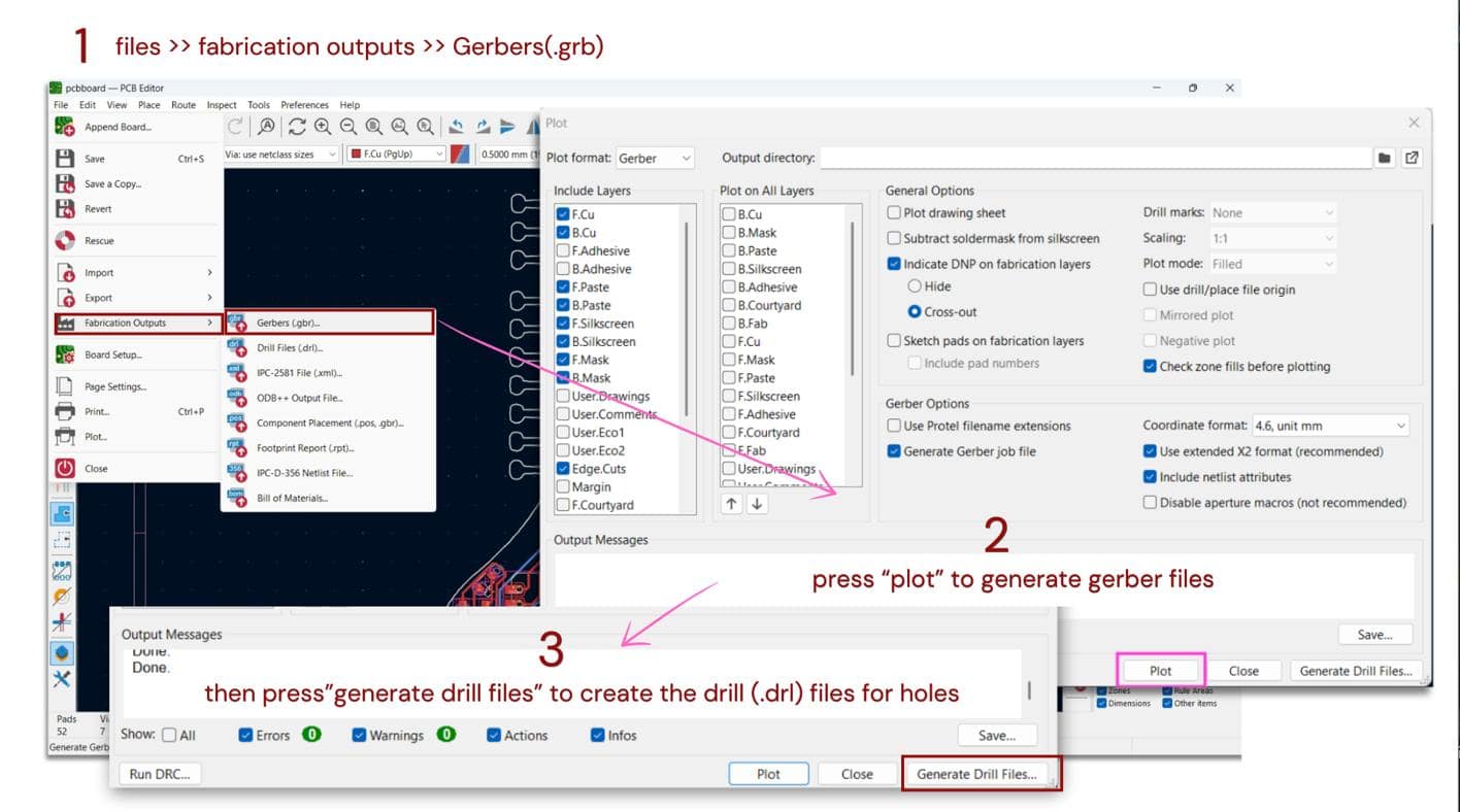
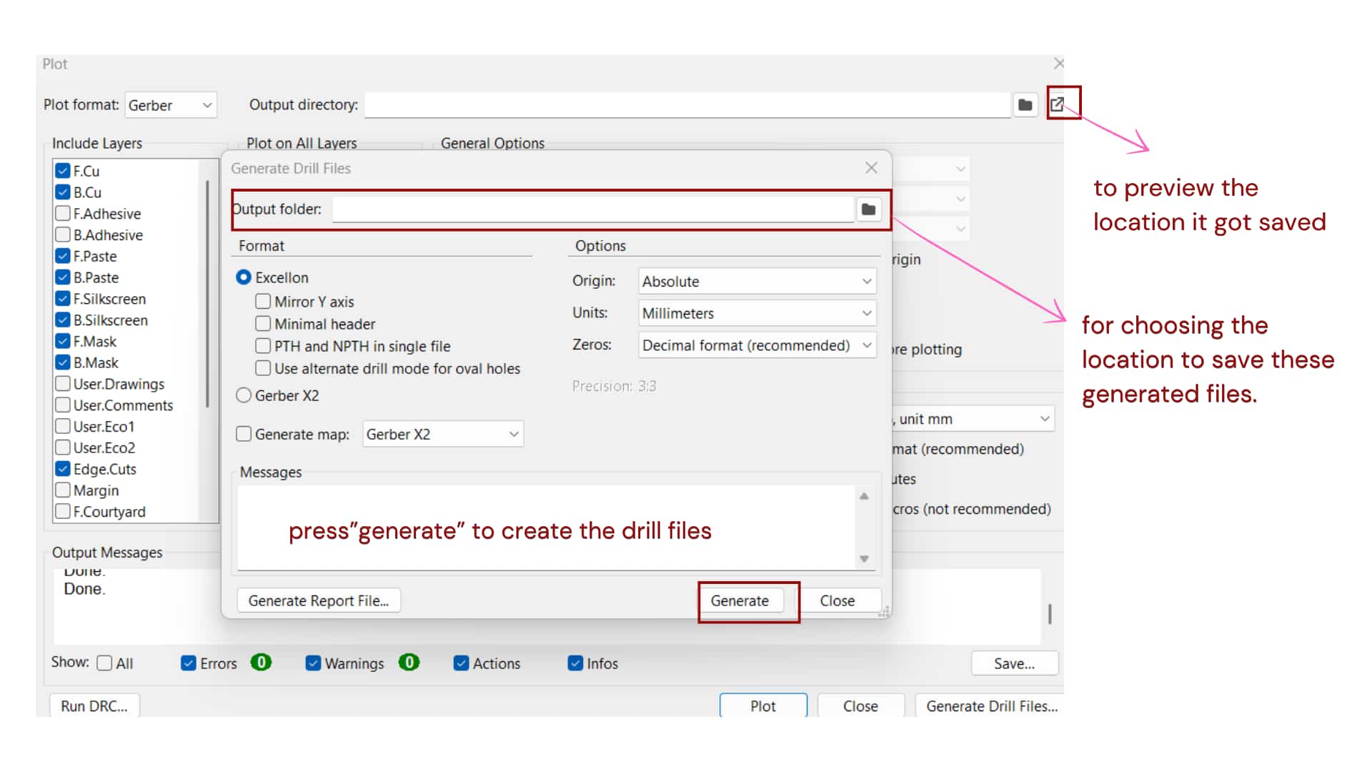
After plotting, Generate Drill Files to create the hole/drill data. Also it has option to choose the output folder if needed and then generate the files.
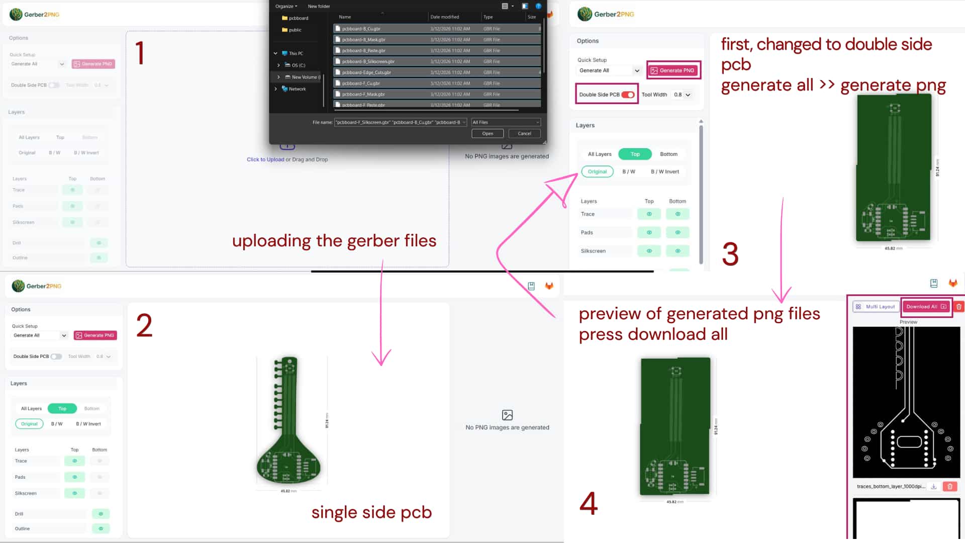
After generating the Gerber files in KiCad, the files were saved in a folder.
These files were then converted to PNG using Gerber2PNG.
(png file is used by the milling software to create the toolpath for cutting PCB traces and outline.)
All the generated files were uploaded to the website.
By default it creates a single-sided PCB, but since my design is double-sided,
I selected the double-sided option.
Then I clicked Generate All to create the PNG images.
The generated PNG files can be previewed on the right side,
and there is an option on the top to download all the images.
Later updates and improvement made:
This board was further improved in later assignments.
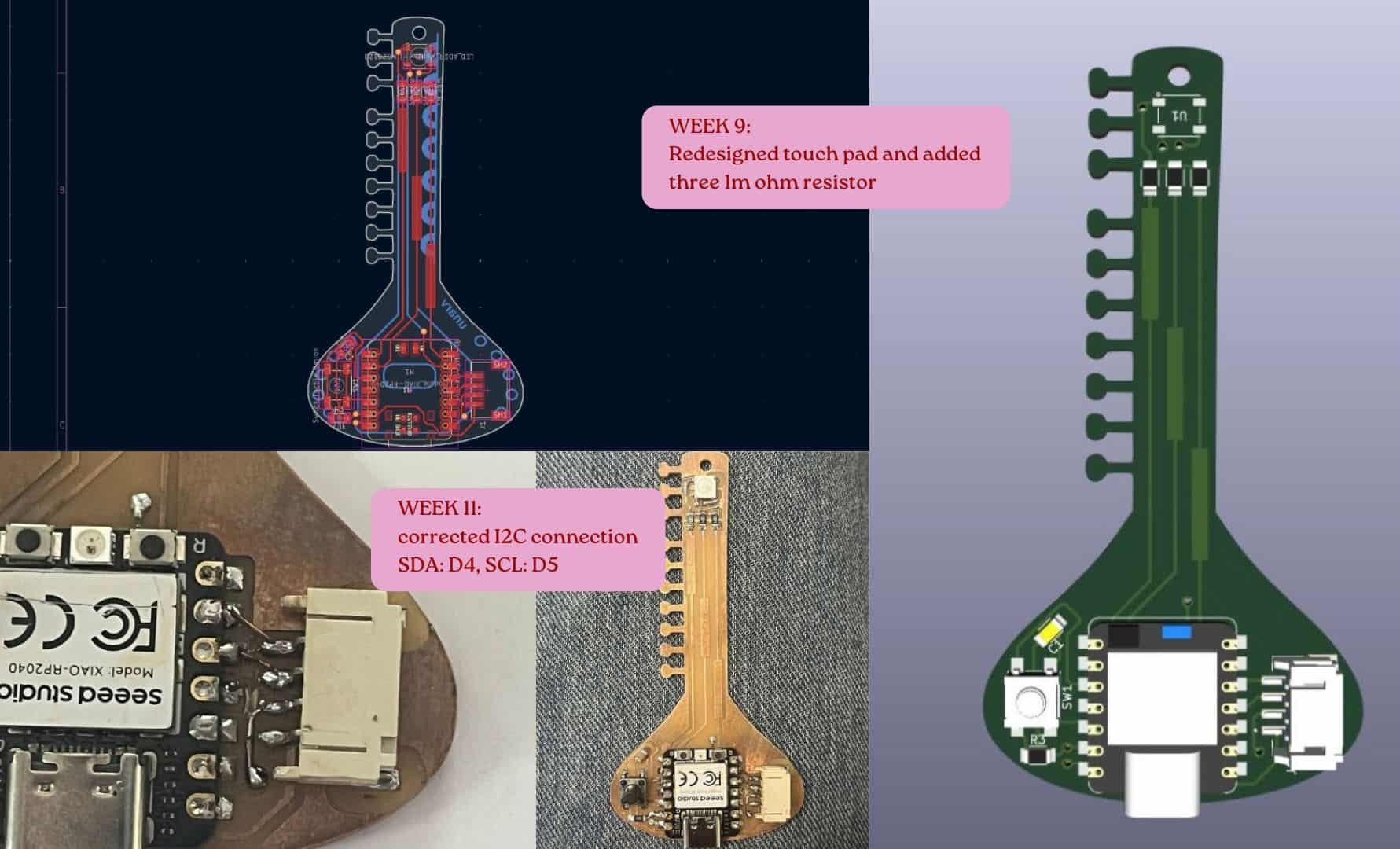
Week 9: Input device
During Input Devices, I updated the capacitive touch circuit by adding the required 1 MΩ resistor and modifying the touch pad spacing.
Week 11: Networking and Communications
Later, in Networking and Communications, I corrected the I²C pin connections by rerouting the traces using copper wire.
The detailed documentation about modifications and lessons learned are documented in that respective weeks.