Week 06 Electronics Design
This week focuses on learning the fundamentals of electronic components, circuit principles, and PCB design workflows. I will study how components such as resistors, capacitors, diodes, transistors, connectors, and microcontrollers function within circuits, and review key electrical concepts like voltage, current, and power. I will also learn to use Electronic Design Automation (EDA) tools to create schematics, simulate circuits, and prepare PCB layouts while following proper design rules for fabrication.
Objectives
assignment:-Use the test equipment in your lab to observe the operation of a microcontroller circuit board
Individual assignment:-Use an EDA tool to design a development board that uses parts from the inventory to interact and communicate with an embedded microcontroller extra credit: try another design workflow extra credit: design a case for it
Group Assignment
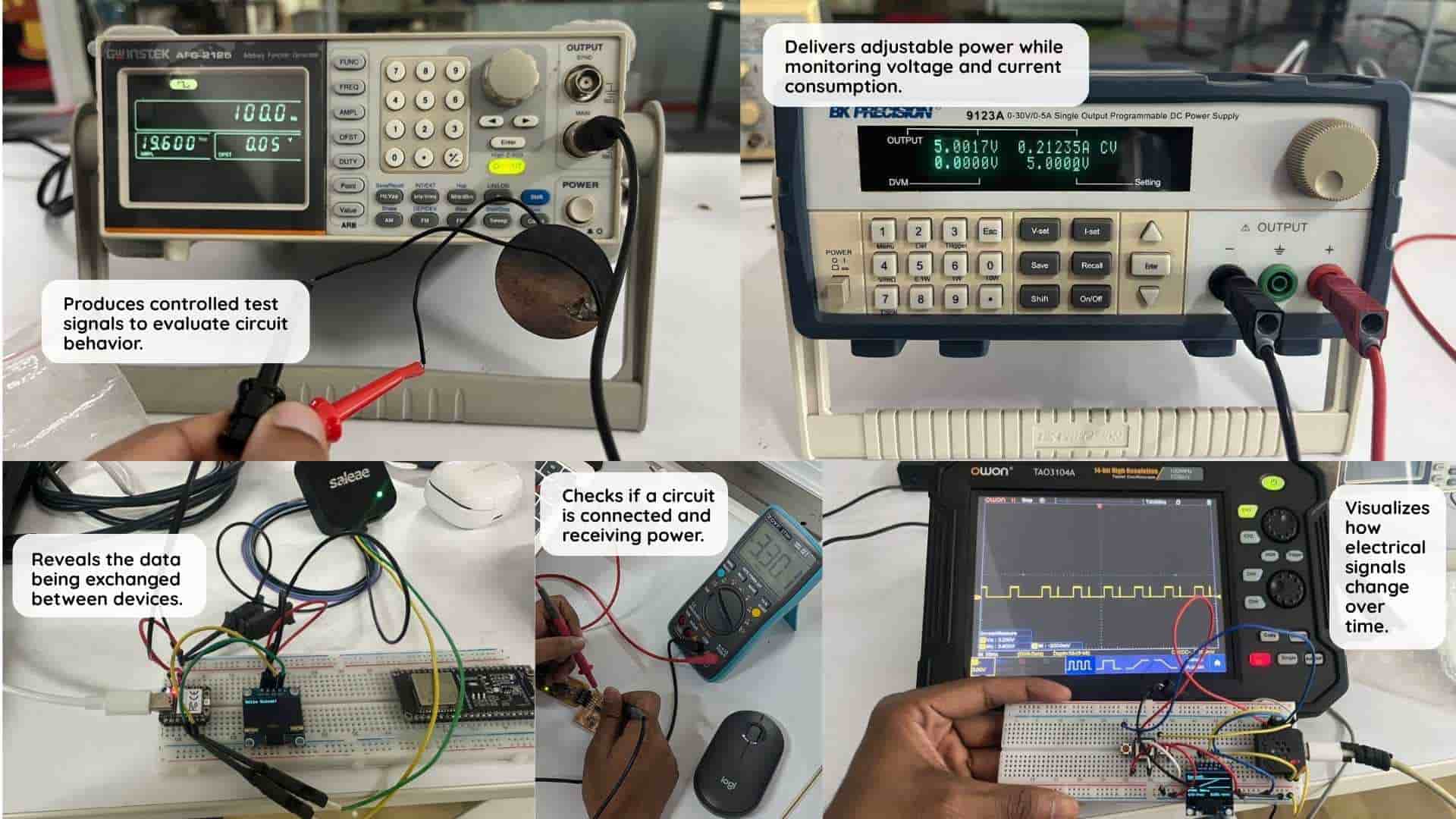
While the multimeter helped verify power, continuity, and component values, the oscilloscope made it possible to see how signals change over time. The logic analyzer provided a way to observe and decode communication between devices, and the function generator showed how different waveforms can be used to test electronic systems. The bench power supply highlighted the importance of supplying controlled power and setting safe current limits.
Together, these experiments showed that different tools reveal different parts of the same system, and choosing the right one makes troubleshooting much easier.
To know more, visitGroup Assignment.
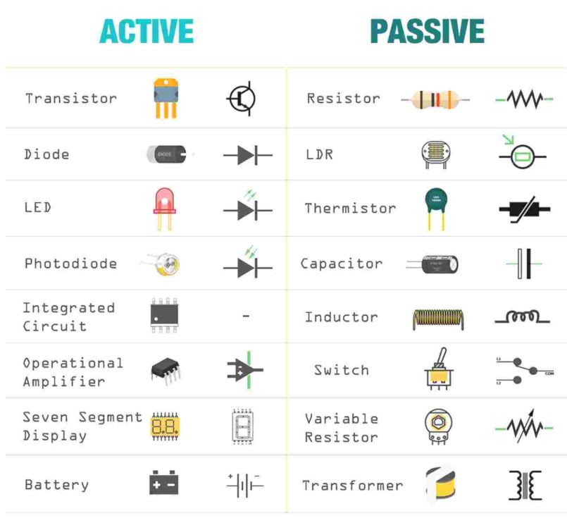
Electronic components
Electronic components are the fundamental building blocks of electronic circuits, designed to control the flow of electricity in a system. They can be active (such as transistors and diodes) or passive (such as resistors and capacitors), each serving a specific function within a circuit. When connected on a printed circuit board (PCB), these components work together to form functional electronic devices.
Active and passive components
Active and passive components are the two main types of electronic components used in circuits. Active components require an external power source to function and can amplify, switch, or generate electrical signals. Common examples include transistors, diodes, and operational amplifiers. In contrast, passive components do not need an external power source and mainly resist, store, or control the flow of electricity without amplification. Examples of passive components include resistors, capacitors, and inductors. Both active and passive components are essential for building and operating electronic circuits.
 Source.
Resistor
A resistor is a passive electronic component that limits or regulates the flow of electric current in a circuit. It is commonly used to control voltage levels, divide currents, and protect components from excessive current. Resistors are made from materials like carbon, metal film, or wire-wound ceramics, depending on their application. The resistance value is measured in Ohm (Ω). They come in different types, including fixed, variable (potentiometers), and surface-mount resistors (SMRs) for compact circuits.SMD (Surface Mount Device) resistors are small, flat components designed for direct mounting onto the surface of a PCB, making them ideal for compact, high-density circuits. In contrast, through-hole resistors have leads that pass through holes in the PCB and are soldered on the other side, providing strong mechanical bonds and easier handling.
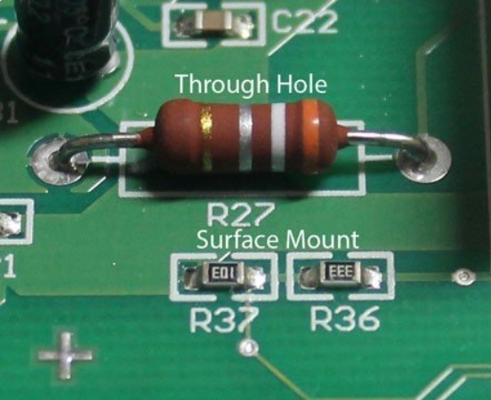 Image.
Capacitor
A capacitor consists of two or more parallel conductive plates that are electrically separated by an insulating material called the dielectric. These plates do not touch each other, and the dielectric can be made of air, waxed paper, mica, ceramic, plastic, or a liquid gel (as found in electrolytic capacitors). When connected to a voltage source, a capacitor stores electrical charge on its plates, creating an electric field between them. The ability of a capacitor to store charge is measured in farad (F), the SI unit of capacitance, where 1 farad (F) = 1 coulomb per volt (C/V). Since capacitors do not allow direct current (DC) to pass, they are widely used for energy storage, filtering, and signal processing in electronic circuits.
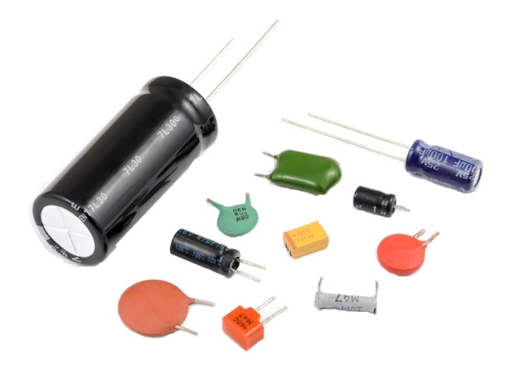 Image.
Inductor
An inductor is a passive electronic component that temporarily stores energy in a magnetic field when an electric current passes through its coil. It consists of two terminals and a coil of insulated wire, which can either loop through the air or wrap around a core material that strengthens the magnetic field. Inductors play a key role in managing fluctuations in electrical current within a circuit. The standard unit of inductance is the henry (H).
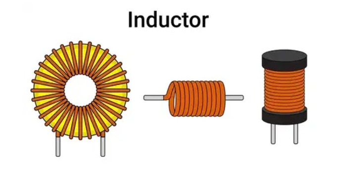 Image.
Transistor
A transistor is a semiconductor device that plays a vital role in amplifying or switching electronic signals and electrical power. It is composed of three layers of semiconductor material, where the flow of current or voltage between two layers is controlled by applying an electric current or voltage to the third layer. As a fundamental component in modern electronics, transistors are integral to the operation of devices such as radios, computers, and complex integrated circuits. They are available in different types, including bipolar junction transistors (BJTs), field-effect transistors (FETs), and MOSFETs, each designed for specific applications based on its distinct properties and working principles.
Diode
A diode is a semiconductor device that primarily allows current to flow in one direction while blocking it in the opposite direction. This property makes diodes essential for converting alternating current (AC) to direct current (DC), protecting circuits, and enabling various electronic functions.Diodes operate in two modes:
Types of Diodes
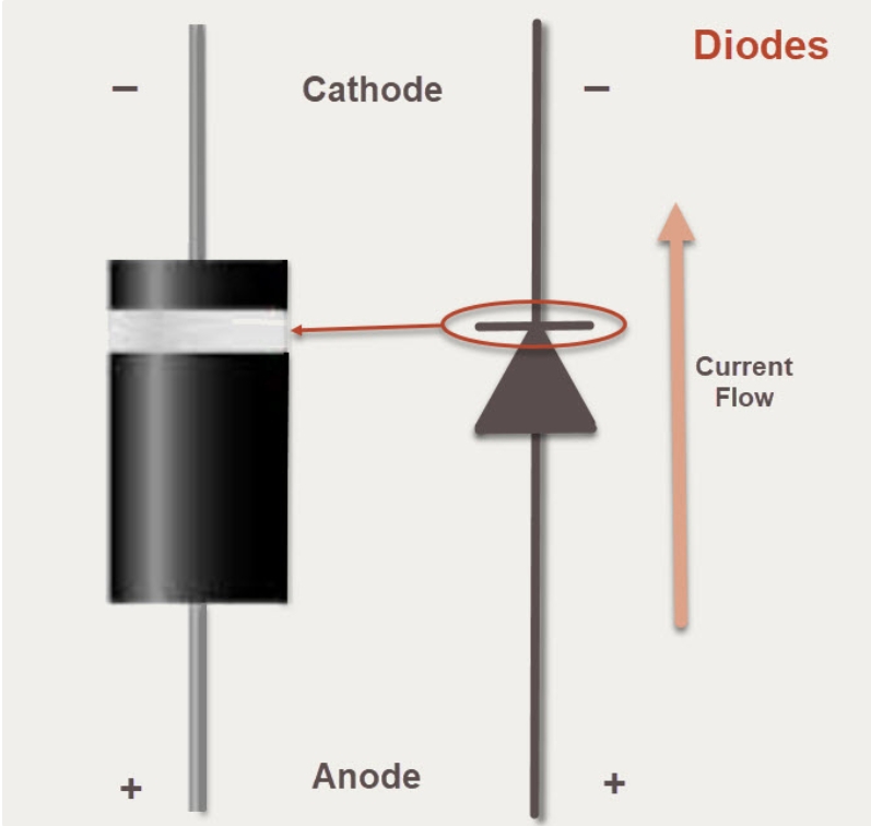 Image.
Integrated circuits (IC)
Integrated circuits (ICs) are essential components in modern electronics, consisting of resistors, capacitors, inductors, diodes, and transistors fabricated onto a single semiconductor chip, usually made of silicon. These components are interconnected to perform specific functions such as amplification, signal processing, computation, and power management. Since the semiconductor material is delicate, ICs are housed in protective plastic, ceramic, or metal packages with metal pins for easy connection to circuit boards. ICs can be categorized into analog, digital, and mixed-signal types, enabling compact, efficient, and reliable electronic devices.
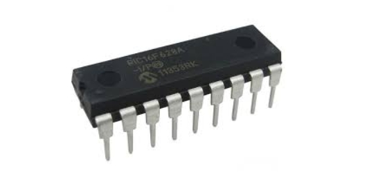 Image.
Switch
A switch is an electrical or electronic device that controls the flow of current in a circuit by connecting or disconnecting it. Switches can be broadly classified into mechanical and electronic (solid-state) switches. Mechanical switches, such as push buttons, toggles, and rotary switches, operate through physical movement and can be categorized based on actuation method, contact configuration, poles and throws, and operating states. Electronic switches, like transistors, MOSFETs, and thyristors, have no moving parts and use semiconductor technology to switch circuits efficiently, making them ideal for applications in automation, motor drives, and HVAC systems.
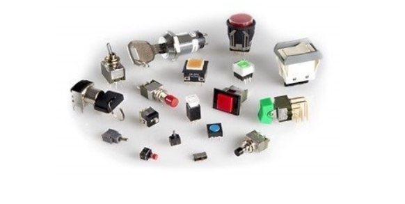 Image.
Wokwi
Wokwi.Wokwi is an online Electronics simulator. You can use it to simulate Arduino, ESP32, STM32, and many other popular boards, parts and sensors.
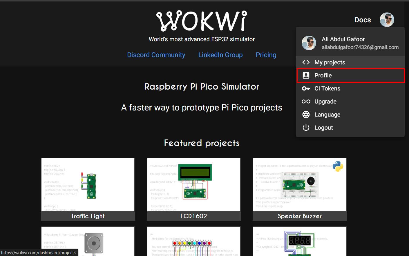
First, login to Wokwi
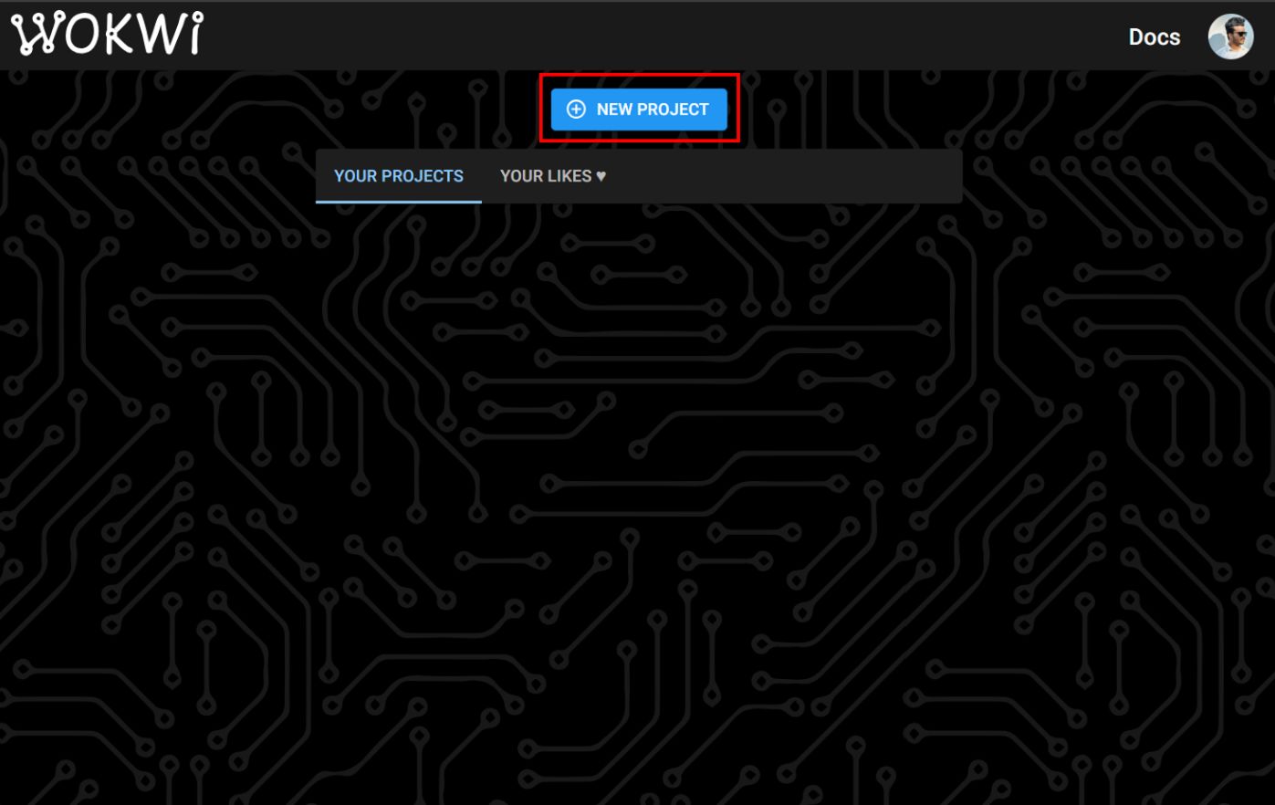
To begin the simulation process, I created a new project in Wokwi.
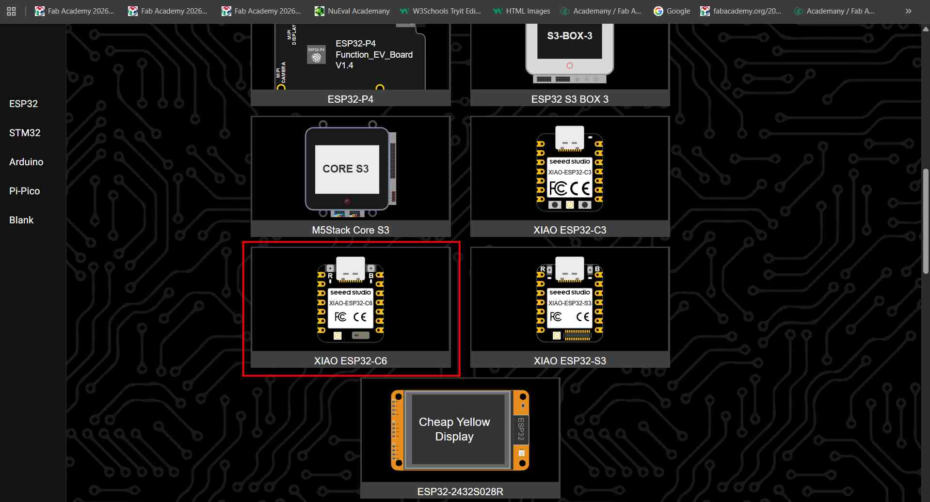
Next, I selected the XIAO ESP32 board in Wokwi to begin the simulation.
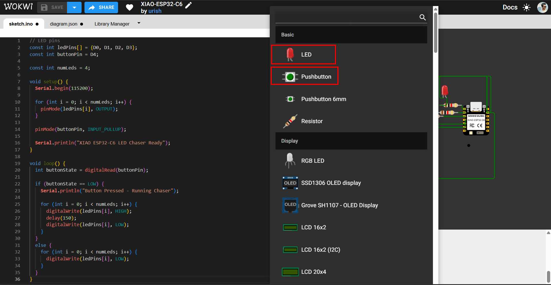
By using the 'Add' option in Wokwi, I included all the required components for the simulation
Next, I added the necessary components individually, including an LED, a resistor, and a push button.
Here are some commonly used shortcut keys in Wokwi:
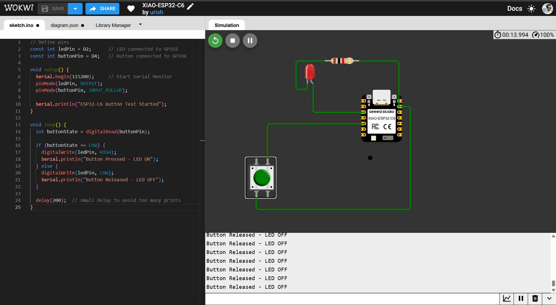
Internal pull-up function
An internal pull-up function refers to a feature in many microcontrollers, where a built-in resistor connects an input pin to the supply voltage (VCC). This internal pull-up resistor ensures that the input pin remains at a stable high logic level (HIGH) when no external component is connected, preventing the pin from "floating" and picking up electrical noise that could lead to unreliable or unpredictable behavior. When a device like a push button is connected between the input pin and ground (GND), pressing the button creates a path to ground, pulling the pin LOW and allowing the microcontroller to detect a clear state change. Enabling the internal pull-up in code (e.g., using pinMode(pin, INPUT_PULLUP) in Arduino) eliminates the need for an external resistor, simplifying circuit design and reducing component count.
I wrote a program to blink an led using push button
MicroPython is specifically tailored for microcontrollers and embedded devices, enabling developers to write Python code directly on low-power devices. The program code is given below. To comment a line we need to add "/" in the begining
// Define pins
const int ledPin = D2;      // LED connected to GPIO2
const int buttonPin = D4;   // Button connected to GPIO4

void setup() {
  pinMode(ledPin, OUTPUT);
  pinMode(buttonPin, INPUT_PULLUP);  // Enable internal pull-up
}

void loop() {
  int buttonState = digitalRead(buttonPin);

  // Button pressed = LOW (because of pull-up)
  if (buttonState == LOW) {
    digitalWrite(ledPin, HIGH);  // Turn LED ON
  } else {
    digitalWrite(ledPin, LOW);   // Turn LED OFF
  }
}
import machine
import time
It allows you to access and utilize functions, classes, and variables defined in external files, known as modules.
LED_PIN = D2
BUTTON_PIN = D4
led = machine.Pin(LED_PIN, machine.Pin.OUT)
button = machine.Pin(BUTTON_PIN, machine.Pin.IN, machine.Pin.PULL_UP)
The LED is connected to GPIO2.The button is connected to GPIO14 with an internal pull-up resistor, meaning
it reads high (1) when not pressed and low (0) when pressed.
while True:
if not button.value():
led.on()
print("LED ON!")
time.sleep(0.5)
else:
led.off()
print("LED OFF!")
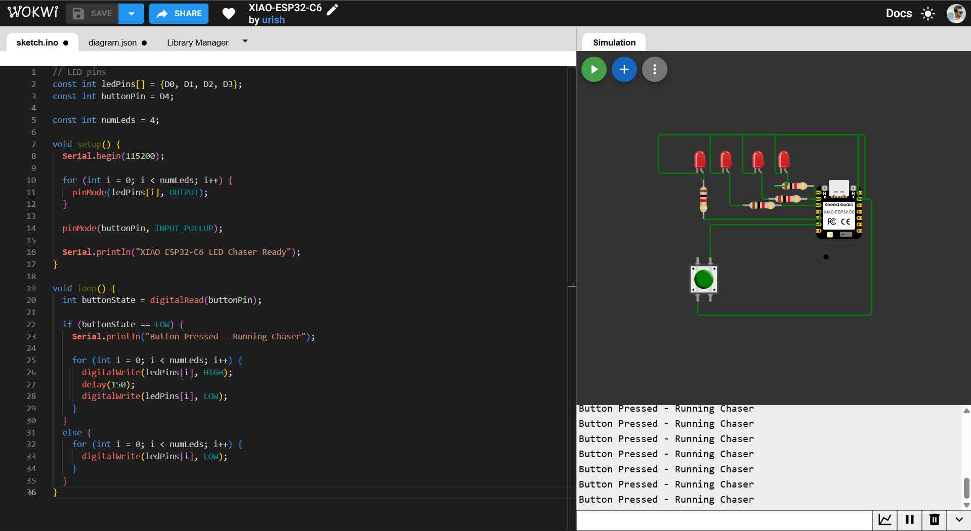
I wrote a program for Led chasser
I used chatgpt to refer the code.
promt:-How to code for Led chasser intensity using rp 2040
The program code is given below
// LED pins
const int ledPins[] = {D0, D1, D2, D3};
const int buttonPin = D4;

const int numLeds = 4;

void setup() {
  Serial.begin(115200);

  for (int i = 0; i < numLeds; i++) {
    pinMode(ledPins[i], OUTPUT);
  }

  pinMode(buttonPin, INPUT_PULLUP);

  Serial.println("XIAO ESP32-C6 LED Chaser Ready");
}

void loop() {
  int buttonState = digitalRead(buttonPin);

  if (buttonState == LOW) {
    Serial.println("Button Pressed - Running Chaser");

    for (int i = 0; i < numLeds; i++) {
      digitalWrite(ledPins[i], HIGH);
      delay(150);
      digitalWrite(ledPins[i], LOW);
    }
  }
  else {
    for (int i = 0; i < numLeds; i++) {
      digitalWrite(ledPins[i], LOW);
    }
  }
}
Key Translation Details:
Defines constant integer for button and LED connected these are addressed directly by their GPIO numbers (0, 1, 2, 3, and 4).
void setup() { pinMode(buttonPin, INPUT_PULLUP); pinMode(ledPin, OUTPUT); Serial.begin(115200); }
setup() function runs once the ardino is powered on/ reset.Button pin defines pin D4 as input. INPUT_PULLUP enables internal pull up resistor,which keeps the pin value high when the button is not pressed ledPin defines pin D0,D1,D2,D3D4 as output. In Serial.begin(115200) serial communication begins at 115200 bits per second.
KiCad
KiCad is a free, open-source Electronic Design Automation (EDA) software suite used for creating schematics and designing printed circuit boards (PCBs). It provides tools for schematic capture, PCB layout, circuit simulation, and generating manufacturing files such as Gerber files. KiCad also includes features like 3D modeling, bill of materials (BOM) generation, and engineering calculations, making it a powerful tool for electronics design.
Go to the official KiCad website - . Choose your operating system (Windows, macOS, or Linux). Download the installer for the latest stable version.Run the installer and follow the installation instructions.I downloaded and installed KiCad. Now open KiCad . File → New Project . Name your project
Downloaing Fab Academy KiCad library
We installed the Fab Academy KiCad library from:KiCAD Library.
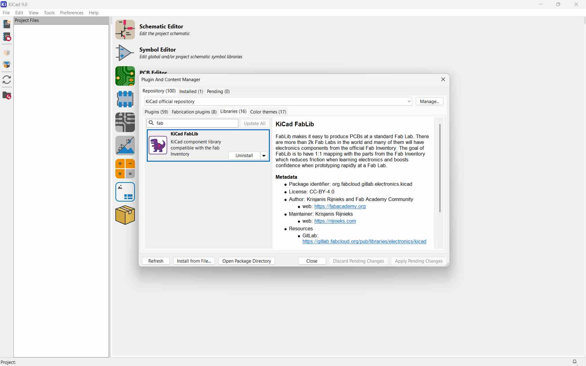
installing and configuring the library
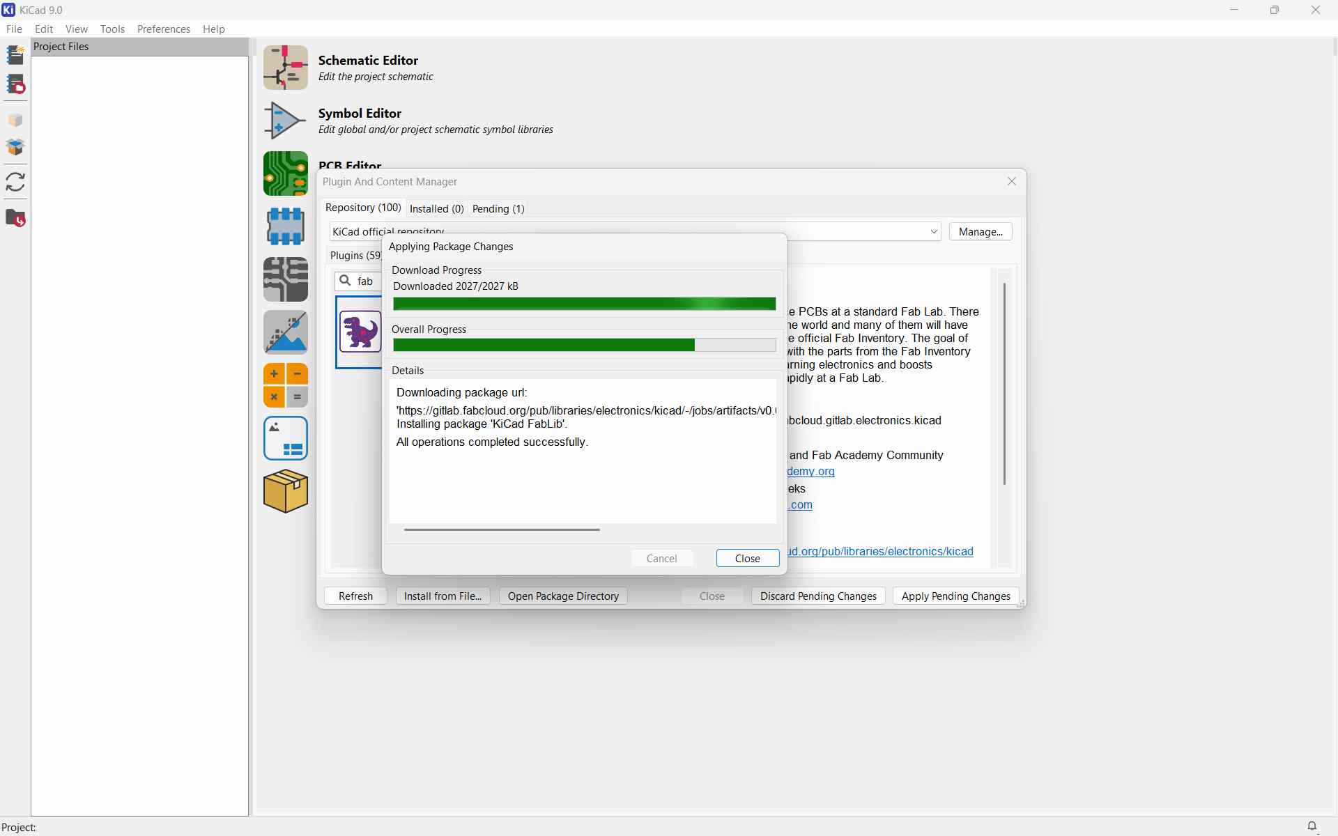
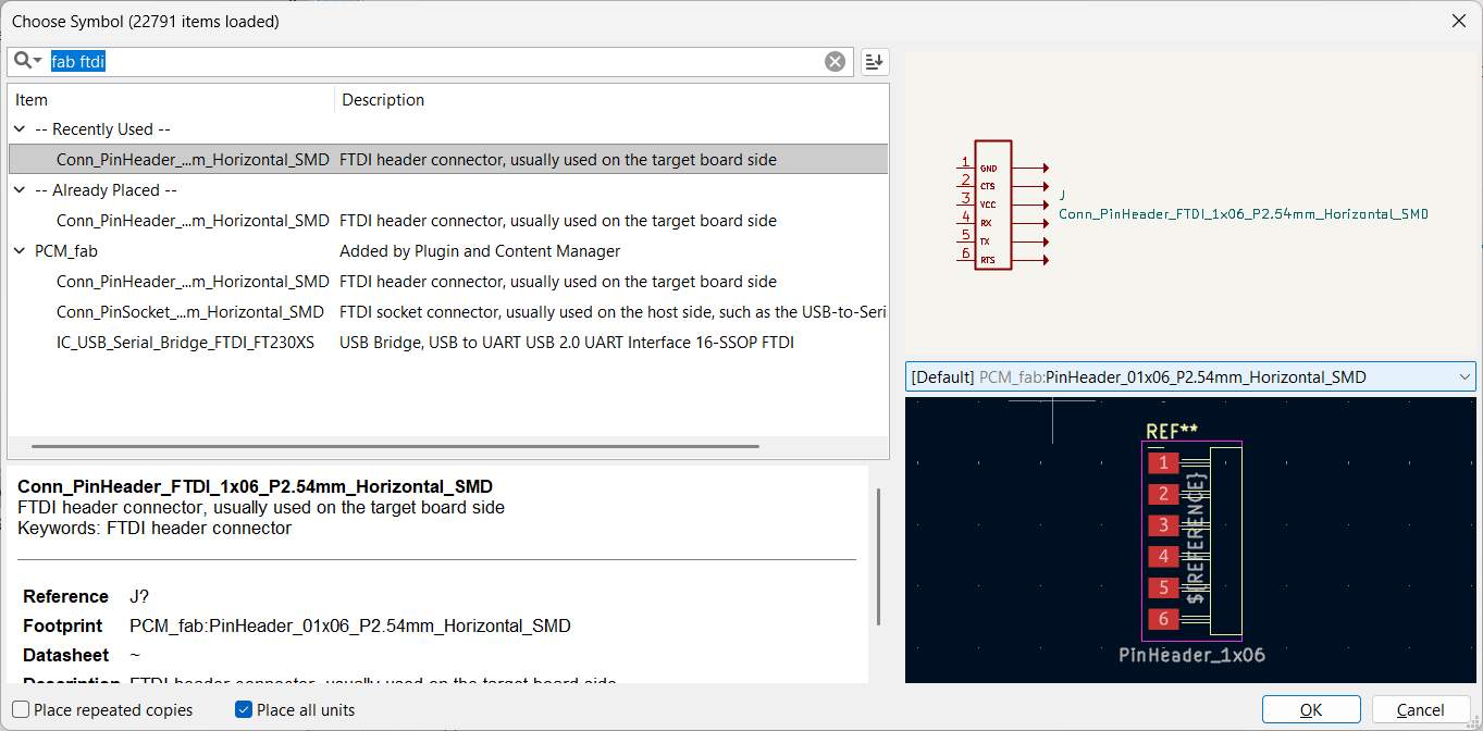
After installing and configuring the library, components from this collection appeared with the prefix “fab” in the search results. These libraries contain footprints and symbols specifically prepared for digital fabrication workflows.
Component search results showing Fab library symbols.
Custom PCB Design - Individual Assignment
Design 1
Before adding components to my design, I referred toFabStash -FabStash - a website listing all components available in the Super Fab Lab Kochi inventory and reviewed the relevant datasheets
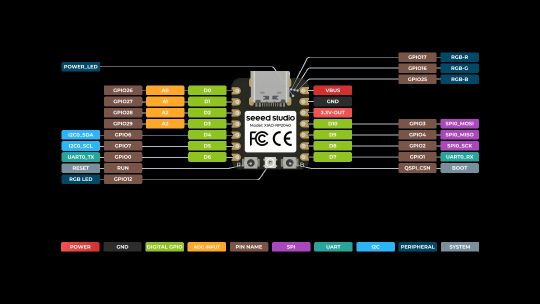
XIAO-RP204
this week iam using XIAO RP2040
 Source
Snap Magic
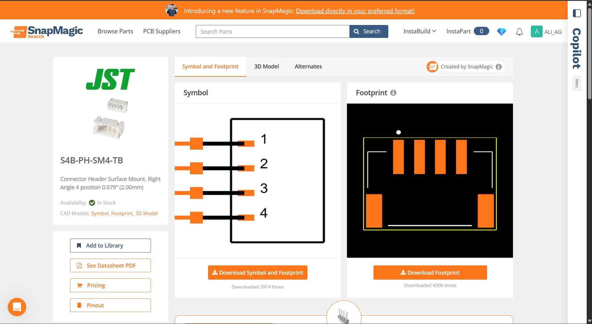
Snap Magic - . is a free online platform that provides schematic symbols and PCB footprints compatible with KiCad
Since the required microcontroller was not available in the default KiCad library, I searched for it in Snap Magic. I downloaded the KiCad files, extracted the ZIP file, and added the symbol and footprint to my project.
The pin configuration was verified using the datasheet to ensure correct connections.
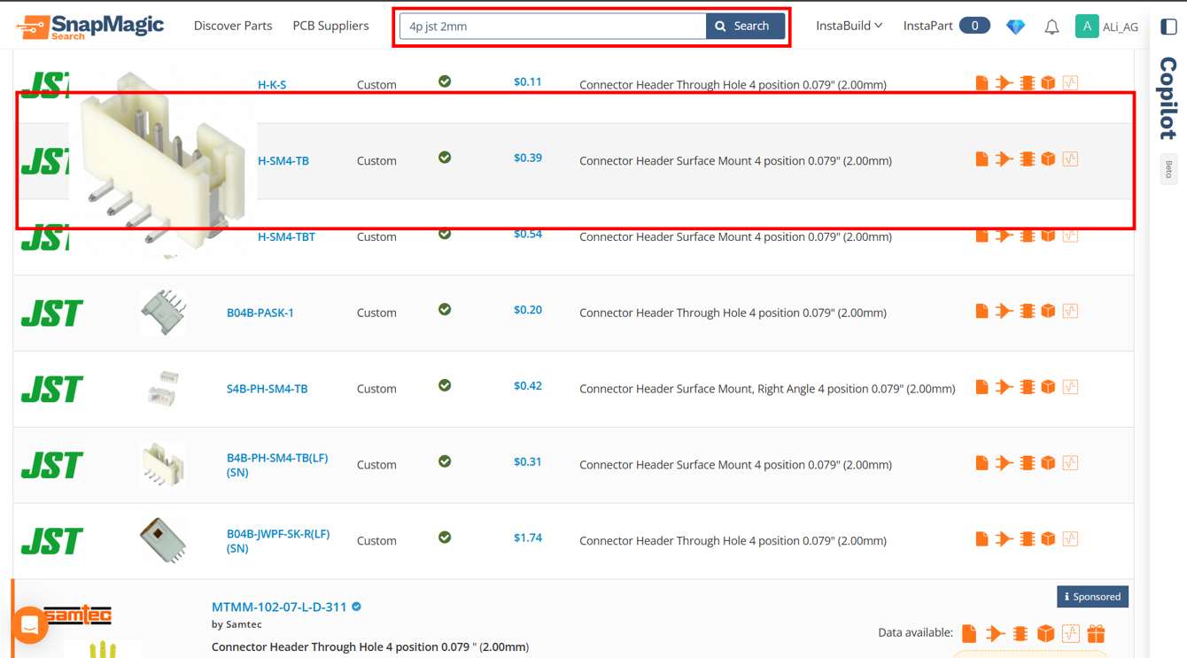
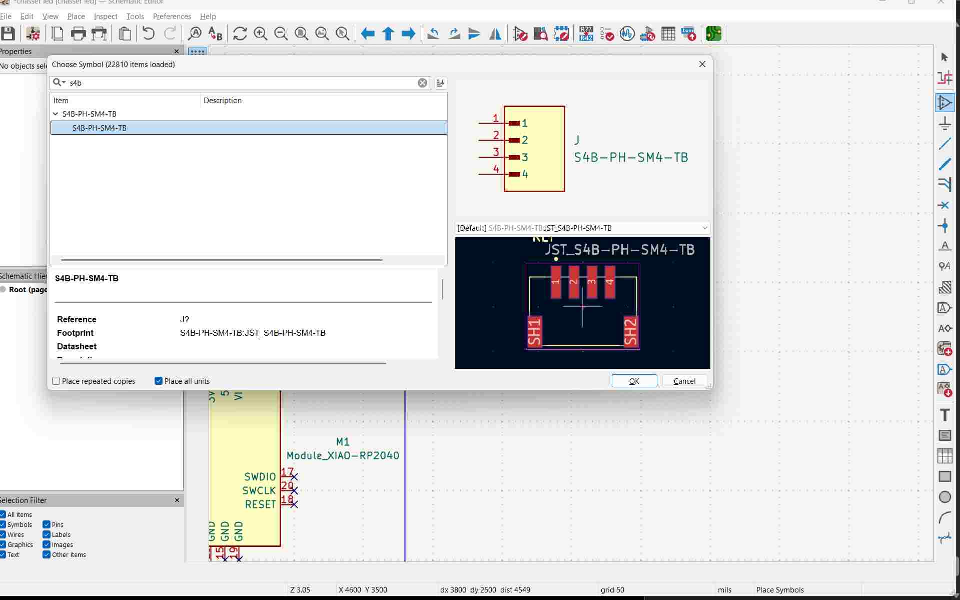
I used Snap Magic to find a 2.0 mm pitch, 4-position, right-angle surface-mount header connector. Since it was not available in the default KiCad library, I downloaded the symbol and footprint from Snap Magic and added them to my project.
After selecting the component I needed, I downloaded the KiCad symbol and footprint files for use in my project
Next, select the required PCB software format (e.g., KiCad) before downloading the files.
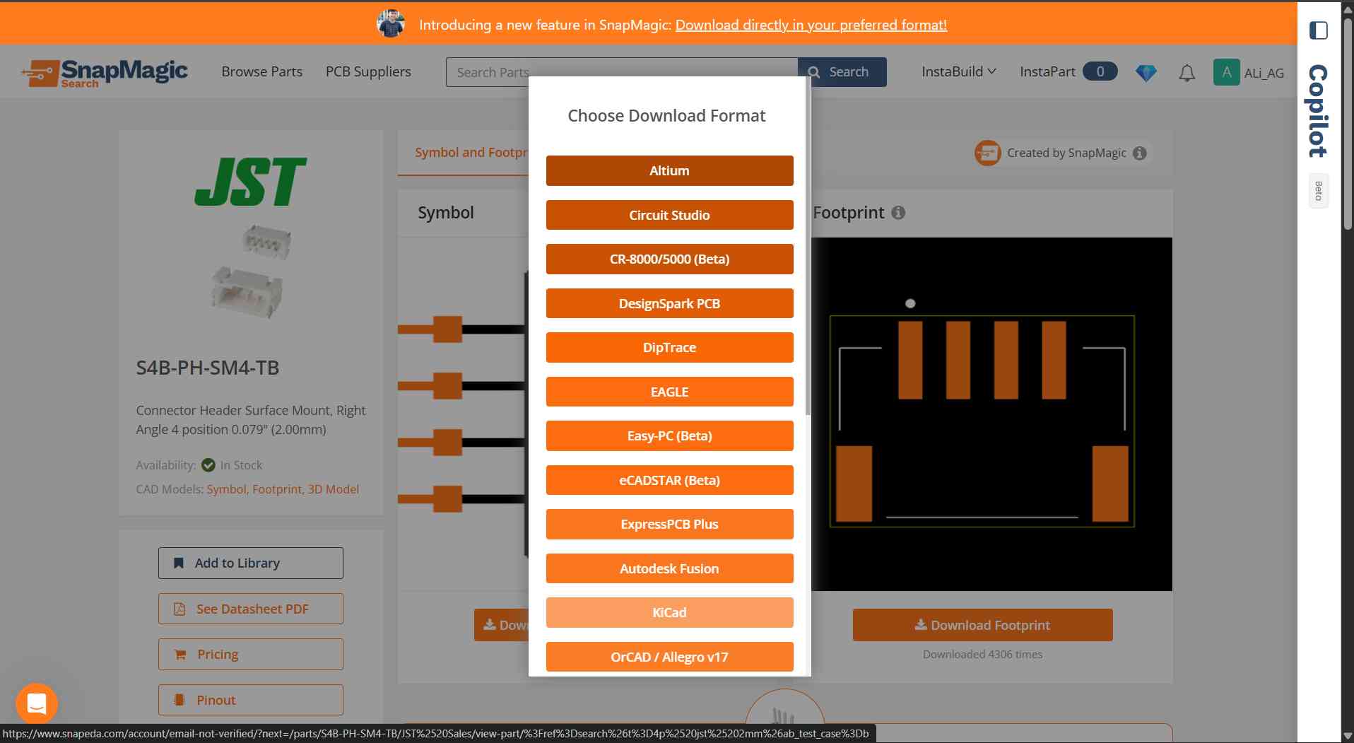
After selecting the software format, you will receive three file format options, such as symbol, footprint, and 3D model (STL).
Next, go to the Preferences menu in KiCad to add the downloaded symbol and footprint libraries.
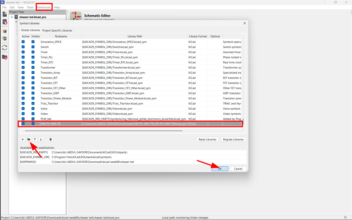
Select the required library file and load it into KiCad.
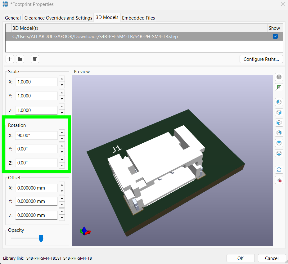
Open Footprint Properties and add th Step file, press E or Right-click >> Properties >> Footprint Properties >> 3D Models tab >> 3D Shape >> Browse the .step or .stp file >> Click OK
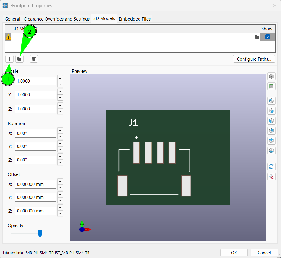
Select 3d model
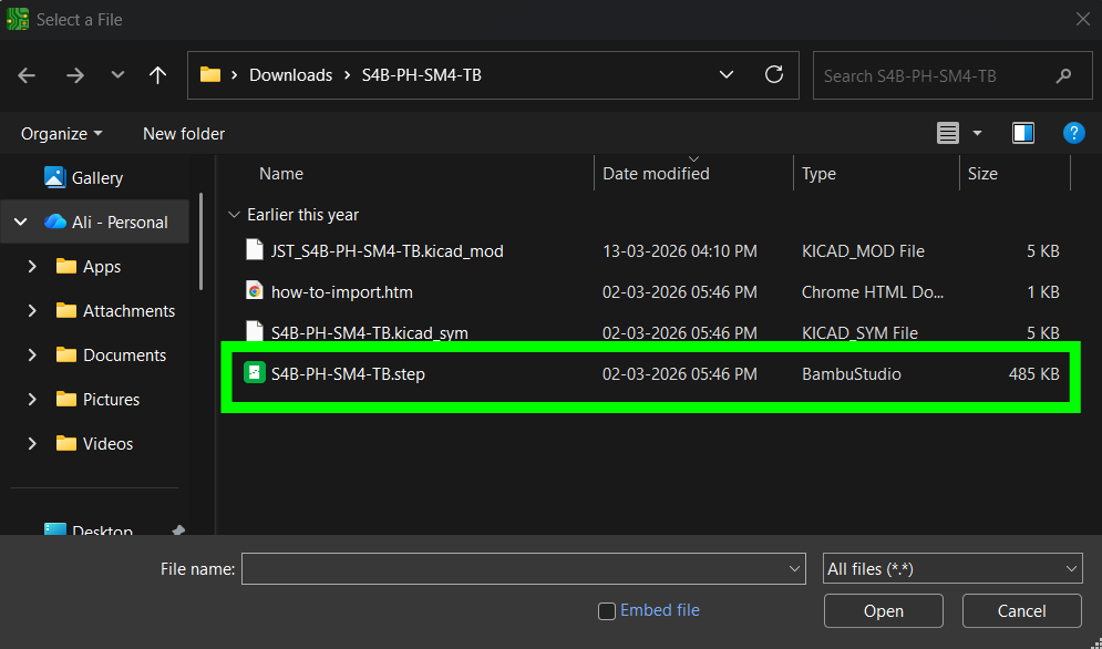
Make propper oriantation and position
connecting two symbols using wire
Select wire tool in kicad
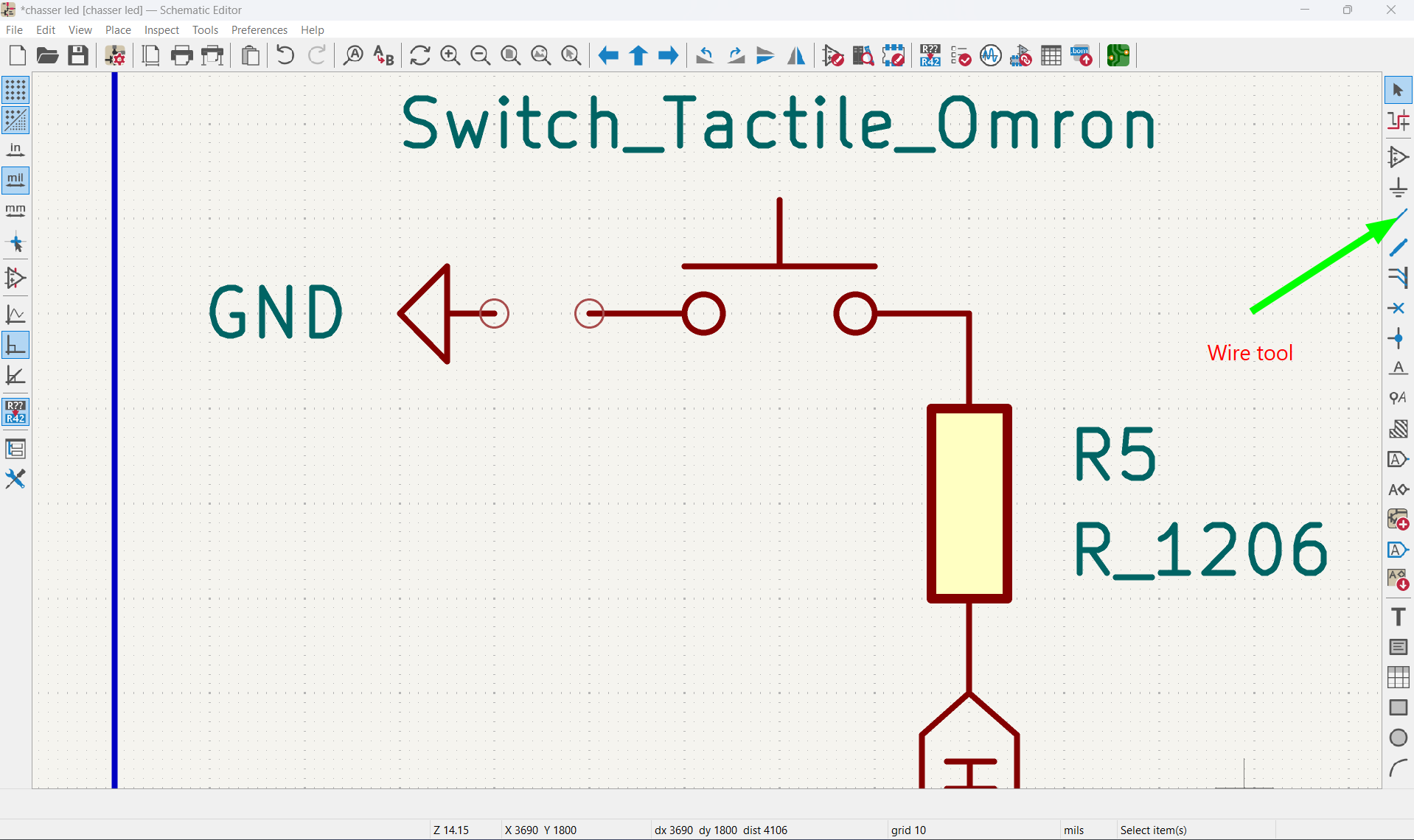
using kicad wire tool by drawing wires between the component point
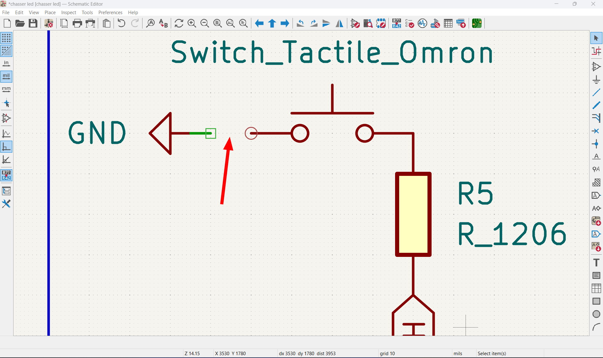
after drawing the wire
Resistor calculation
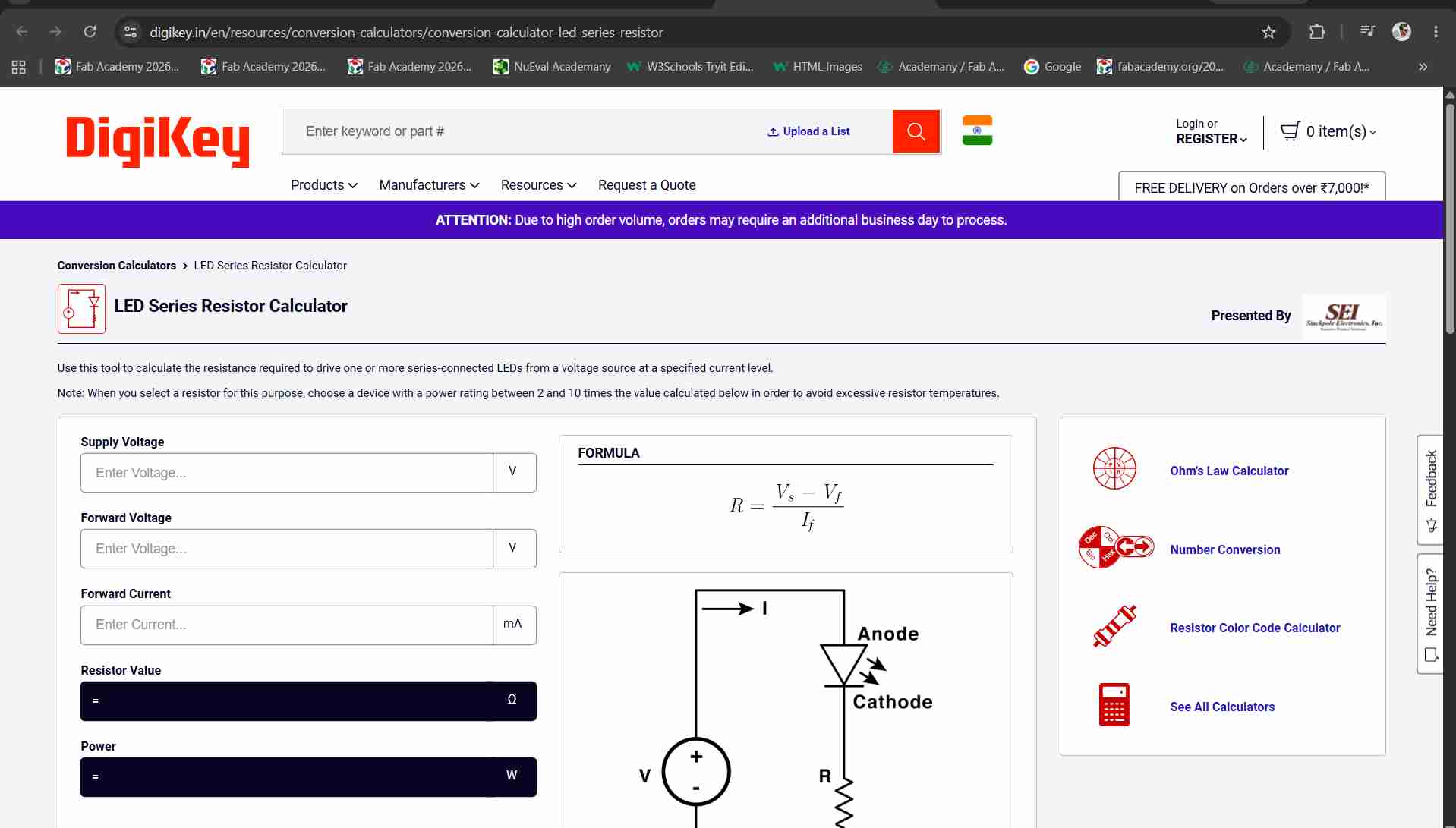
I used this website to calculate the resistor value for the LED LED Resistor Calculator
Using Global Labels for Clean Connections
To avoid excessive wire crossings and improve readability, we used the Place Global Label tool. Labels allow connections between components without drawing long physical wires, making the schematic cleaner and easier to understand.
click on global label and there you can add name you want
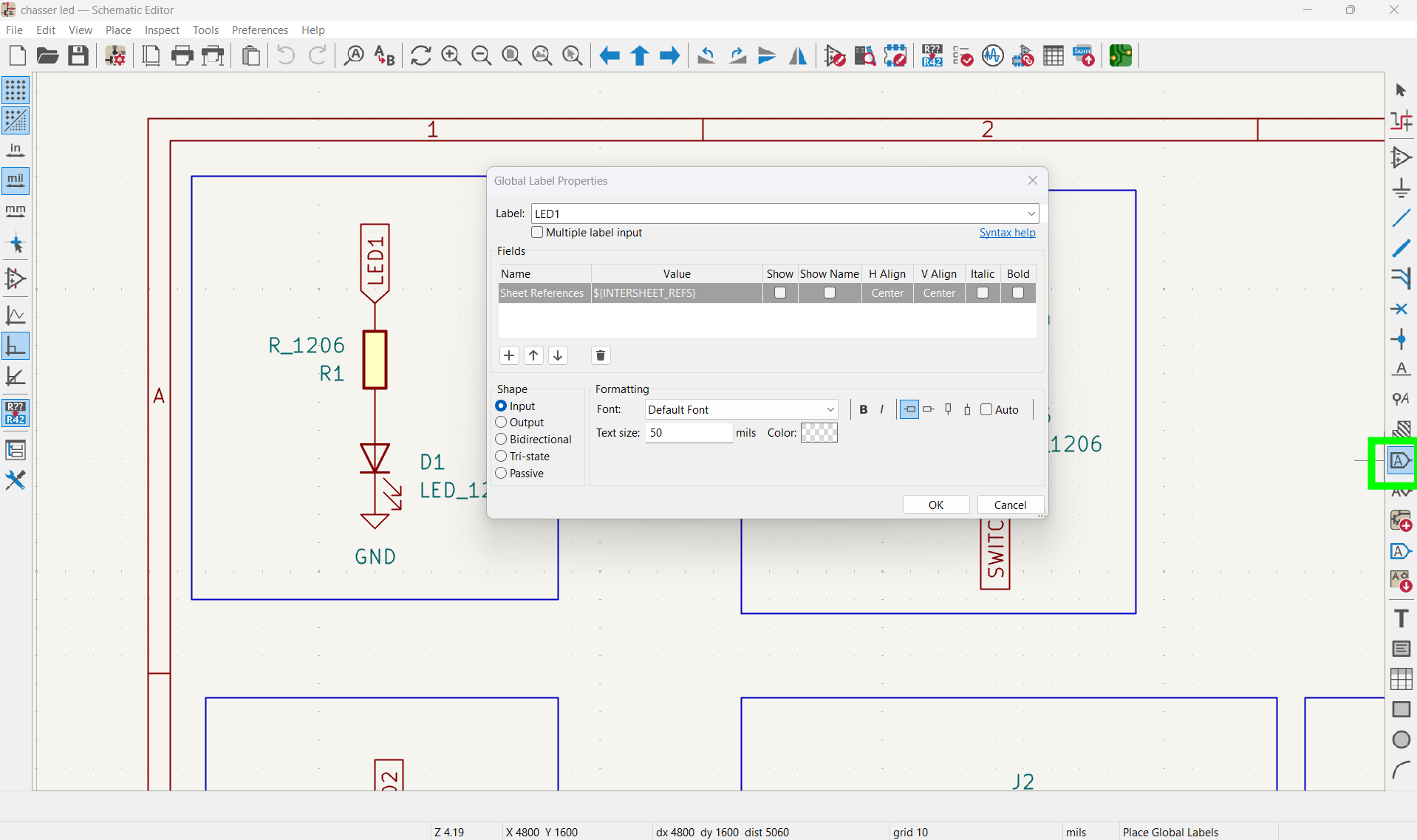
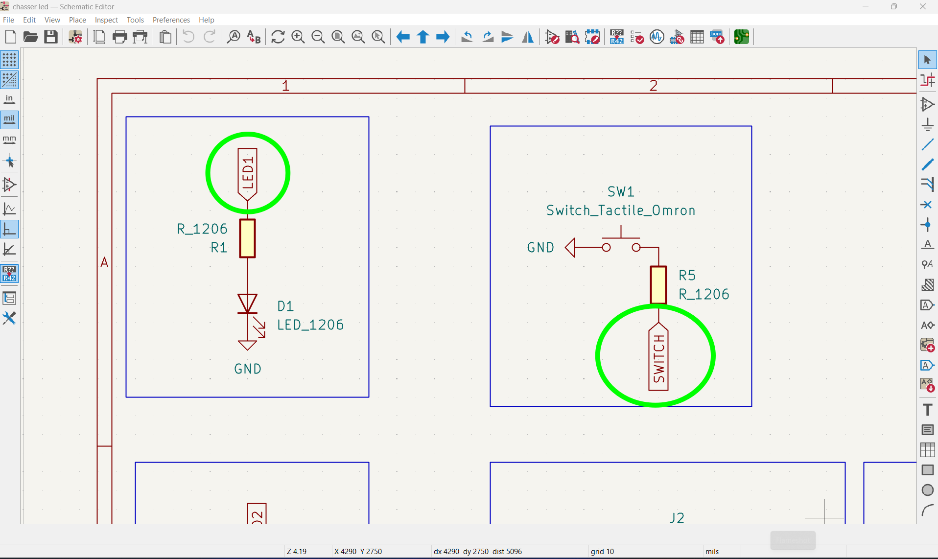
Diagram with label
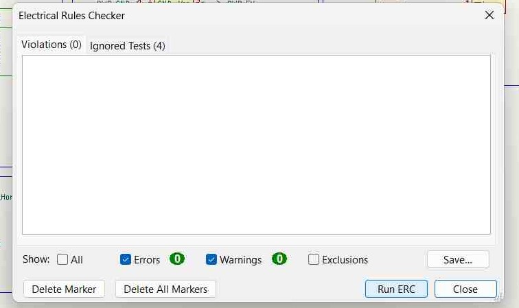
Electronical Rules Checker (ERC)
Check ERC for errors and correct them before moving onto PCB Editor.
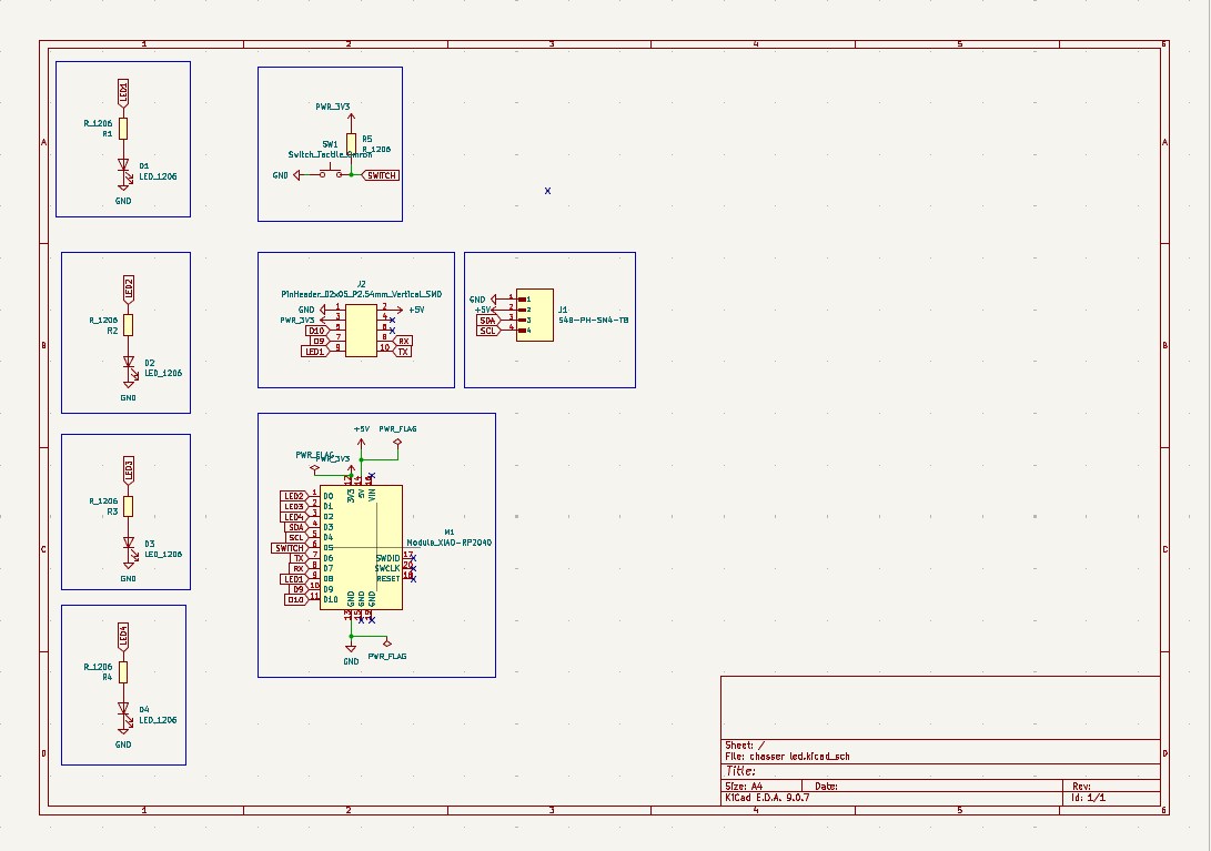
Schematic editor
Instructor Saheen demonstrated how to use KiCad for PCB design with a practical example. We followed along using the component values and design specifications provided by him. In KiCad we have two editors, schematic editor and pcb editor. Open schematic editor.
.jpeg)
Add Components
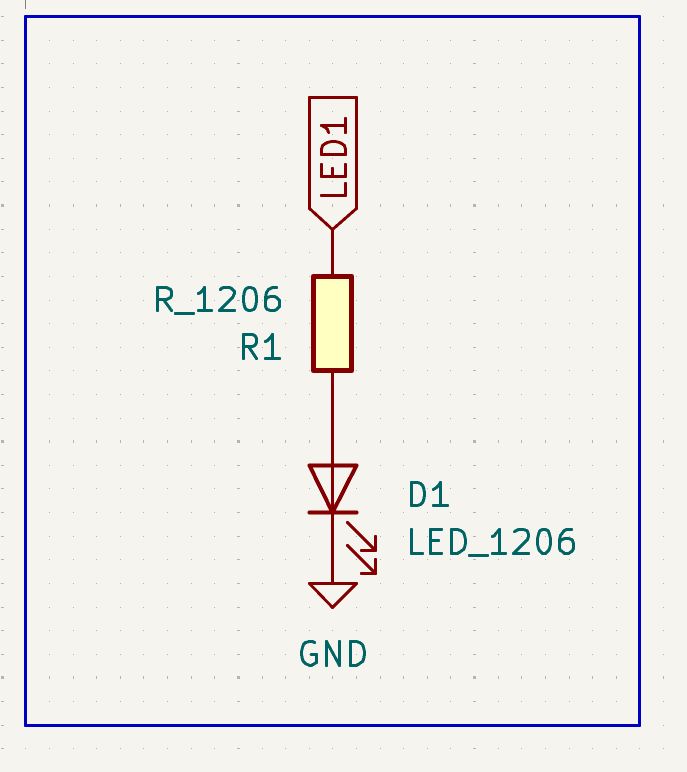
LED
I placed a red LED in my circuit and powered it with 5 V. I added a 220 Ω resistor in series with the LED to limit the current flowing through it. Without the resistor, the LED could have drawn too much current, potentially damaging itself or the microcontroller. The resistor ensured that the LED operated safely within its current rating, providing stable and reliable illumination. For a standard red LED, the forward voltage is usually around 2 V, and the safe operating current is about 20 mA. so the voltage that needs to drop across the resistor is 3so the voltage that needs to drop across the resistor is 3V. From ohm's law the value of resistor found to be 150 ohm. And we use 220 ohm as standard.
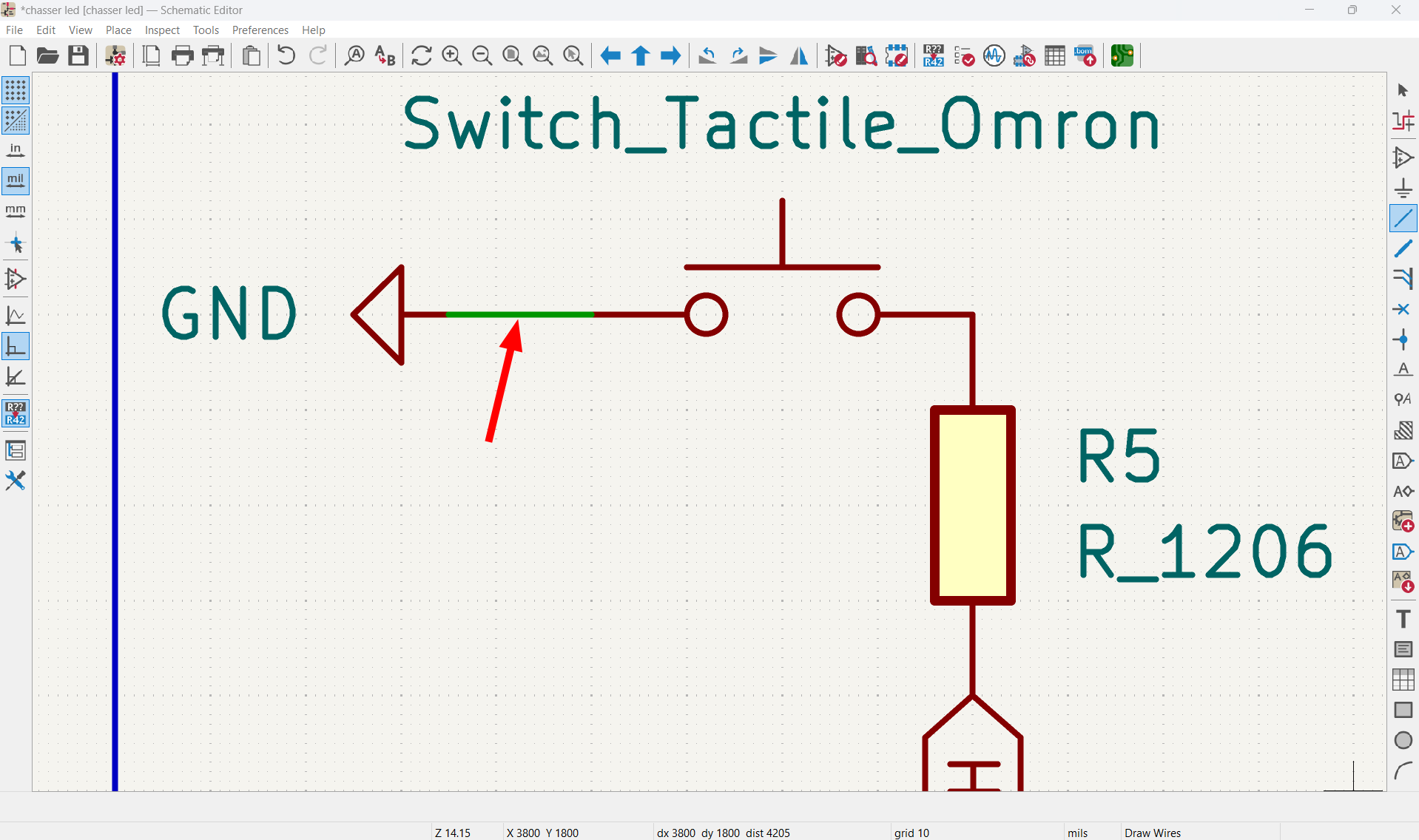
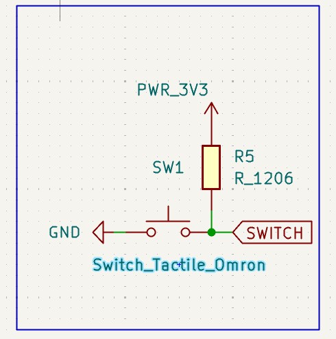
Switch
I added a switch to my circuit and connected a resistor between the input pin and 5 V, which made it a pull-up resistor configuration. When the switch was open, the resistor kept the pin at a HIGH state (5 V). When I pressed the switch, it connected the pin to ground, pulling it LOW. The resistor was important because it prevented the pin from floating when the switch was not pressed, ensuring stable and reliable digital readings.
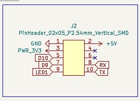
pin header connector
This is the schematic symbol of a 2×5 pin header connector (J2) showing power, ground, and signal connections such as D10, D9, RX, and TX.
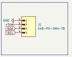
JST connector
This is the schematic symbol of a 4-pin JST connector (J1 – S4B-PH-SM4-TB) used for I2C communication, showing GND, +5V, SDA, and SCL connections.
This is final schematic Diagram
Add Power Symbols
Add Values and Labels
Transferring the Design to the PCB Editor
Next, switch to the PCB Editor. At the top toolbar, click the "Update PCB from Schematic" icon to import the latest schematic changes into the PCB layout. Unfortunately, I forgot to take a screenshot of this step.
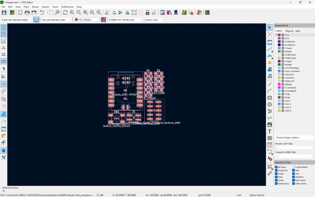
I arranged all components and conformed all path are ok for routeing
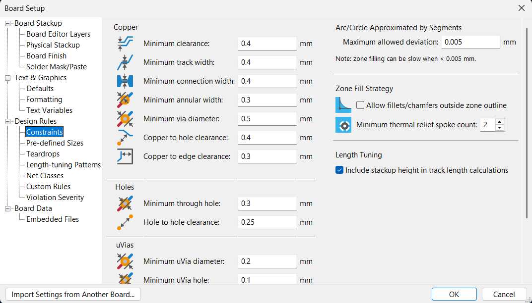
Configuring Design Rules
Before routing the PCB, I configured the design rules in KiCad to match the manufacturing constraints of the milling process. The values for minimum track width, clearance, and other parameters were based on the recommendations provided by our instructor. Setting these limits early helps prevent routing errors and ensures that the board can be manufactured reliably.
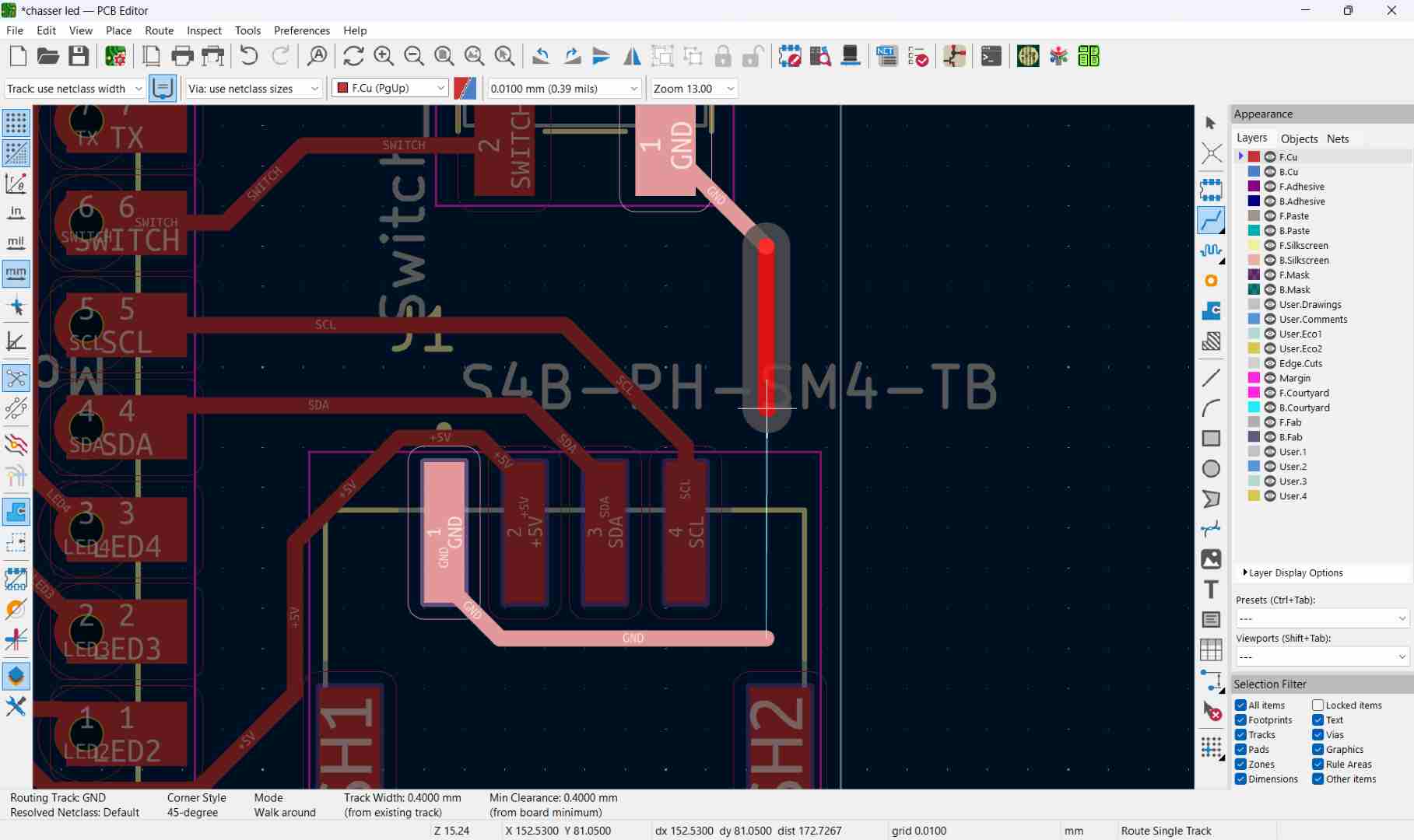
Route track
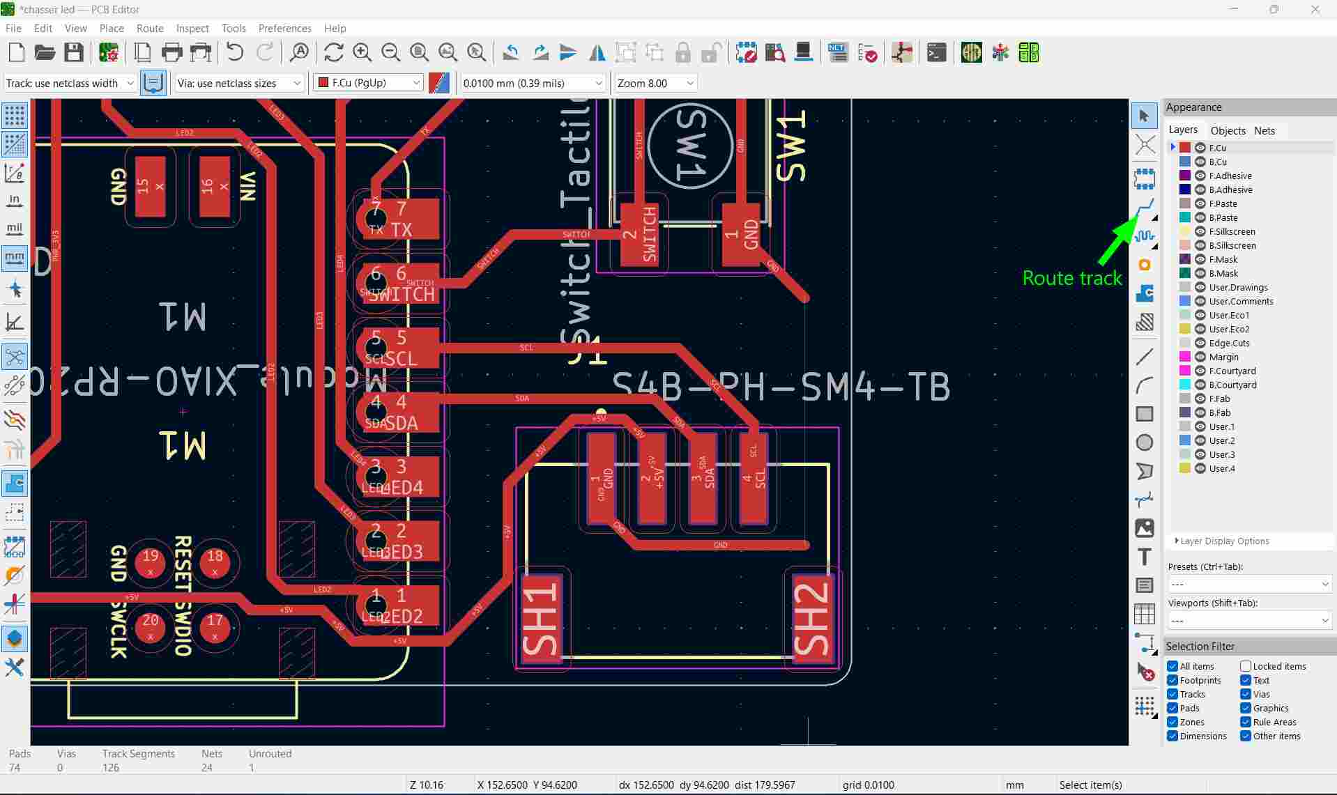
I used KiCad's Route Tracks tool to connect the PCB traces by following the airwires. The red trace shows the track being routed, and the airwire disappears automatically once the connection is completed.
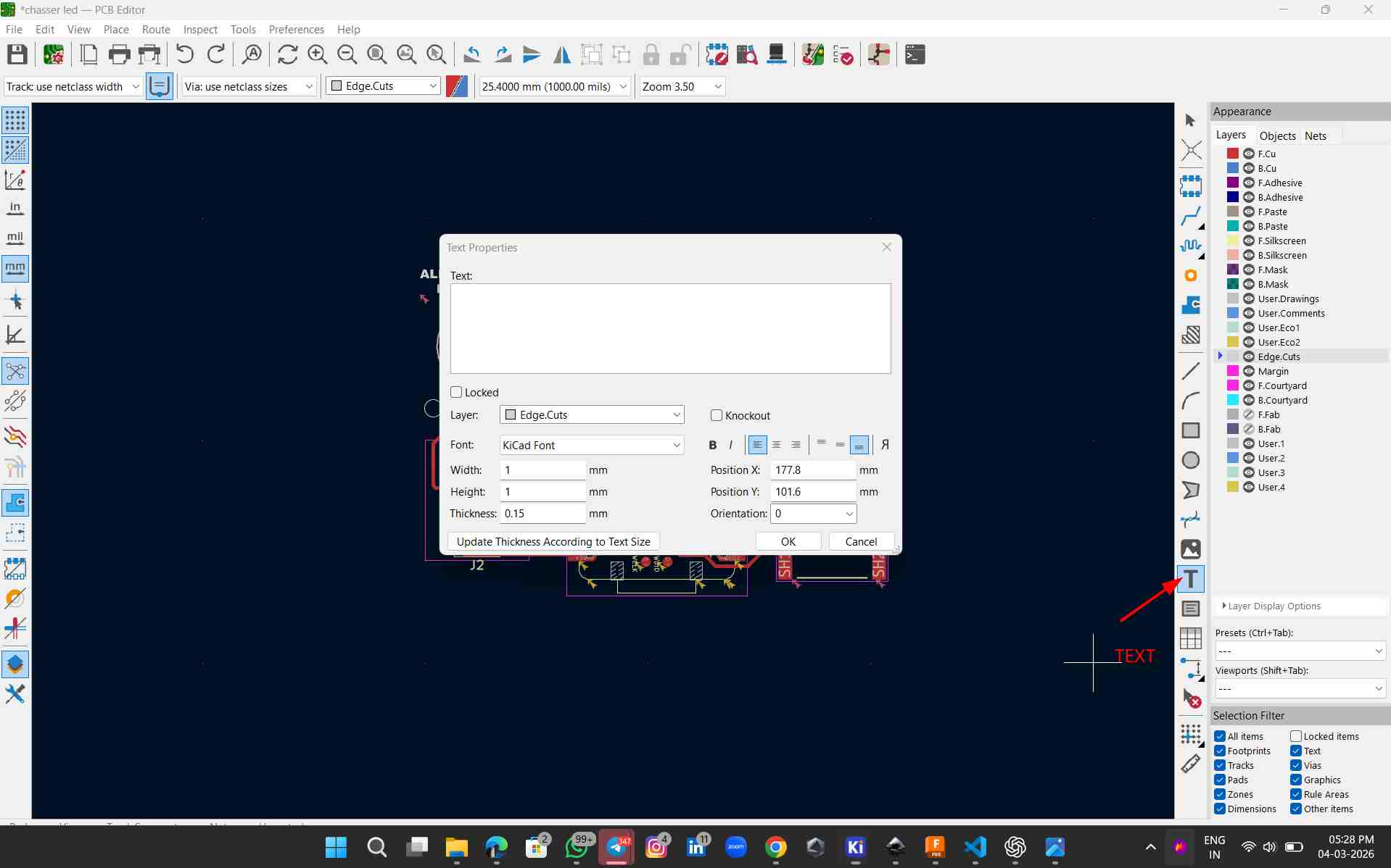
This image shows the Text Properties window in the PCB Editor of KiCad.
What is happening here
Important options in this window
✅ This tool is used to add labels, names, logos, or board information on the PCB design.
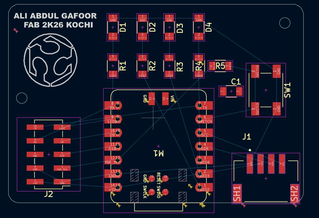
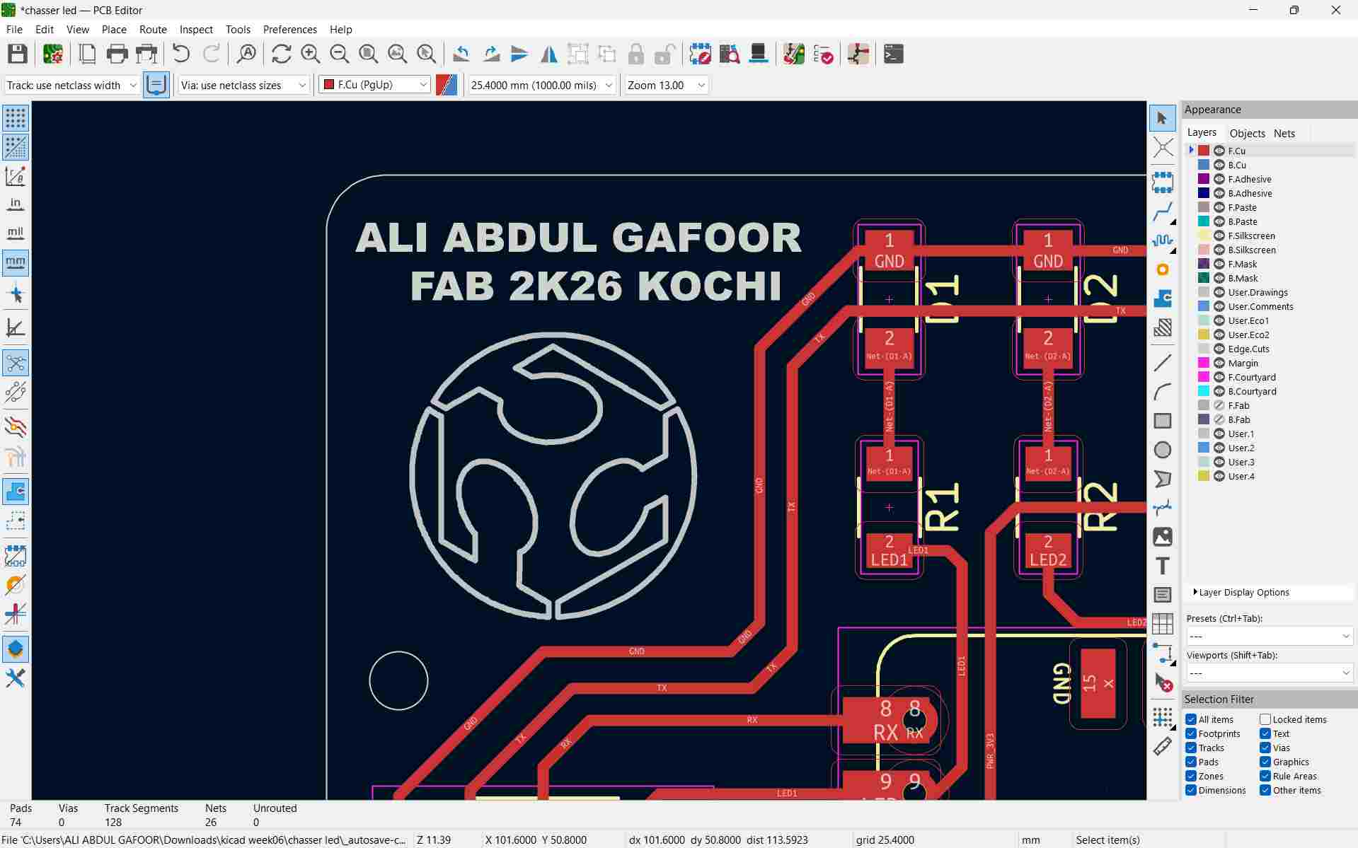
To add the logo on the PCB, I used Inkscape. I imported the Fab logo, then used the Bitmap Trace tool to convert the image into a vector. After that, I exported the design as a DXF file and imported it into KiCad.
This is the same process we used in Week 02 to convert images into vector format for use in design.
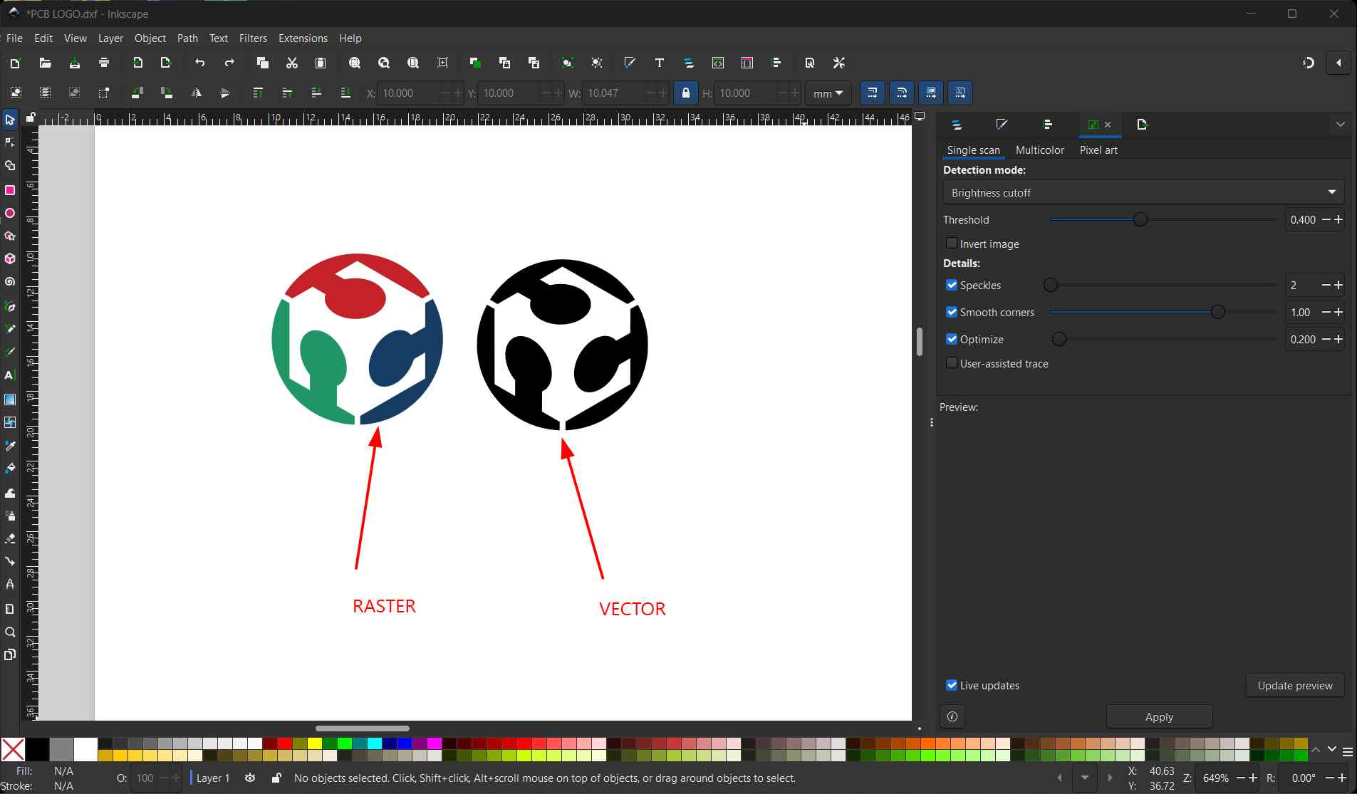
To add an image to the PCB, go to File → Import → Import Graphics in KiCad. Then select the DXF file, import it, and set the required dimensions/scale before placing the image on the PCB.
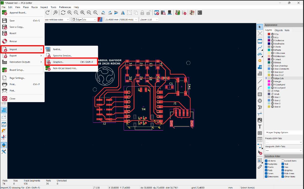
After importing the DXF file, I used the Ctrl (Control) key to place and adjust the position of the logo on the PCB. This allowed me to move the imported Fab logo to the correct location on the board in KiCad.
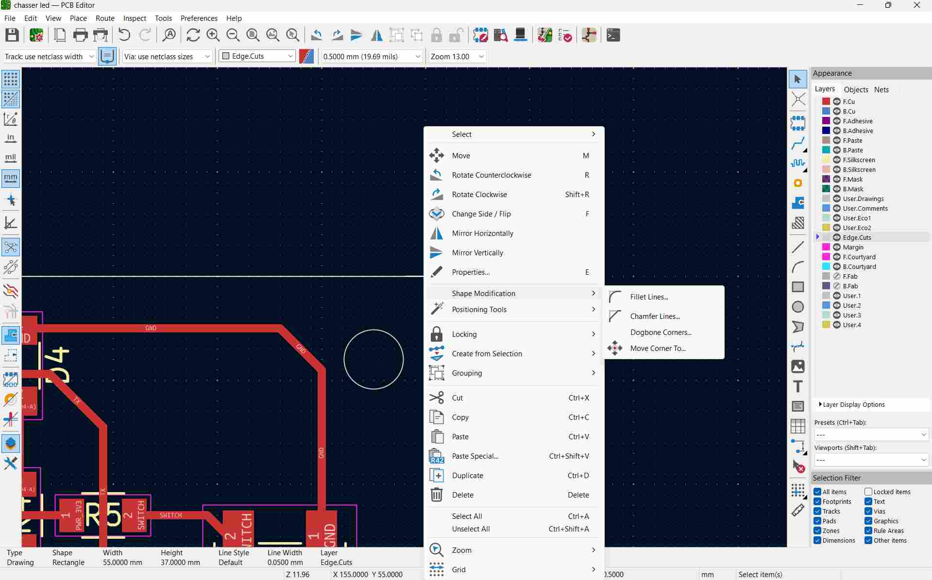
I gave a fillet to the outer edges of the PCB by right-clicking the edge and selecting the fillet option in KiCad.
After completing the design, I checked the DRC (Design Rule Check) in KiCad, and there were 0 errors.
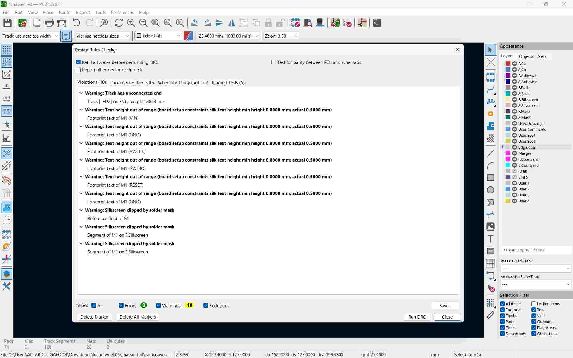
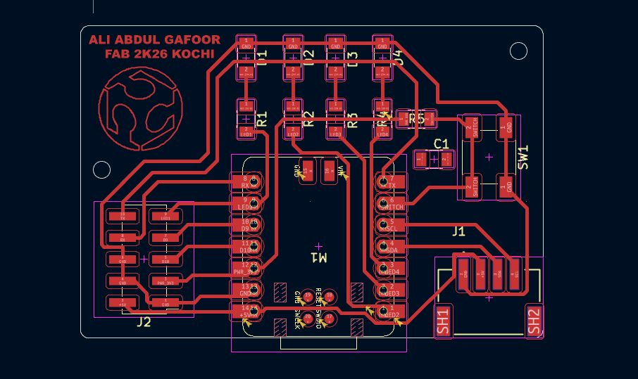
This is how my final PCB looks after designing and routing it in KiCad.
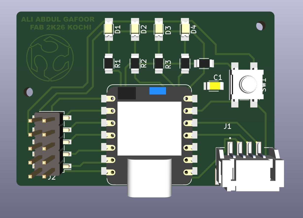
3D PCB Output
This is the 3D view of my PCB generated in KiCad to visualize how the board will look after manufacturing.
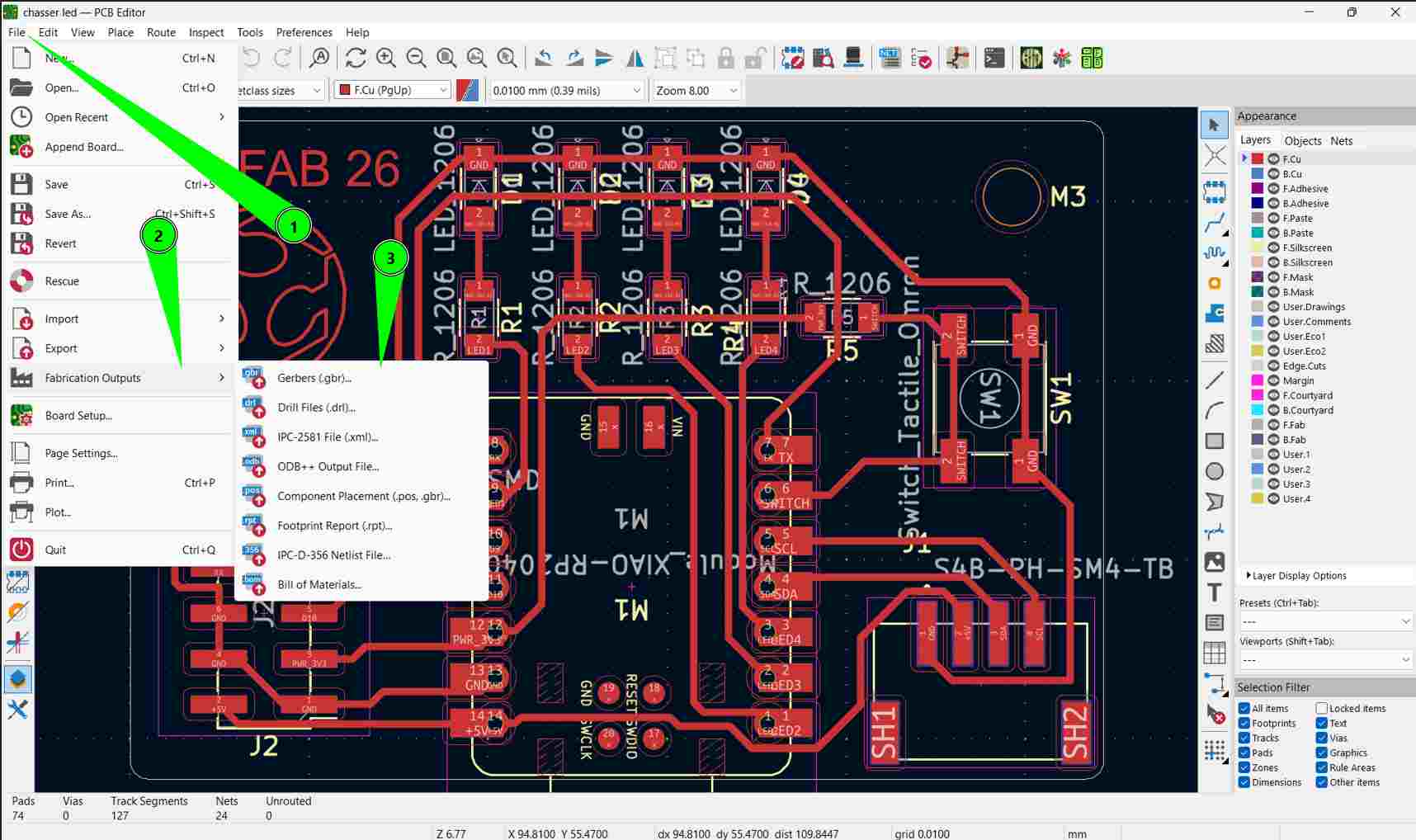
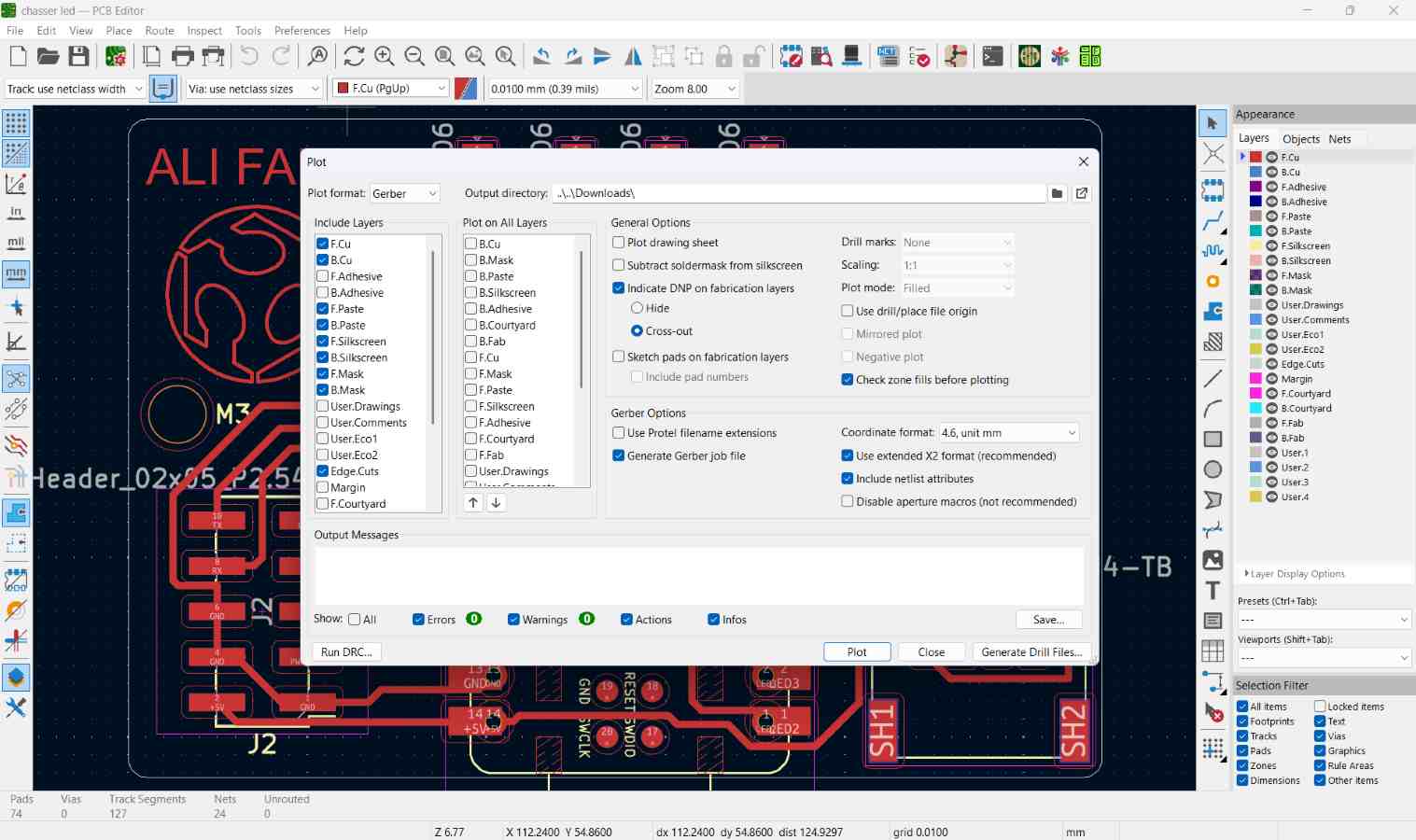
Generating Gerber Files for Fabrication
To prepare the design for manufacturing, we exported the files by navigating to: File → Fabrication Outputs → Gerber Files Gerber files (.gbr) are the standard format used in PCB fabrication. They define all layers of the board, including:
These files act as the blueprint used by PCB milling machines or fabrication services.
choose the output folder and set the required plot options before generating the Gerber files.
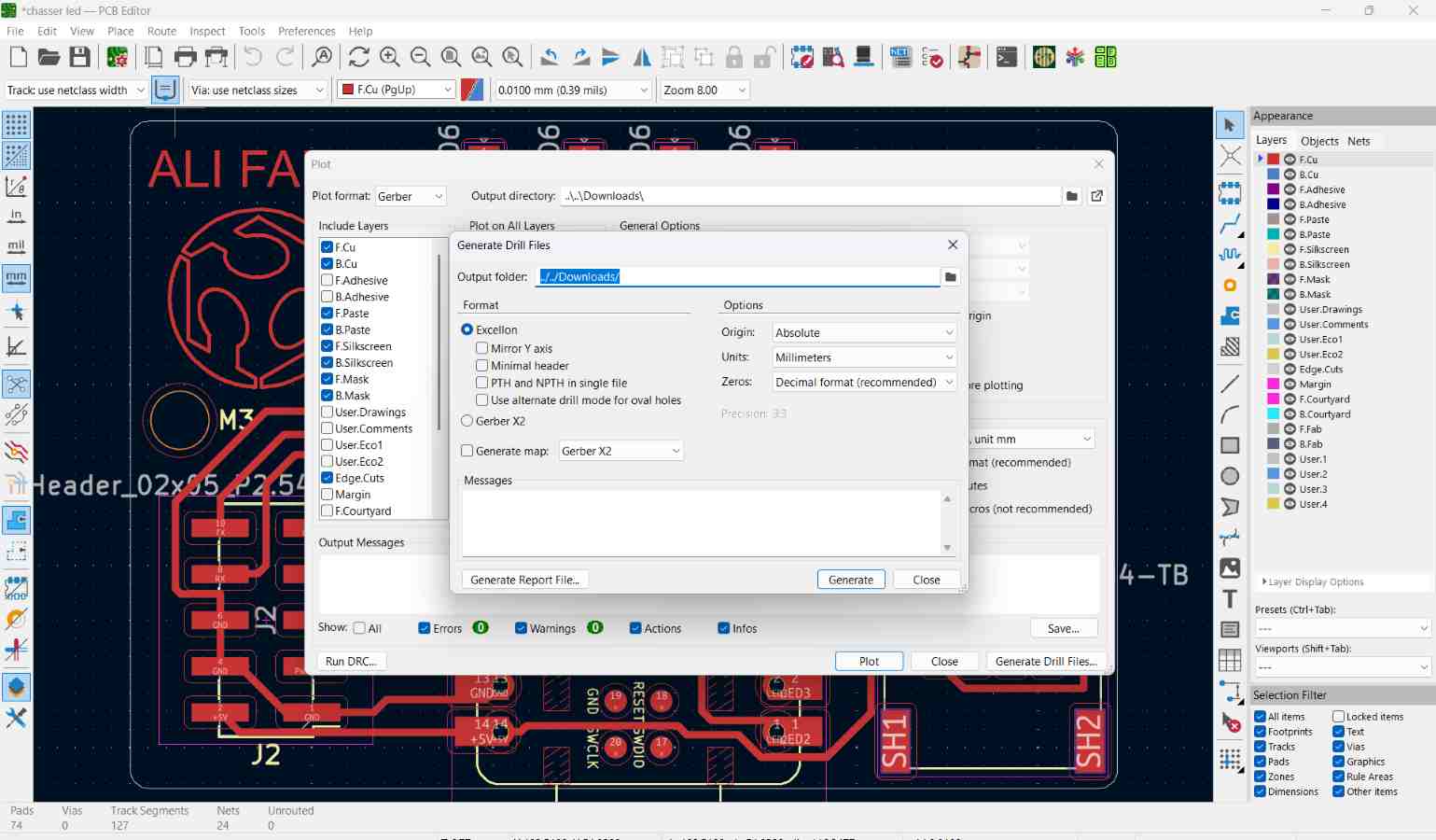
Select the required PCB layers and click Generate Drill Files to export the drill holes along with the Gerber files.
Viewing the Gerber Files
To verify the exported files, we used the online Gerber viewer: pcbway . and gerber2png .This allowed us to visualize each PCB layer and confirm that the traces, pads, and board outline were correct before fabrication.
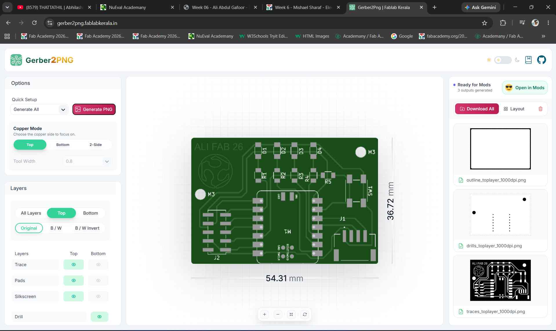
Gerber files viewed using an online Gerber viewer.
Exporting 3D file
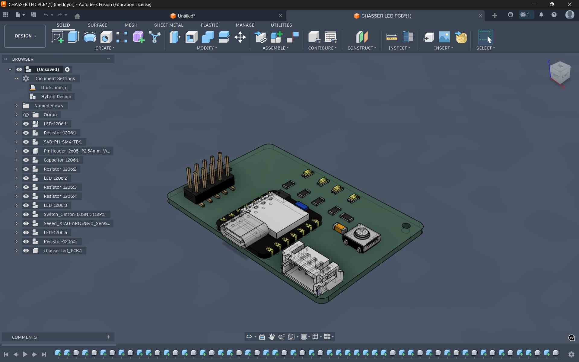
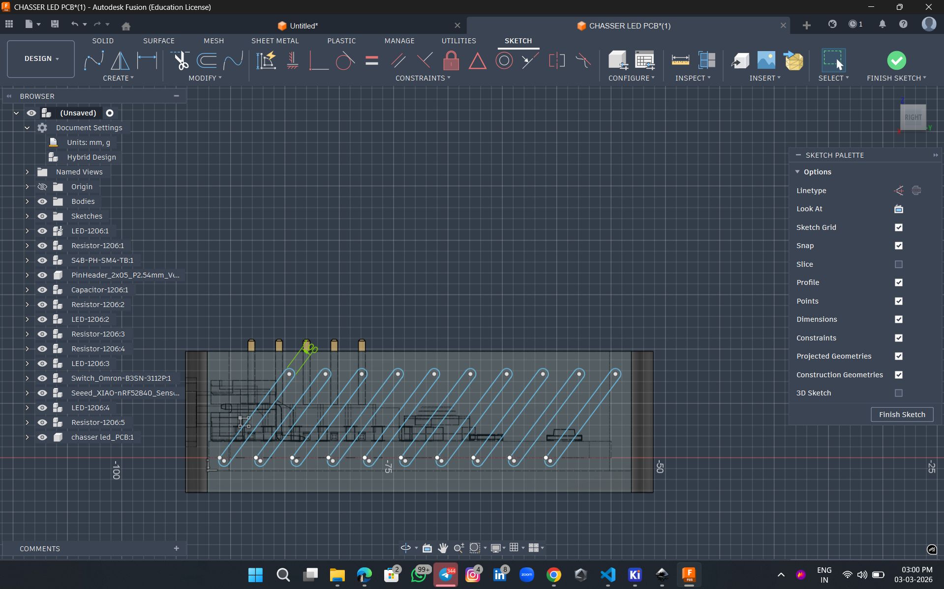
I tried to design a case for the PCB in fusion. I exported the file in pcb editor as step file and opened it in fusion.
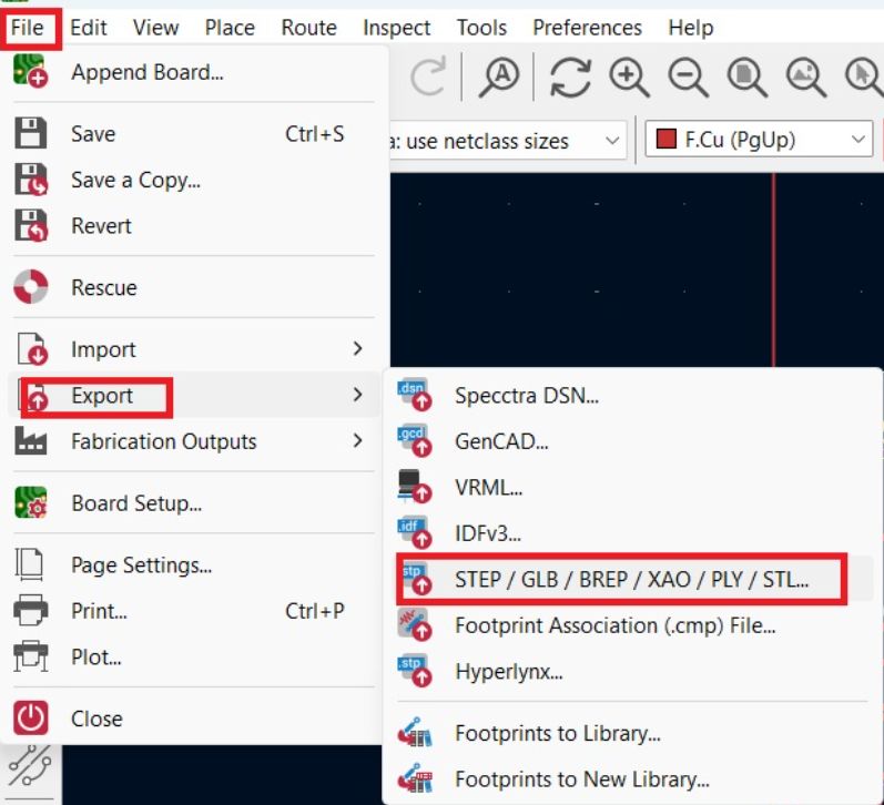
To import file in fusion, open file -> open.
After importing the file, this is how it appears on the screen
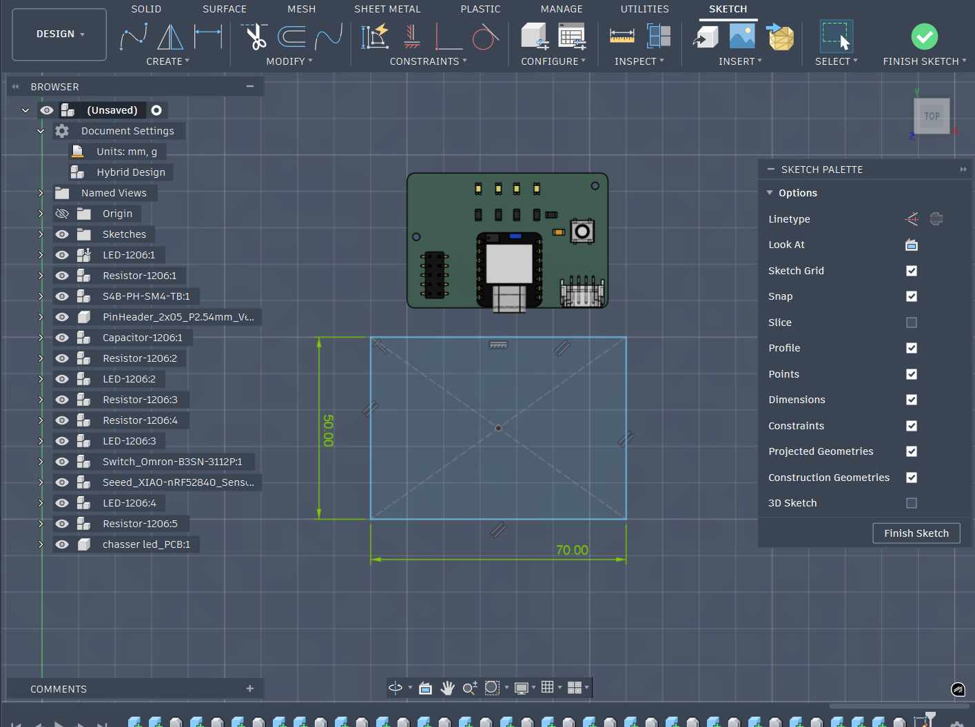
Designing the Enclosure
For the enclosure design, I sketched a 50 mm × 70 mm rectangle and extruded it to 15 mm. After that, I applied the shell operation to achieve a uniform wall thickness of 2 mm.
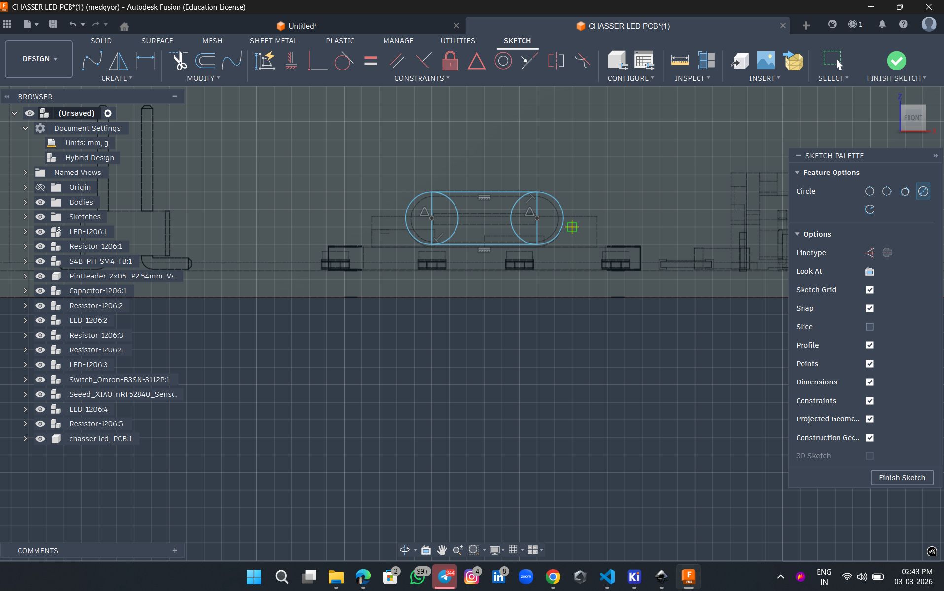
To provide a cable connection, I created a sketch on the top surface of the enclosure and extruded it to form an opening, following the methods learned in Week 02.
Finally, I added a 2 mm fillet to the corners to improve grip and enhance the overall finish of the enclosure.
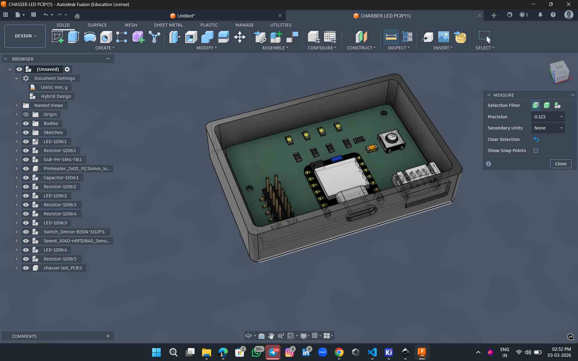
To enhance both the grip and aesthetics, I created a surface texture using a patterned design and extruded it to a height of 0.1 mm.
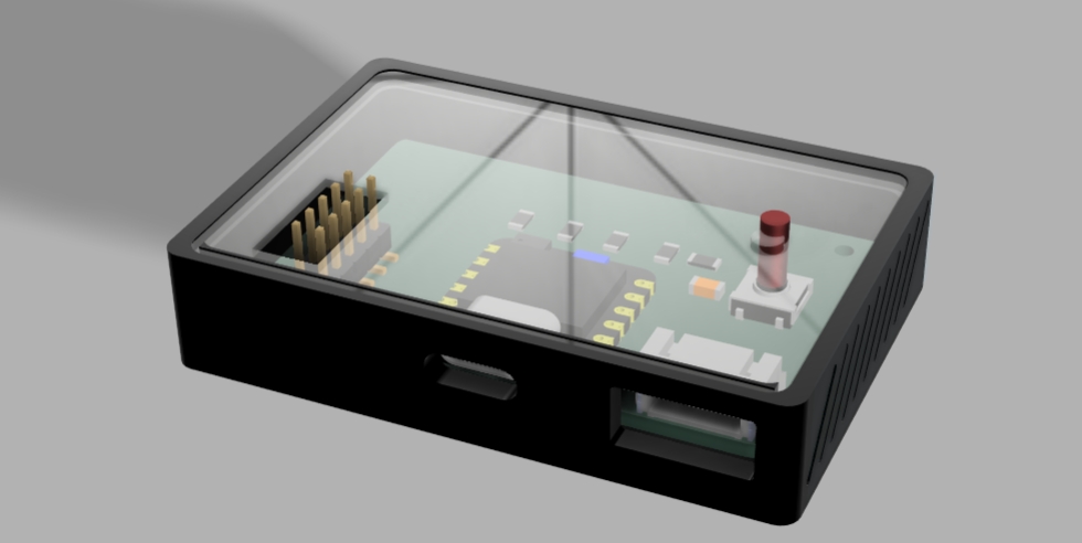
This is the final output after rendering. For the top layer, I am planning to use acrylic, and the remaining body parts will be 3D printed. In the appearance settings, I applied a clear glass material to the top layer to represent acrylic and a standard black finish to the main body
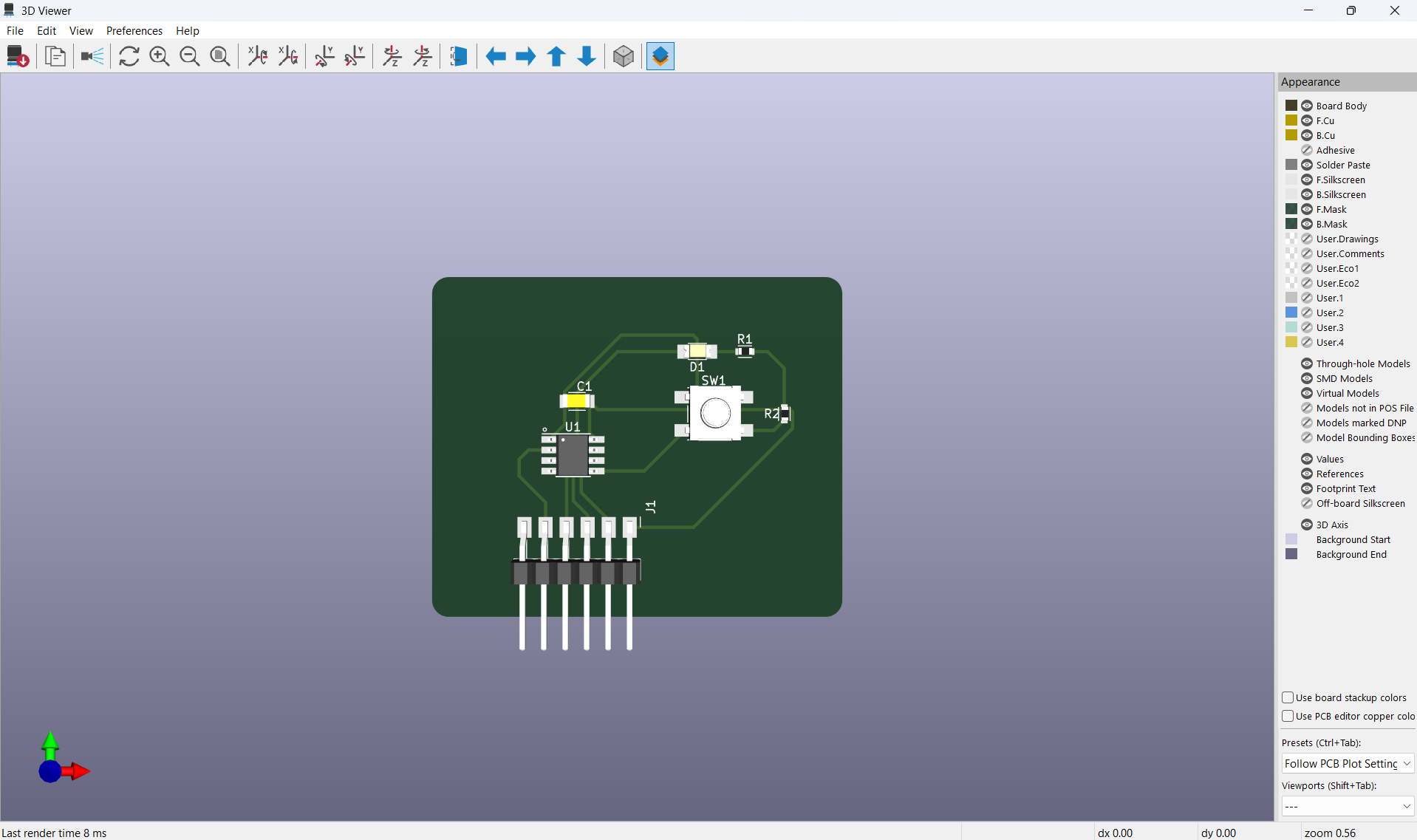
Your Attiny412 PCB
Recreating and Modifying the ATtiny412 Circuit
This was my first experience using KiCad for PCB design. To become familiar with the software, I started by recreating the ATtiny412 development board circuit based on the reference design. After successfully reproducing the original circuit, I made the necessary modifications to suit my project requirements. This exercise helped me understand the KiCad workflow, including schematic creation, component placement, routing, and PCB design, while building confidence for designing more complex boards later in the project.
 Image source .
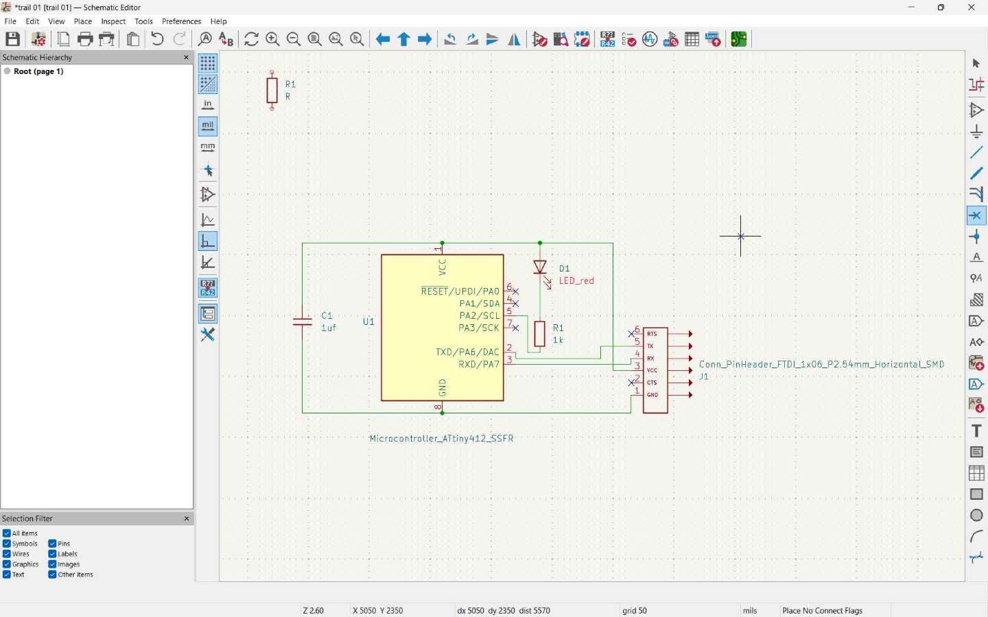
Schematic recreated based on the ATtiny412 reference design.
As a reference, we used Neil's ATtiny412 blink board from the embedded programming week. Following the reference diagram, we recreated the circuit using components from the Fab library. During this process, we:
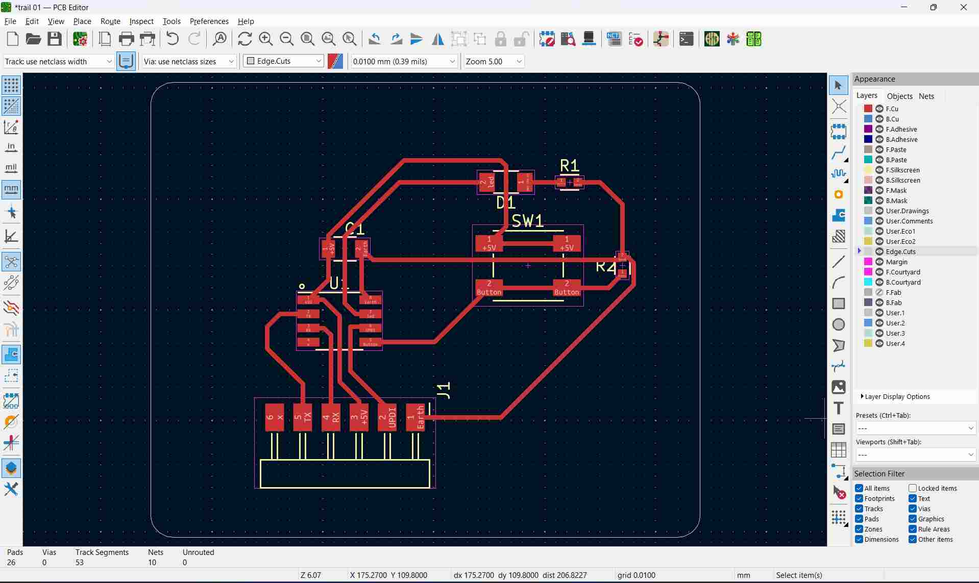
After finishing the PCB layout, I opened the 3D Viewer in KiCad to check the design. It helped me verify the component placement and make sure everything was correctly aligned before fabrication.
Conclusion
In Week 6, I learned PCB design using KiCad, including schematic design and routing. I simulated my circuit in Wokwi before fabrication to test its functionality. After making the PCB, I also designed a protective enclosure for it. This week improved my skills in PCB design, simulation, and integration of electronics with mechanical design.
HERO SHOT:01
HERO SHOT:02