Week 8 – Electronics Production
Introduction To PCB Production
A Printed Circuit Board (PCB) is a flat board made of insulating material with copper pathways etched or milled onto its surface to electrically connect components. Rather than using loose wires to link parts together, a PCB encodes all connections as fixed copper traces, making circuits compact, repeatable, and far easier to assemble.
PCBs are classified by how many copper layers they contain. A single-sided board has copper on one face only — sufficient for simple circuits and the most common format in Fab Lab work. Double-sided boards add copper to the back as well, with drilled holes (vias) connecting the two layers where needed. More complex products use multilayer boards that stack additional copper layers internally, bonded together with insulating sheets.
The base material of a PCB, called the substrate, determines its mechanical and electrical properties. In Fab Labs, FR-1 (a paper-phenolic laminate) is widely used because it machines cleanly and is cheaper than alternatives. FR-4, made from woven glass fiber and epoxy, is the industry standard for commercial boards — it handles heat and moisture better, but is harder on cutting tools. Polyimide (Kapton) is used for flexible boards that must bend in use.
How PCBs Are Made
There are two broad approaches to making a PCB at the desktop level:
Mechanical milling uses a CNC machine fitted with small carbide bits to cut away copper from a copper-clad board, leaving behind the desired traces. The result depends heavily on bit geometry, spindle speed, and how flat and level the board surface is.
Laser ablation uses a focused laser beam to vaporize copper selectively. A fiber-wavelength laser works well on copper, burning away thin copper layers with high precision and no mechanical force on the material.
In both cases, the starting point is a design file — typically created in an EDA (Electronic Design Automation) tool like KiCad — which is exported as a Gerber file or raster image and then converted into machine toolpaths.
The PCB Manufacturing Process
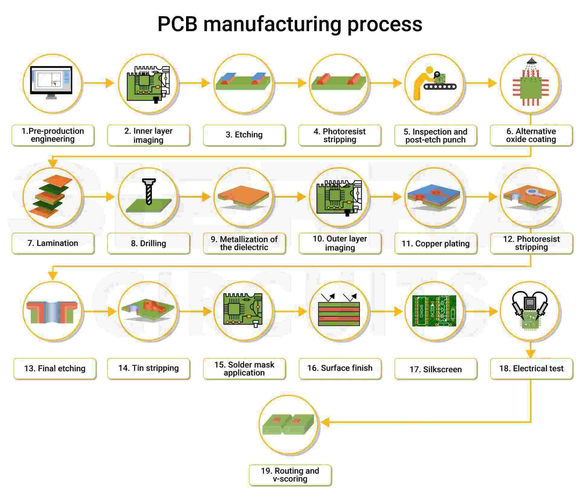
1. Pre-production Engineering Schematic capture and PCB layout are completed in EDA software (KiCad, Altium, Eagle). The design is reviewed for design-rule violations, then exported as Gerber files — the full manufacturing data package covering copper layers, drill locations, solder mask, and silkscreen.
2. Inner Layer Imaging A photosensitive dry film is laminated onto the copper-clad core. UV light is exposed through a photomask derived from the Gerber data, hardening the resist over the areas that will become copper traces. Unexposed resist is developed away.
3. Etching The board is immersed in a chemical etchant (ferric chloride or ammoniacal solution) that dissolves the exposed, unprotected copper, leaving only the trace pattern underneath the hardened resist.
4. Photoresist Stripping The remaining photoresist is chemically stripped away, revealing the clean copper traces on the inner layer.
5. Inspection and Post-Etch Punch Inner layers are inspected by AOI (Automated Optical Inspection) to catch opens, shorts, or dimensional errors. Registration holes are punched for precise alignment during lamination.
6. Alternative Oxide Coating Inner copper surfaces are treated with a chemical oxide (black oxide or brown oxide) to roughen them at a micro scale, improving adhesion to the prepreg bonding sheets in the next step.
7. Lamination Inner layers are stacked in sequence with prepreg (partially cured fiberglass–epoxy sheets) between them. The stack is pressed under heat and pressure in a hydraulic lamination press, fusing everything into a single solid panel.
8. Drilling CNC machines drill through-holes and vias through the laminated panel — hole diameters as small as 0.1 mm for standard vias, with laser drilling used for blind and buried microvias in HDI boards.
9. Metallization of the Dielectric The bare hole walls (fiberglass, not copper) are made conductive using an electroless copper deposition process — a thin seed layer of copper is chemically deposited across all surfaces and inside every hole.
10. Outer Layer Imaging The same photoresist–expose–develop sequence used for inner layers is applied to the outer copper surfaces to define the outer trace pattern.
11. Copper Plating Electrolytic copper plating builds up the copper thickness inside the drilled holes and on the outer traces (typically to 25 µm), ensuring reliable electrical connections through the board.
12. Photoresist Stripping The outer-layer photoresist is chemically stripped, exposing the full copper surface in preparation for final etching.
13. Final Etching A second etch removes the unwanted copper from the outer layers, leaving only the desired trace pattern protected by the plated copper and any remaining etch resist.
14. Tin Stripping Any tin or other temporary etch-resist metal applied over the copper traces is chemically stripped, exposing clean copper ready for surface finishing.
15. Solder Mask Application A liquid photo-imageable epoxy solder mask (most commonly green) is applied across the board, exposed through a mask, and developed. It covers and protects copper traces while leaving component pads exposed, preventing solder bridges during assembly.
16. Surface Finish Exposed copper pads are coated to prevent oxidation and ensure reliable solderability. Common options include HASL (Hot Air Solder Levelling), ENIG (Electroless Nickel Immersion Gold), OSP (Organic Solderability Preservative), immersion tin, and immersion silver.
17. Silkscreen Component reference designators, polarity markers, logos, and assembly notes are ink-jet or screen-printed onto the solder mask, typically in white.
18. Electrical Test Every board is tested for opens and shorts using flying-probe testers or bed-of-nails fixtures. This catches any defects before the boards ship for assembly.
19. Routing and V-Scoring Boards are routed (CNC-profiled) or V-scored to their final outline and separated from the production panel, ready for component assembly.
Types of PCBs
PCBs are categorized by their layer count, flexibility, and substrate material. Each type is optimized for different performance, cost, and form-factor requirements.
Single-Sided PCBs The simplest type — a single substrate layer with components on one side and copper traces on the other. Best suited for low-cost, simple electronics like toys and calculators.
Double-Sided PCBs Conductive metal layers on both sides of the substrate, connected through drilled vias. Allows higher component density and more complex routing, commonly used in automotive dashboards and power supplies.
Multi-Layer PCBs Three or more double-sided boards laminated together with insulating prepreg layers between them. Provides high routing density and signal integrity for advanced applications like servers and medical equipment.
Rigid PCBs Made from a stiff, solid substrate (typically FR-4 fiberglass) that prevents bending or twisting. Offers strong mechanical support and is the standard choice for computers, televisions, and most consumer electronics.
Flexible PCBs (Flex Circuits) Fabricated on flexible polyimide film, allowing the board to bend, twist, and fold. Ideal for compact, lightweight, or high-vibration applications where a rigid board would crack or take up too much space.
Rigid-Flex PCBs A hybrid combining rigid sections (for component mounting and structural support) with flexible sections (for routing between them). Widely used in aerospace, medical devices, and wearables where both strength and space savings matter.
High-Density Interconnect (HDI) PCBs Feature finer trace widths, smaller vias, and higher connection pad density than standard boards. Essential for smartphones, tablets, and high-performance computing where miniaturization is critical.
Metal Core PCBs (MCPCB) Use a metal base layer — usually aluminum — instead of fiberglass to conduct and dissipate heat away from components. The preferred choice for high-power applications such as LED lighting and power electronics.
PCB Substrate Materials
PCB materials are classified primarily by their reinforced base and resin type. The "FR" designation stands for Fire Retardant, and the standards are defined by NEMA (National Electrical Manufacturers Association).
FR-1 (Flame Retardant 1) Made of phenolic resin and paper. Cost-effective for single-sided consumer electronics but highly flammable, with a low glass transition temperature.
FR-2 (Flame Retardant 2) Similar composition to FR-1 (phenolic resin + paper), but with slightly better moisture resistance and higher performance requirements. Commonly found in toys and simple household electronics.
FR-3 (Flame Retardant 3) Composed of epoxy resin on a paper base. Offers better heat and moisture resistance than FR-2, but is still considered inferior to glass-based materials.
FR-4 (Flame Retardant 4) The industry standard. Made from woven fiberglass cloth with an epoxy resin binder. Durable, moisture-resistant, and rated UL 94 V-0. Suitable for single- and multi-layer PCBs across a wide range of applications.
FR-5 (Flame Retardant 5) A higher-performance variant of FR-4 using the same glass fiber and epoxy composition but with a higher glass transition temperature, making it more suitable for demanding thermal environments.
CEM-1 (Composite Epoxy Material 1) A composite grade between FR-2 and FR-4, made with a paper core and glass cloth surfaces. More cost-effective than full glass laminates.
CEM-3 (Composite Epoxy Material 3) Uses a woven glass fabric surface with a paper core, offering higher mechanical strength than CEM-1. Commonly used in consumer electronics.
Metal Core PCBs (MCPCB) Use an aluminum or copper core instead of fiberglass to conduct heat away from components. The standard choice for high-power LEDs and power electronics.
Polyimide (PI) Used for flexible and rigid-flex circuits. Offers high heat resistance and the ability to withstand repeated bending cycles.
Teflon (PTFE) Used for high-frequency, high-speed applications requiring low dielectric loss — such as RF, microwave, and antenna boards.
Comparison Table
| Type | Material Composition | Cost | Key Feature |
|---|---|---|---|
| FR-1 | Paper + Phenolic | Lowest | Very basic, low cost |
| FR-2 | Paper + Phenolic | Low | Common in toys |
| FR-3 | Paper + Epoxy | Moderate | Better than FR-2 |
| FR-4 | Glass Cloth + Epoxy | Moderate | Industry Standard |
| FR-5 | Glass Cloth + Epoxy | High | High thermal resistance |
| CEM-1 | Paper/Glass + Epoxy | Moderate | Cost-effective hybrid |
| PTFE | Teflon | High | High frequency |
PCB Milling Bits
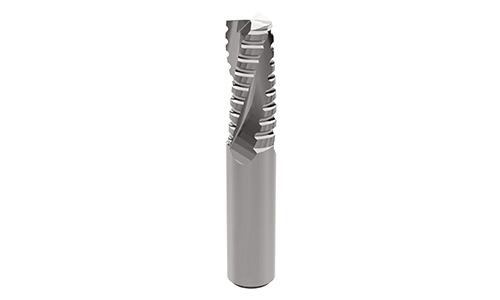
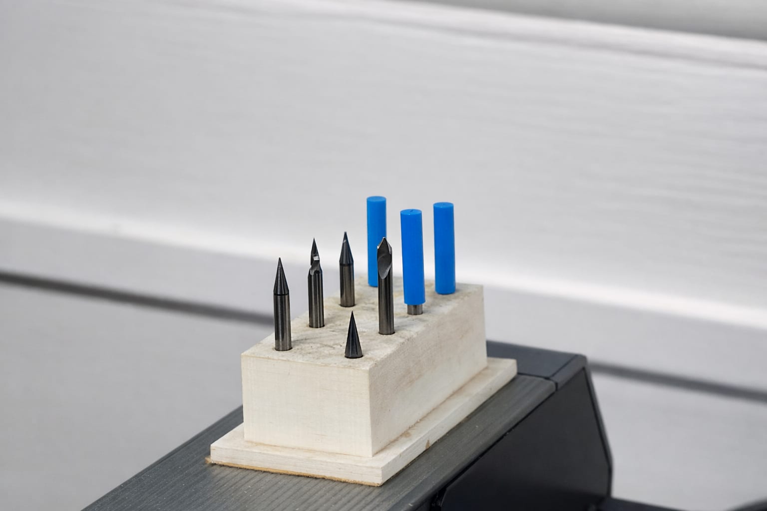
PCB milling bits are specialized solid carbide tools designed for cutting FR-4 and copper at high speeds. Choosing the right bit determines trace quality, minimum feature size, and board edge cleanliness.
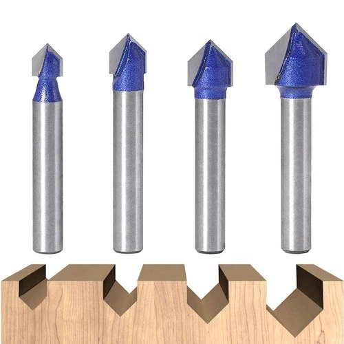
V-Bits (Engraving Bits) The most common bit for isolation milling. The angled tip cuts a V-shaped channel between traces, isolating copper paths without removing large areas of material. 30° and 60° angles are most widely used — a narrower angle produces a finer, more precise cut while a wider angle is more forgiving on uneven surfaces.
Flat End Mills (Two Flute) Used for removing larger areas of copper (pocketing), cutting slots, and routing the PCB outline. Common diameters range from 0.4 mm to 3.175 mm. Two-flute geometry balances cutting efficiency with chip evacuation.

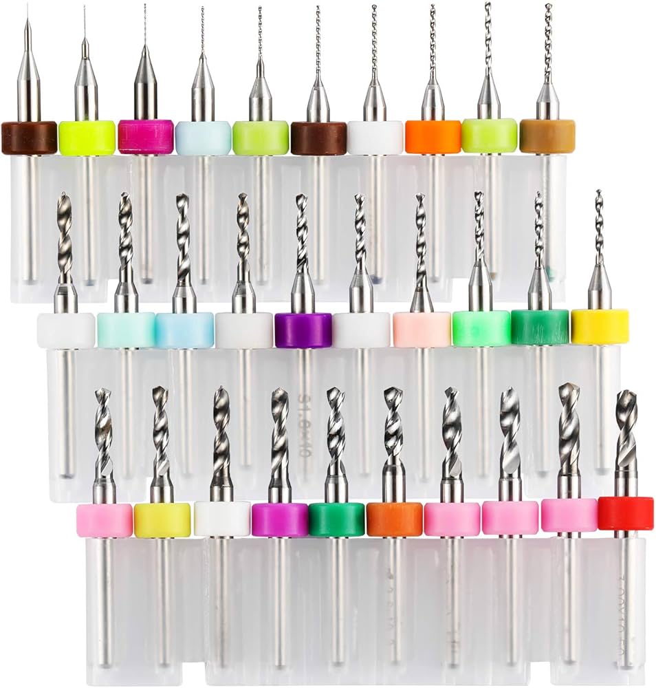
PCB Drill Bits Dedicated tungsten carbide drill bits for creating vias, mounting holes, and through-holes for component leads. Diameters typically range from 0.3 mm to over 3 mm. Smaller vias require precision drill bits run at high spindle speeds.
Chip Breaker Routers Specially designed for routing the PCB outline. The chip-breaker geometry breaks swarf into short segments, preventing clogging and producing clean, smooth board edges with efficient debris removal.
Key Considerations
| Factor | Detail |
|---|---|
| Material | Almost all PCB bits are solid carbide to resist dulling at high speeds |
| Fine-pitch work | 0.1–0.3 mm bits required for tight trace/pad areas |
| General shaping | 0.8–3.175 mm bits used for outline routing and pocketing |
| Cutting direction | Upcut flutes standard for dust evacuation; downcut used to prevent surface splintering |
What This Week Covers
At Super Fablab Kochi, the group tested three fabrication approaches side by side: CNC milling on the Roland MDX-20, copper engraving on the xTool F1 Ultra fiber laser, and ordering boards through a commercial board house. Each method was evaluated for the finest trace width and clearance it could reliably produce, the preparation required, and the overall quality of the finished board.
Roland MDX-20 PCB Milling Workflow - Mishael, Ali, Ardra
Machine Overview
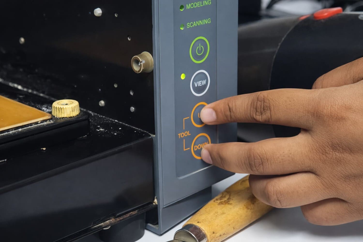
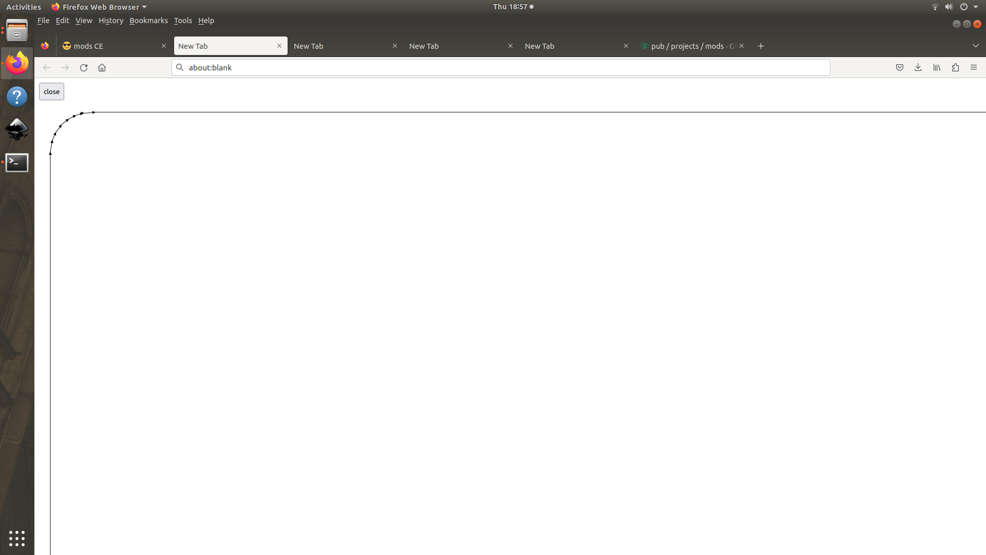
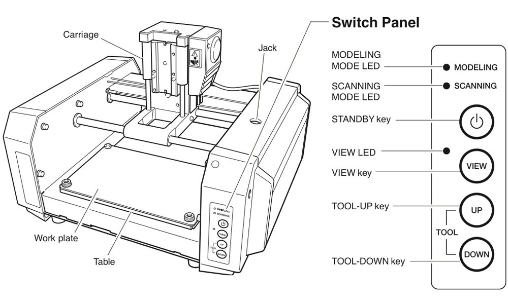 View key.
The View key acts a pause button. When pressed, it brings the work plate out as shown in the image. We can observe the cut depth. Press the button again to continue the milling process.
The Roland Modela MDX-20 is a compact 3-axis (X, Y, Z) desktop milling machine used for precision fabrication tasks such as PCB prototyping. It is widely used in educational and small-scale production environments due to its reliability and fine control over toolpaths.
Incase of an Emergency or if there are changes to be made.
Press View key this pauses teh machine and moves the plate towards the user.
Select “Close socket” in the mods software.
The “up” and “down” buttons are pressed together to reset the machine. The “View LED” blinks for few seconds and stops.
Press View key on the machine and then select “Open Port” in the mods software. After this select “Move to origin” continue the steps to mill
Incase of an Emergency or if there are changes to be made.
Press View key. his stops the spindle and moves the plate towards the user.
Select Close so
The up and down buttons are pressed together to reset the machine. The
Required Tools and Materials
Before starting, ensure the following are available:
- Copper-clad board
- Thin double-sided tape (for mounting)
- End mills / V-bits:
- 0.2 mm, 60° V-bit (standard traces)
- 0.4 mm flat end mill
- 0.8 mm flat end mill (outline cutting)
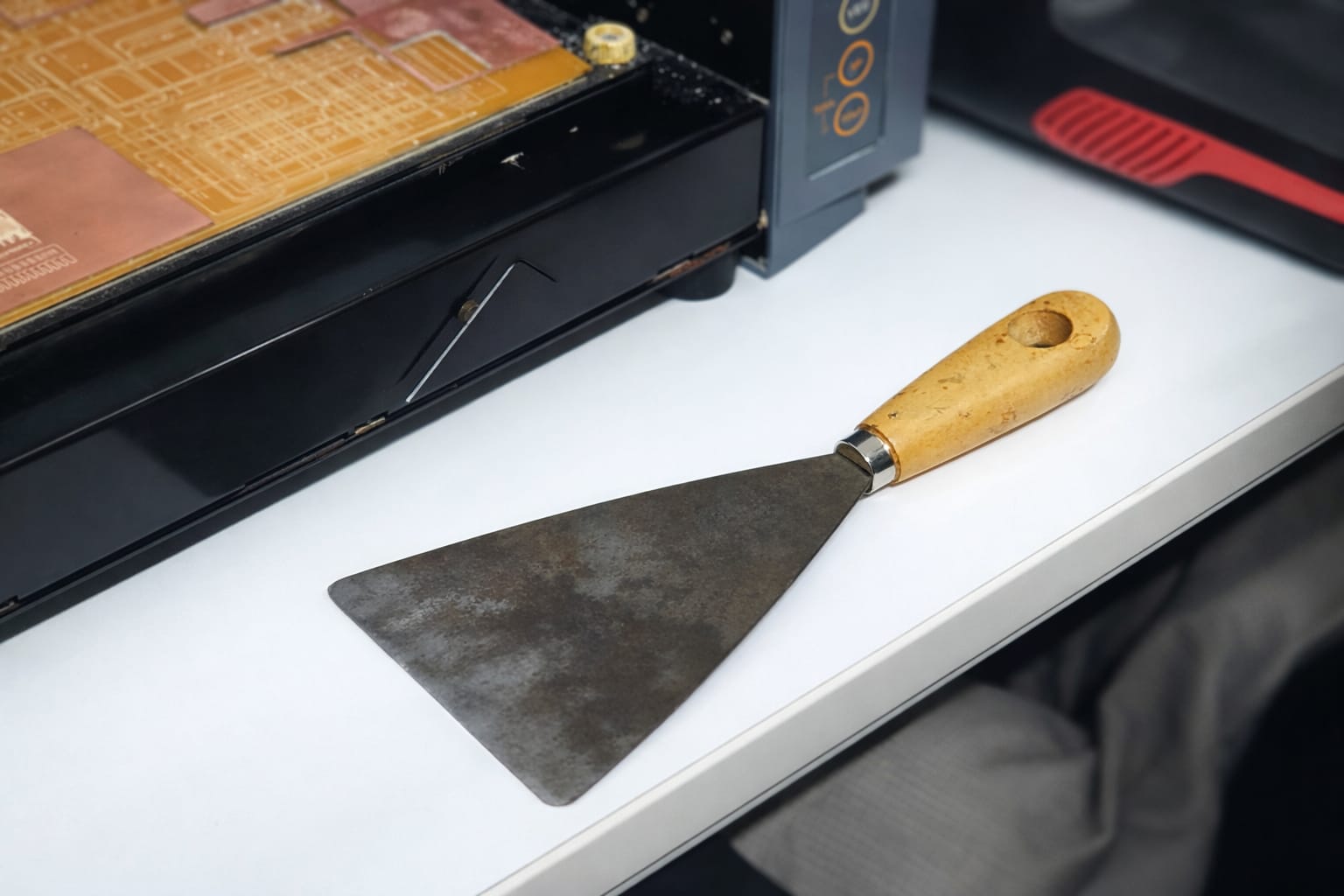
- Scraper (board removal)
- Allen key (tool tightening)
- Vacuum cleaner (chip removal)
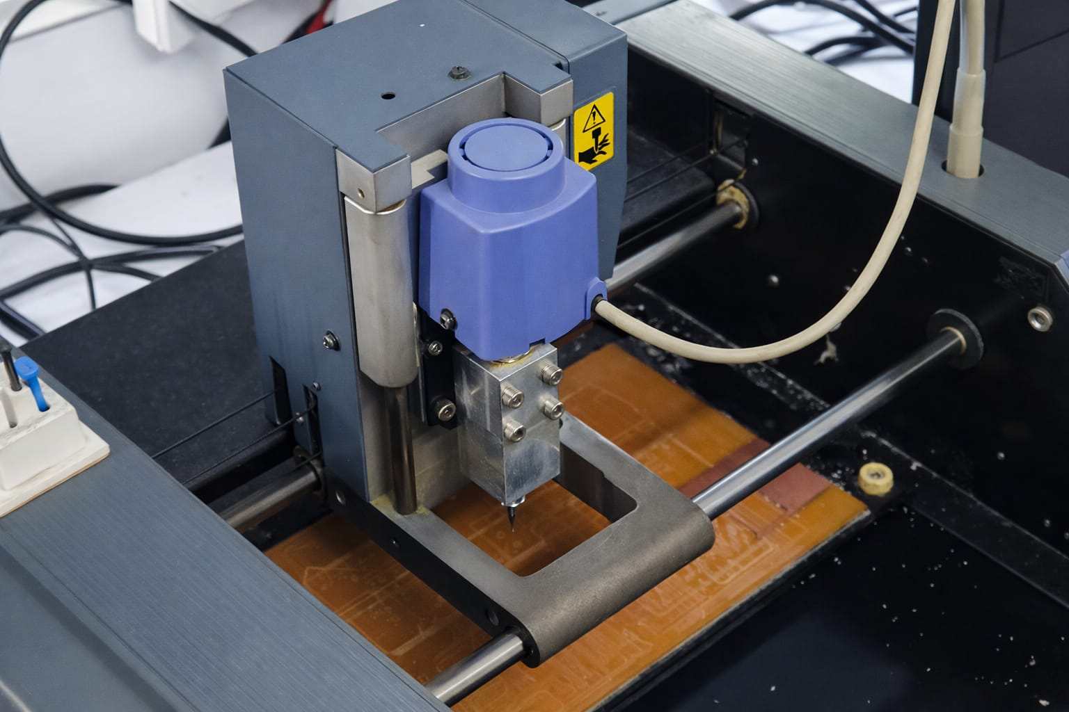
Machine Setup
(image of the machine)
- Power On
- Turn on the machine using the power button.
- The machine will automatically move to its home position.
- Mount the PCB
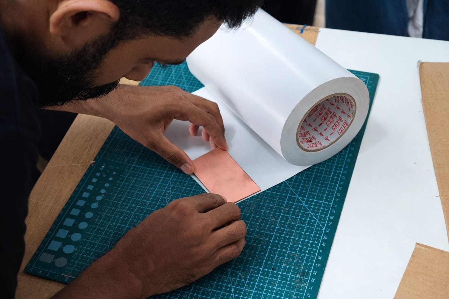
- Apply double-sided tape evenly on the back of the copper board.
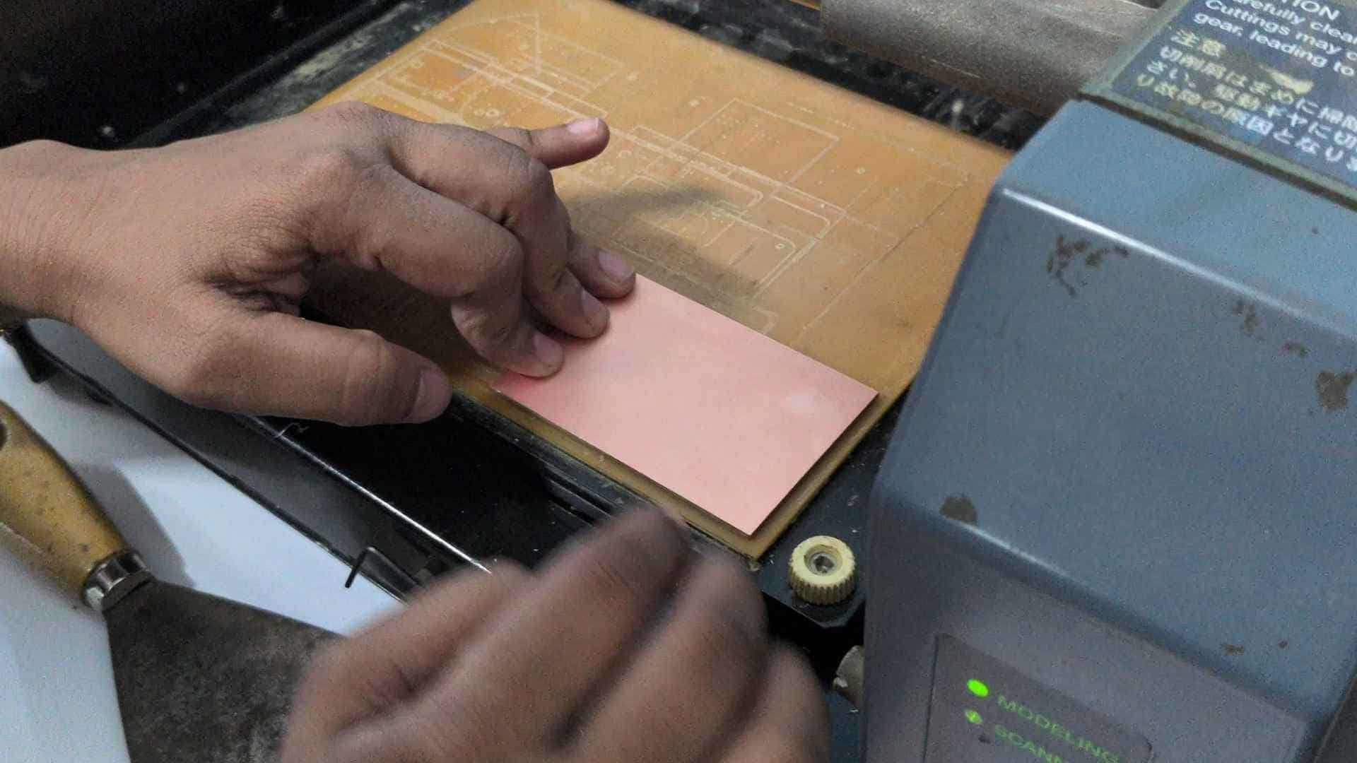
- Fix the board firmly onto the machine bed.
- Ensure there are no air gaps, as uneven surfaces affect milling depth.
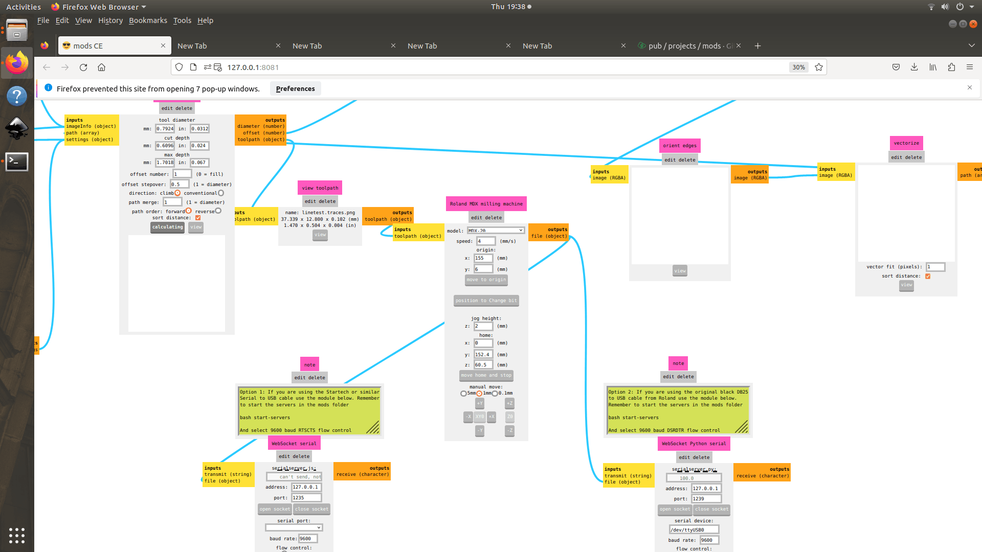
- Open Mods Workflow
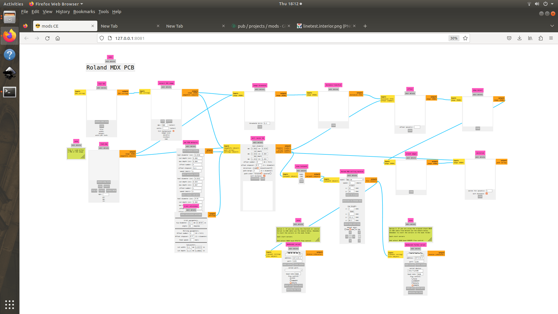
Launch Mods (browser-based interface).
Select:
Programs → Open Program → Roland MDX → PCB
This loads the PCB milling workflow with modules for:
- PNG input
- Toolpath generation
- Machine communication
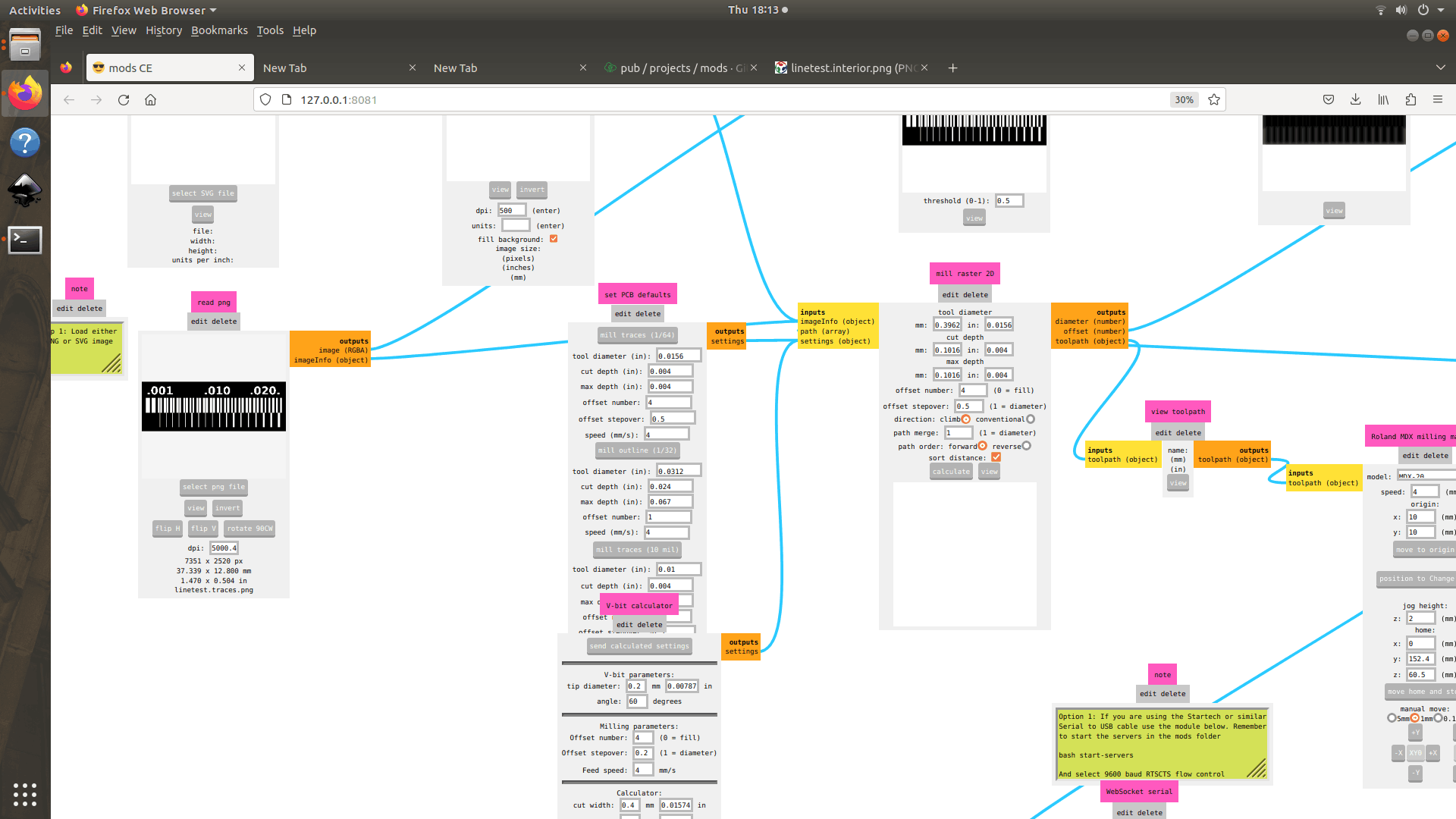
Milling Traces
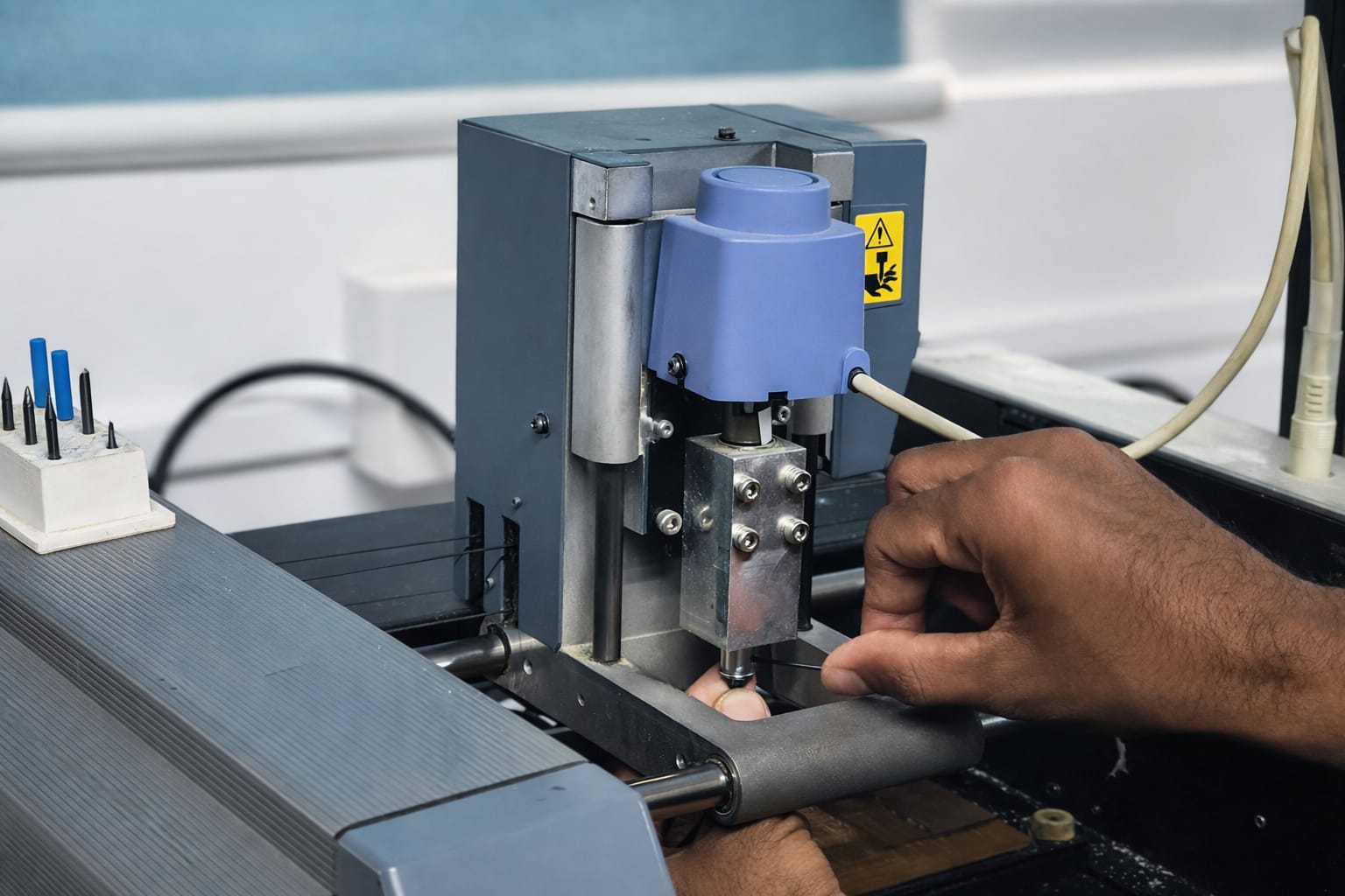
- Tool Selection and Installation

- Choose a suitable bit (commonly 0.2 mm, 60° V-bit).
- In Mods, click “Move to change position”.
- Insert the tool as deep as possible into the collet, the flute should be still visible outside the collet.
- Tighten securely using the Allen key.
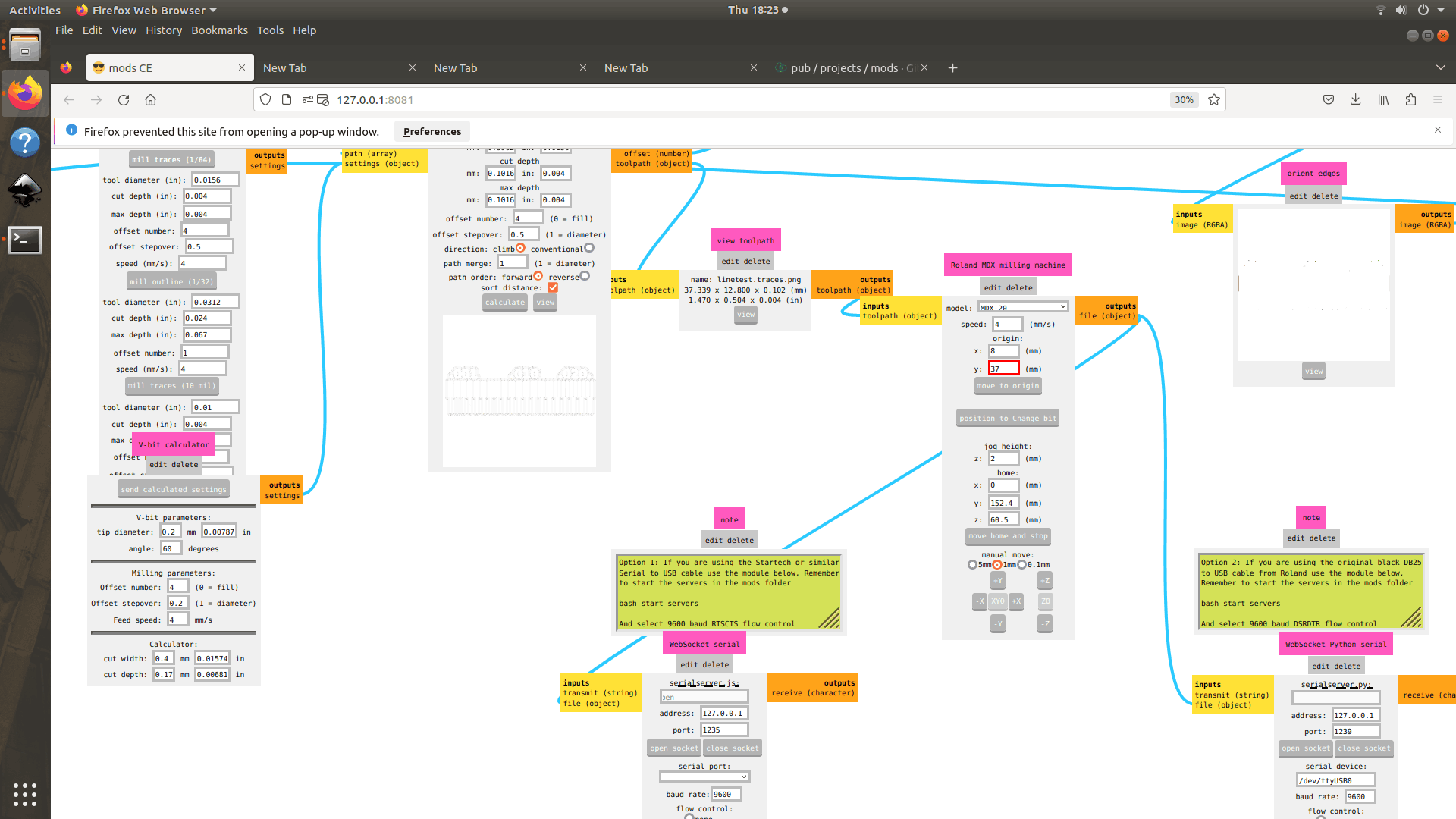
- Set Origin (X, Y)
- Take approximate measurements of the desired origin by measuring the bed after positioning the copper clad board.
- Enter the (x, y) mm values in the Mod, change till satisfied with the bit’s position.
- This location becomes the (0,0) origin. (Note the values)
- Ensure the origin is within the copper surface boundary.
- Set Z Offset (Critical Step)
- Lower the tool close to the PCB surface using step controls.
- Loosen the tool slightly.
- Let the bit gently touch the surface.
- Retighten the tool.
This ensures accurate cut depth, which is essential for isolating traces without overcutting.
- Load and Configure File
- Import the trace PNG file into Mods.
- If using a V-bit:
- Use the V-bit calculator.
- Input parameters (cut depth = .09mm).
- Send calculated values to mill raster 2D.
- Click “Calculate” to generate the toolpath.
- Send Job and Mill
- Verify the generated toolpath.
- Click Send File in WebSocket Python serial box.
- The machine starts milling.
- Use a vacuum cleaner while pausing the operation to remove debris.
Milling Outline
- Change Tool
- Replace the tool with a 0.8 mm end mill.
- Repeat Z offset calibration.
- Keep the same X, Y origin.
- Generate Outline Toolpath
- Load the outline PNG file.
- Select “Mill outline” in Mods.
- Set appropriate parameters (cut depth, passes).
- Click “Calculate”.
- Cut and Remove Board
- Send the file to the machine.
- After cutting, carefully remove the board using a scraper.
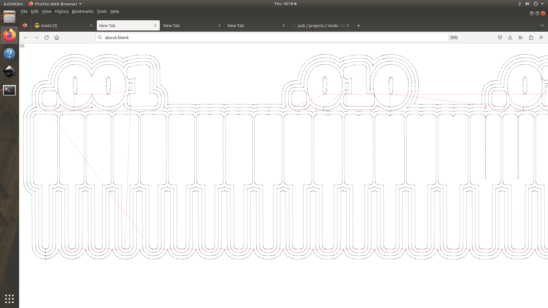
Final Output
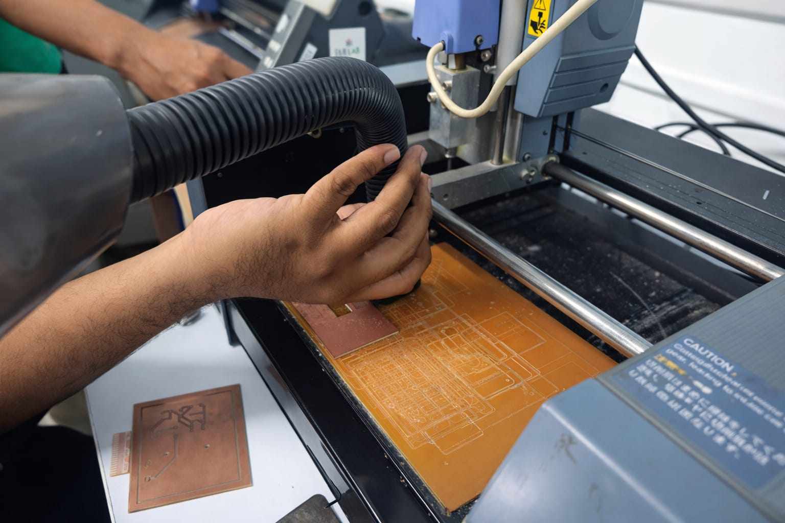
The first test piece was traced using a 0.4 mm flat end mill, while the one on the right was done using a 0.2 mm V-bit. For the individual assignment, a V-bit is being used.
- Inspect traces for continuity and isolation.
- Clean excess copper dust if required.
Observations and Constraints
- Minimum trace width: 0.3 mm (v-bit)
- Minimum trace spacing: 0.4 mm
- Smaller spacing increases risk of:
- Trace bridging
- Incomplete isolation
These values depend on:
- Tool geometry
- Machine calibration
- Surface flatness
Notes for Improvement
- Surface leveling significantly affects results; uneven boards lead to inconsistent trace depth.
- Always verify tool paths before milling to avoid material waste.
PCB Engraving using XTools F1 Ultra - Ashtami , Archita
Task overview:
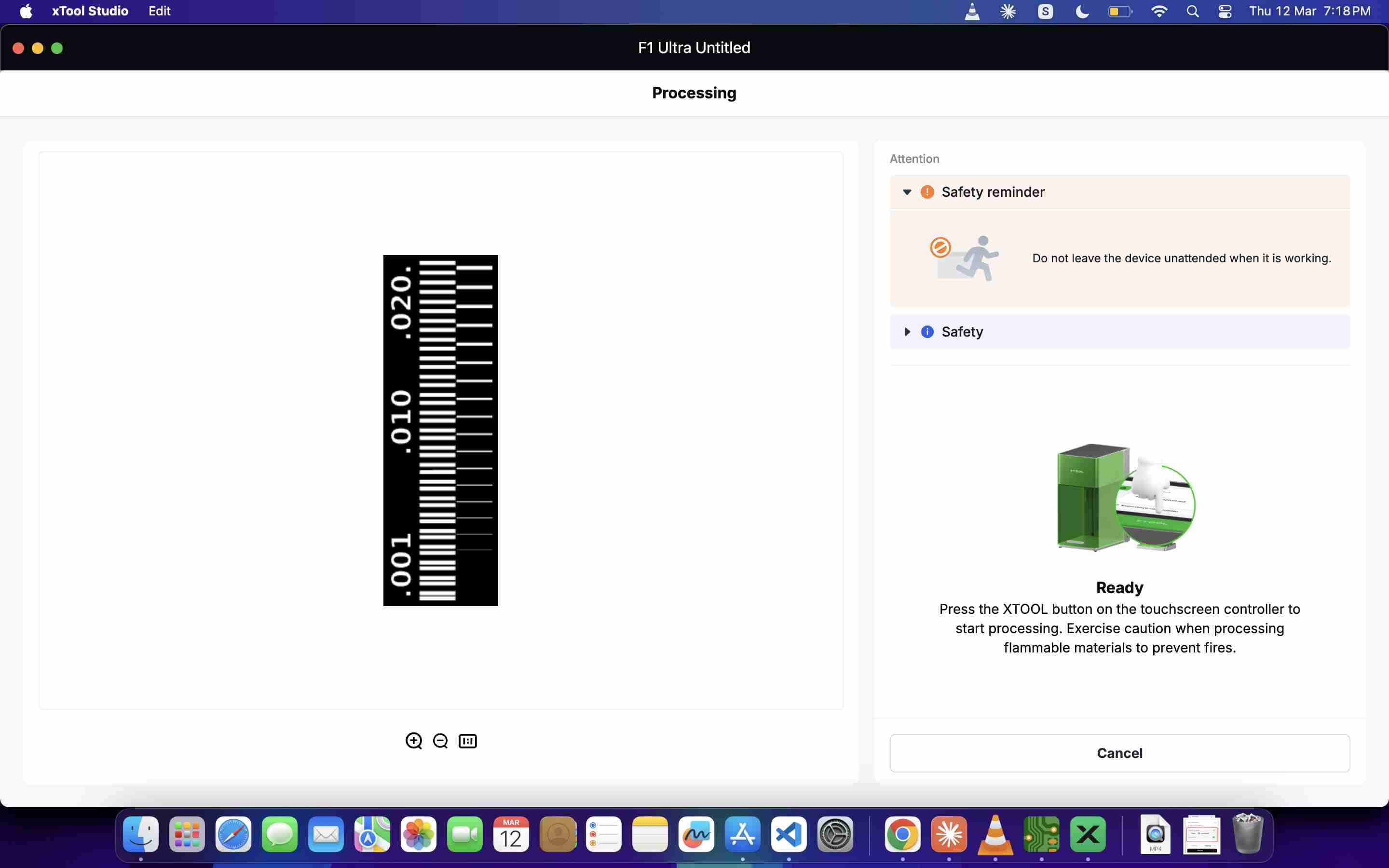
For testing different workflows to fabricate PCB boards, we used the xTool F1 Ultra laser engraver. Comparing with PCB milling process, this method felt much faster because we don’t need to change milling bits or create multiple toolpaths. The laser removes the unwanted copper from the board to form the circuit traces.
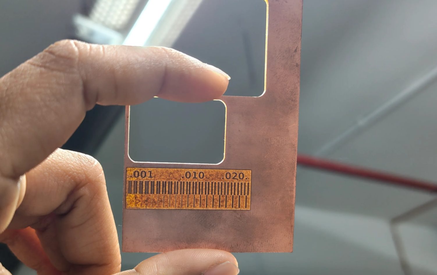
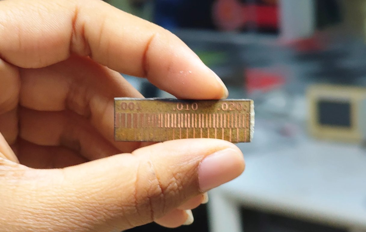
To evaluate how precise this process is, we used the Fab Academy line test pattern (exterior and interior). This pattern contains traces with different widths and spacing. It helps us find the minimum trace width and clearance that our workflow can produce. During engraving, the laser removes the copper between the lines, leaving the copper tracks that form the circuit. By observing which traces remain clear and which ones merge together, we can understand the fabrication limits of this laser-based PCB workflow.
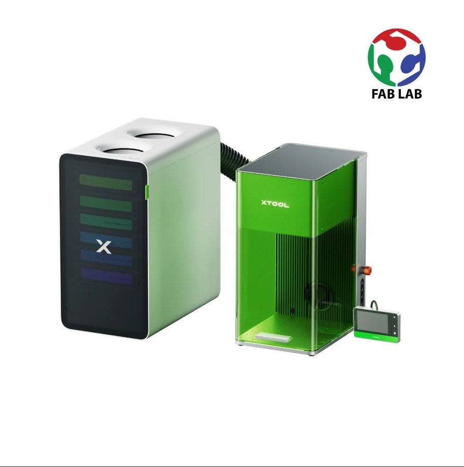
Machine used:
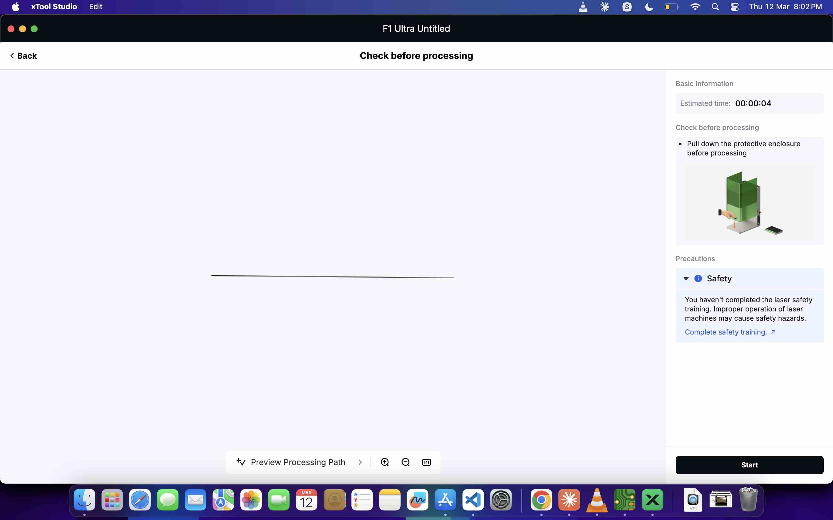
The xTool F1 Ultra is a compact desktop laser machine used for engraving, marking, and cutting.
It has two lasers:
Fiber IR laser: Used for engraving and marking metals like copper, steel, and aluminum.
Blue diode laser: Used for cutting and engraving non-metal materials like wood, acrylic, leather, paper, and fabric.
It is commonly used for rapid prototyping and small fabrication tasks.
Workflow – PCB engraving using xTool F1 Ultra
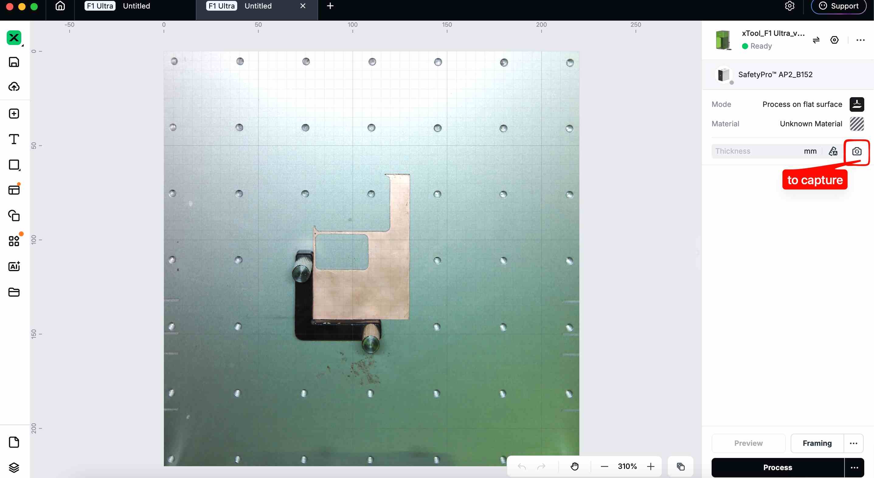
First, we placed the copper clad board on the bed of the xTool F1 Ultra. Then we opened xTool Creative Space and connected the machine to the software.
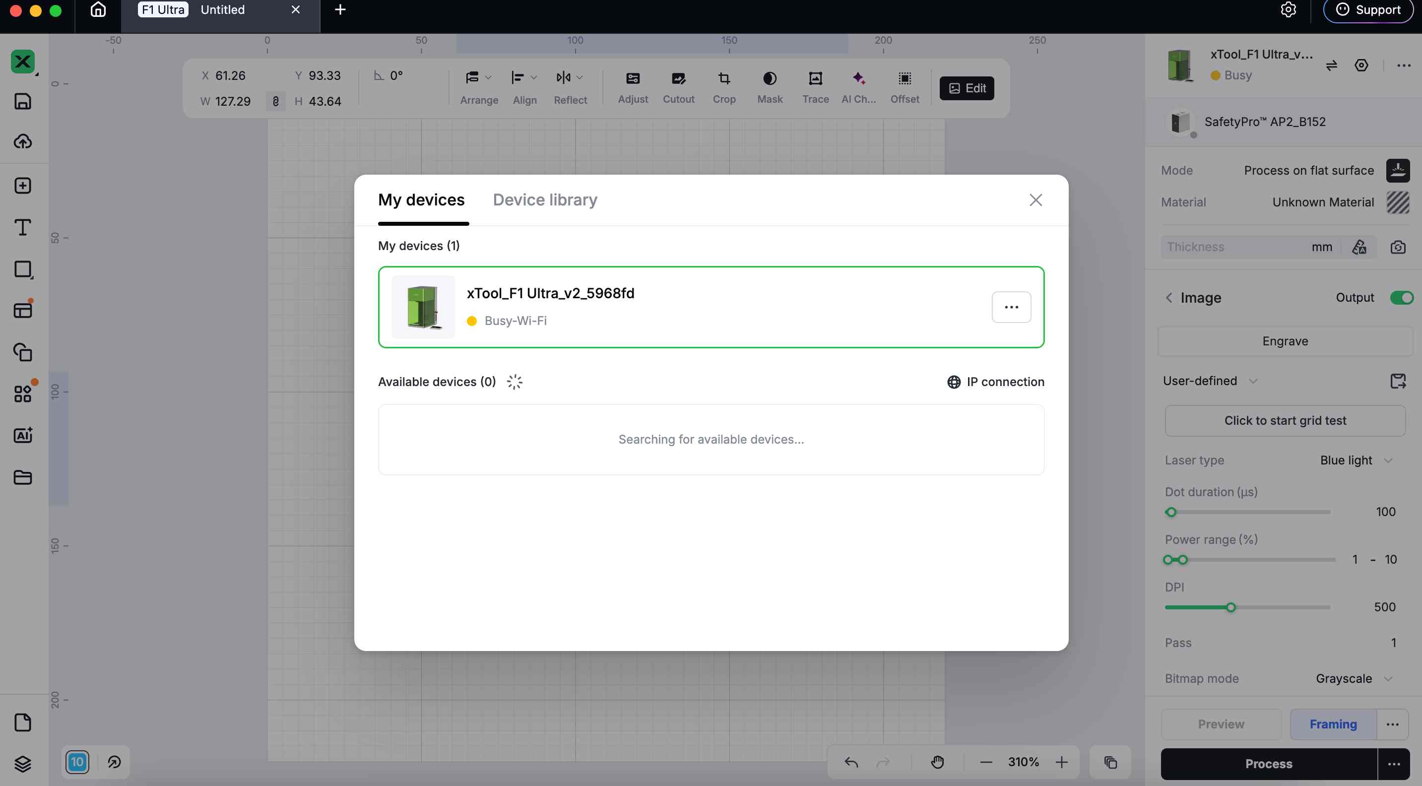
Using the camera feature in the software, we captured the position of the copper clad board so the design could be framed (aligned) correctly.
After that, we imported the linetest.traces_exterior.png
Once the PNG was selected, the Trace option appeared in the top toolbar.
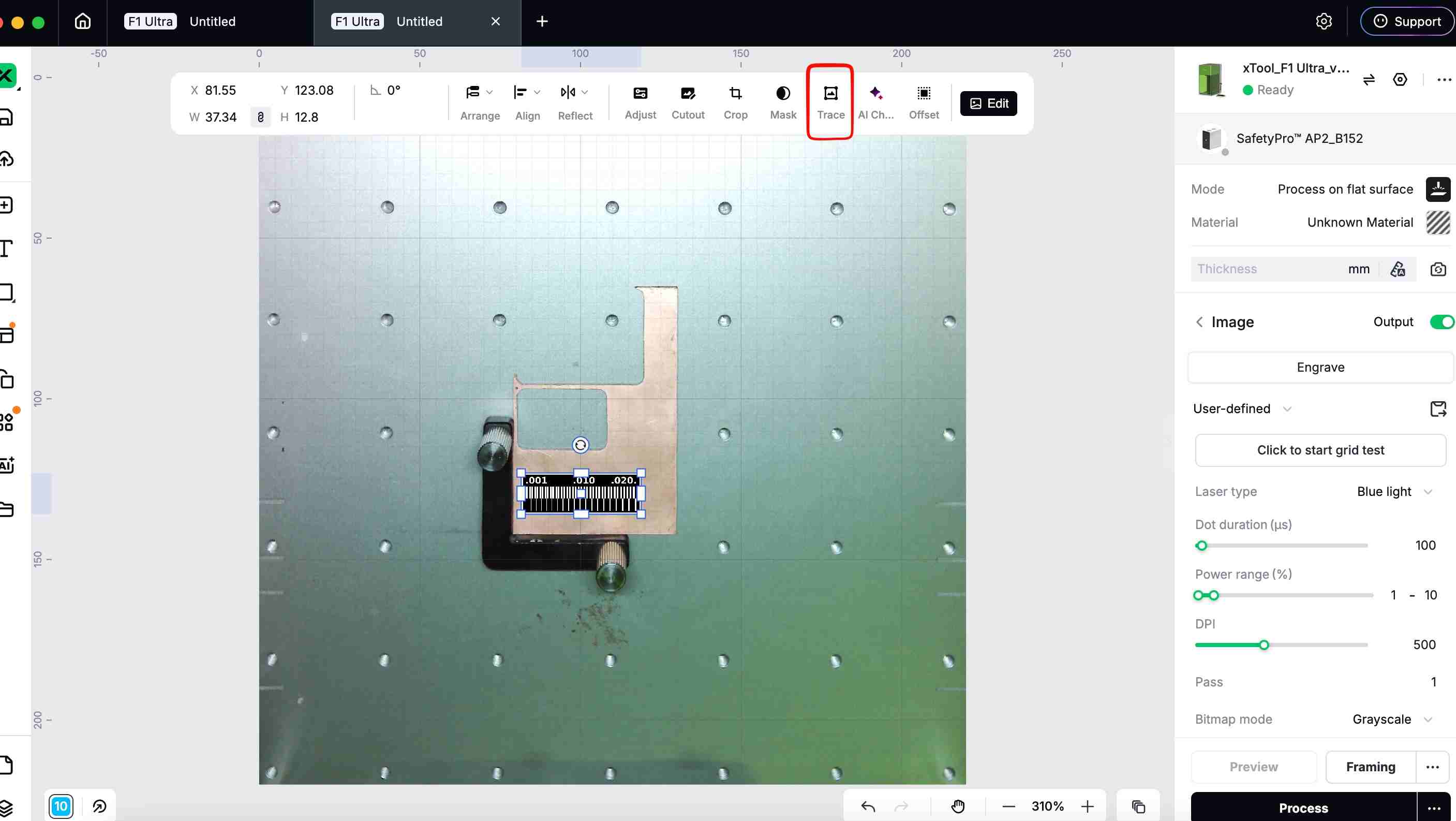
Using trace, we converted the PNG into a vector path.
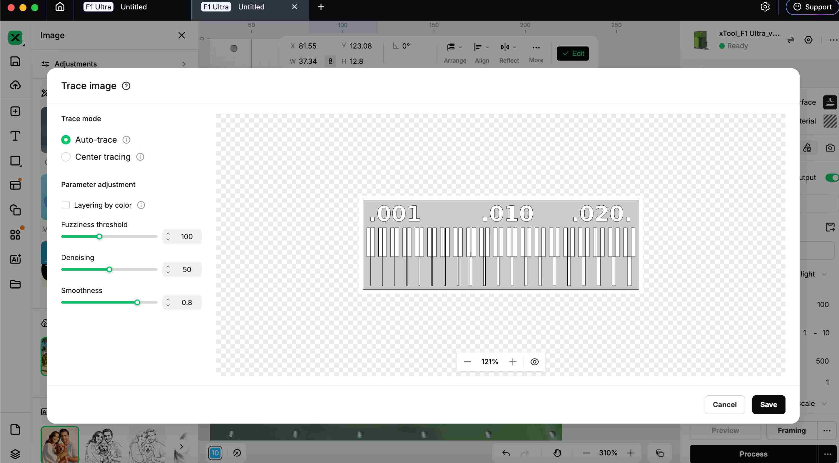
After tracing, both the original PNG and the traced vector overlapped. So in the Layers panel, either hid or deleted the PNG, keeping only the vector.
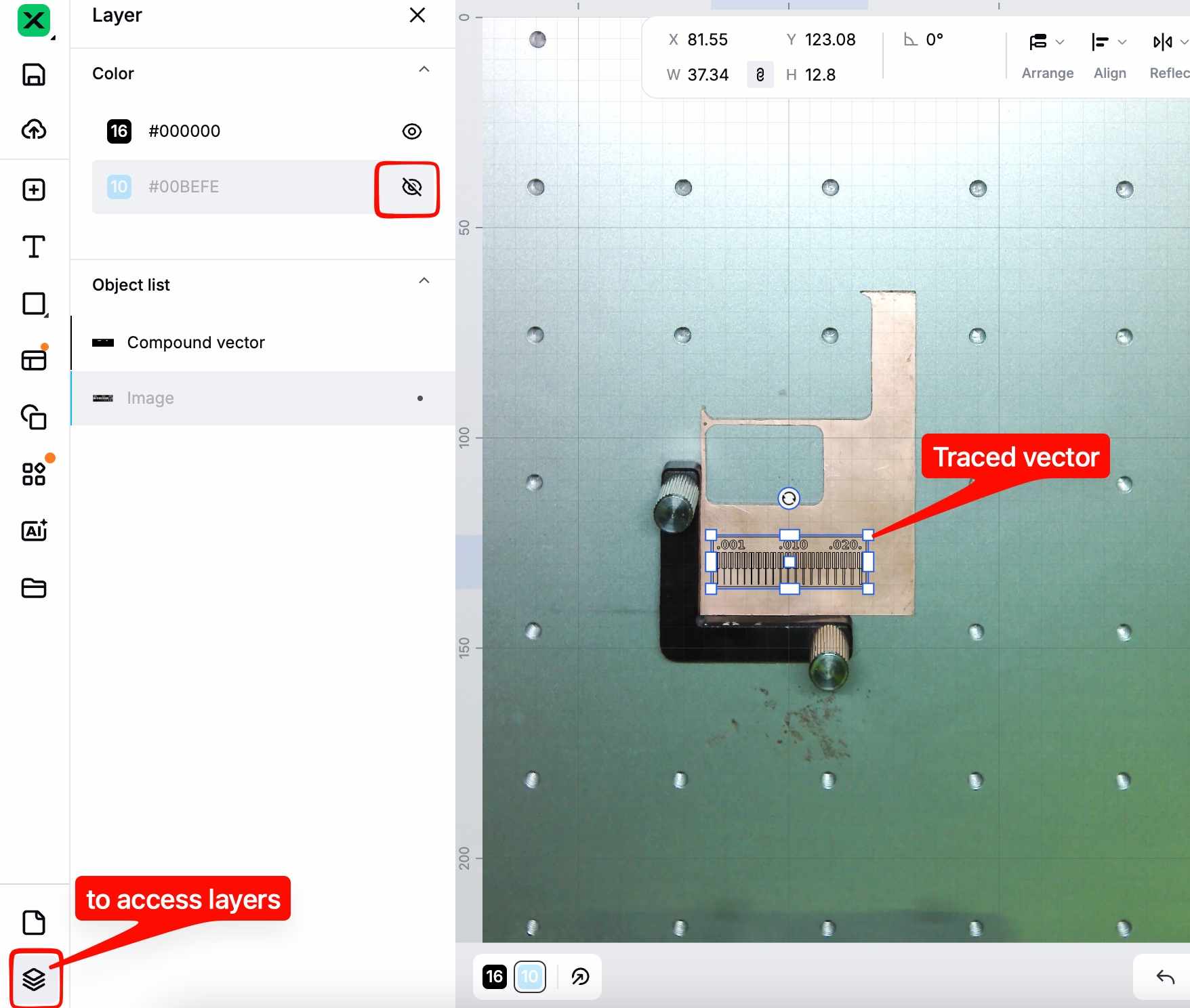
Next, we selected the traced vector. On the right panel, the software shows three options:
- Score
- Engrave
- Cut
For this process, we selected Engrave.
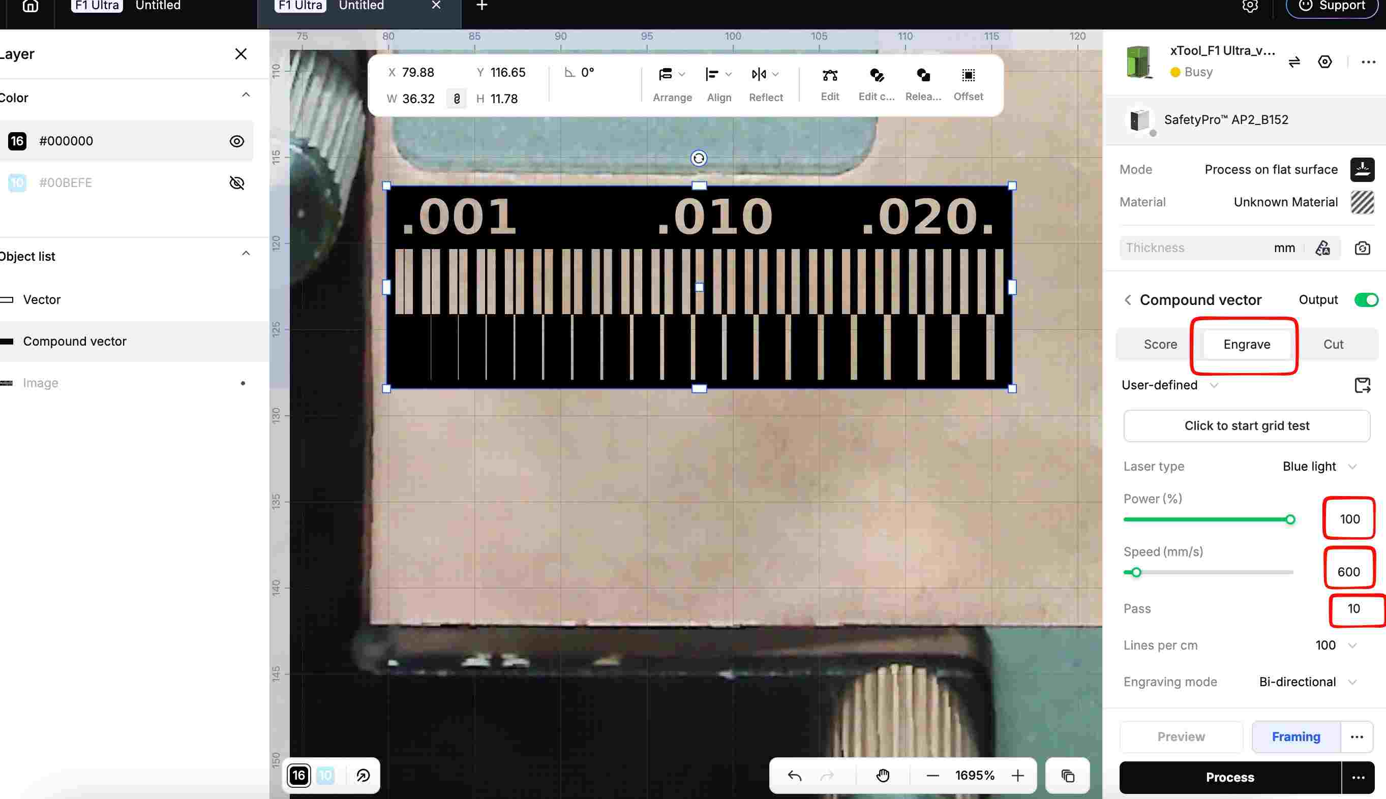
Since we were using a custom material, we manually set the parameters:
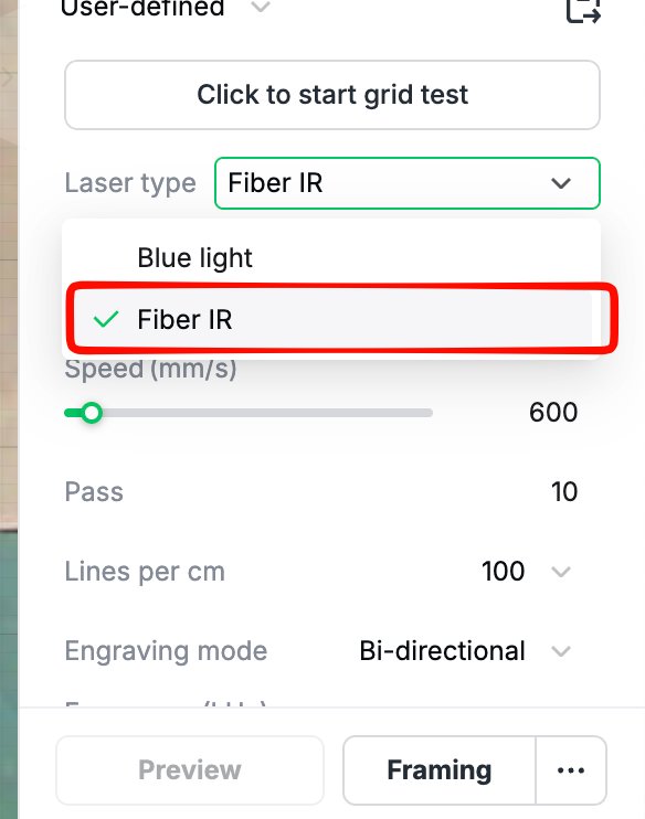
- Laser type: Fiber IR
- Power: 100%
- Speed: 600
- Passes: 10
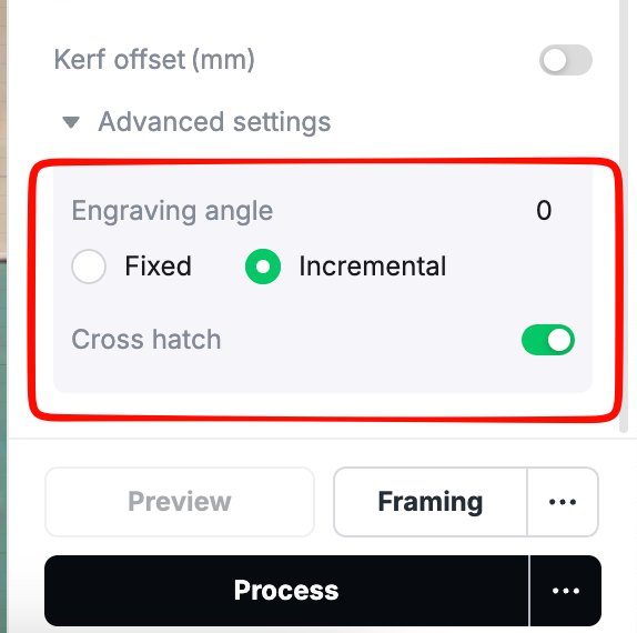
In the Advanced settings, we set:
- Engraving angle: Incremental (The engraving direction changes slightly with each pass for more even material removal.)
- Mode: Cross hatch (The laser engraves in two directions (horizontal and vertical) to remove copper more evenly.)
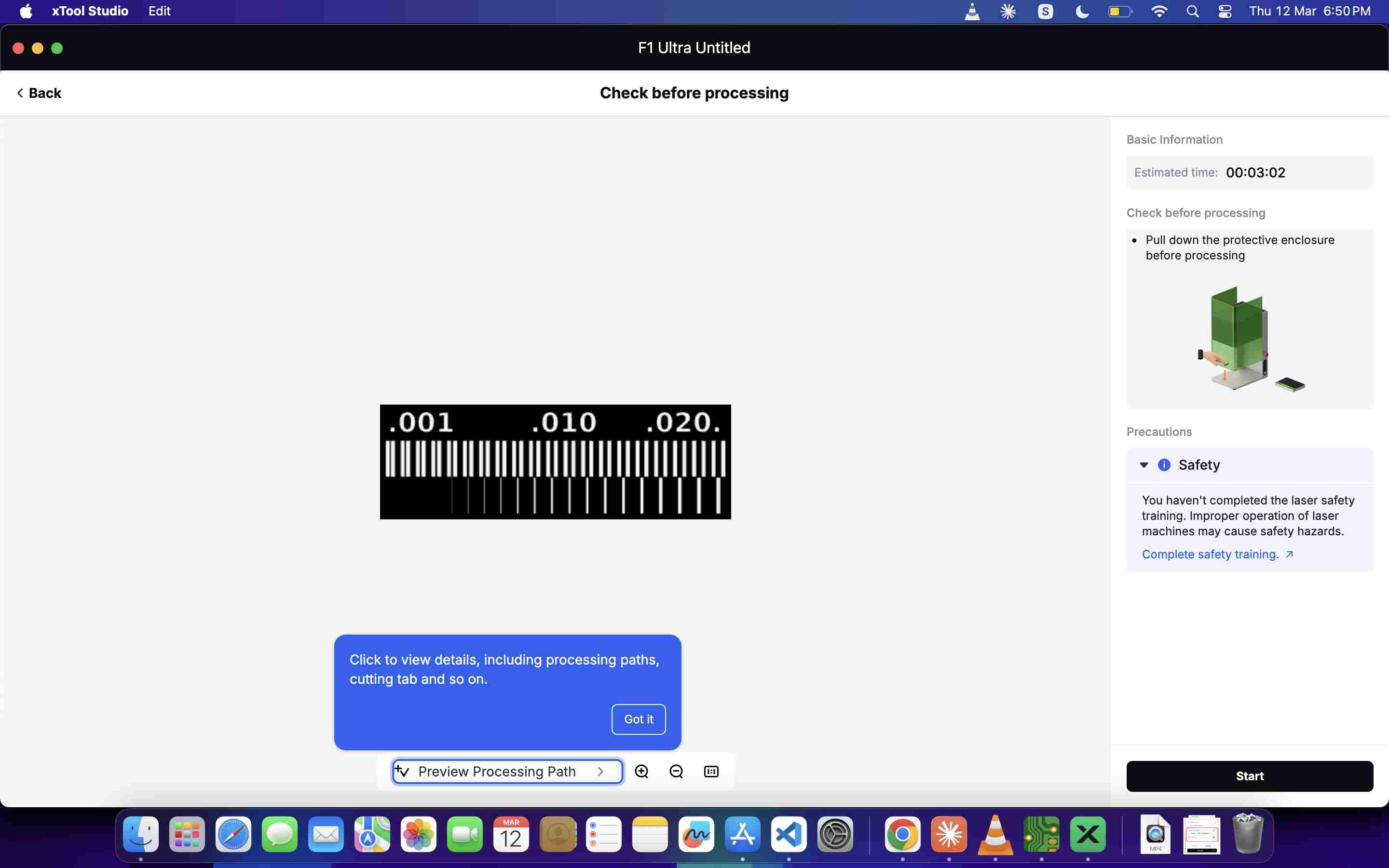
Before starting the process., we used the Framing option to preview the engraving area and make sure the design was positioned correctly on the copper board
Before starting the job, check the machine status in the software. If it shows “Busy”, the Process button will not work. This usually happens if Framing mode is still active.
Uncheck or stop the Framing option and wait until the machine status changes to “Ready”. Once it shows Ready, press Process to start the engraving.
We realized we had forgotten to sand the copper clad board before engraving. While engraving, we noticed the laser beam color was different. Sanding the board helps remove oxidation and dirt, making the copper surface better for engraving.
We also found that 25–30 passes were needed to remove the copper properly, but the software allows only 10 passes at a time, so we ran the engraving multiple times to achieve the required result.
After sanding the copper clad board, we repeated the same engraving process, aligning the design on a different area of the board before running the job again.
Upload the interior PNG file, trace it, and select the Cut option.
Or copy the traced exterior vector, delete the inner lines and keep only the rectangular outline, place it on top of the engraved design, and use the Cut option to cut the board.
Cut Settings:
- Laser: Blue light
- Power: 100%
- Speed: 200
- Passes: 10
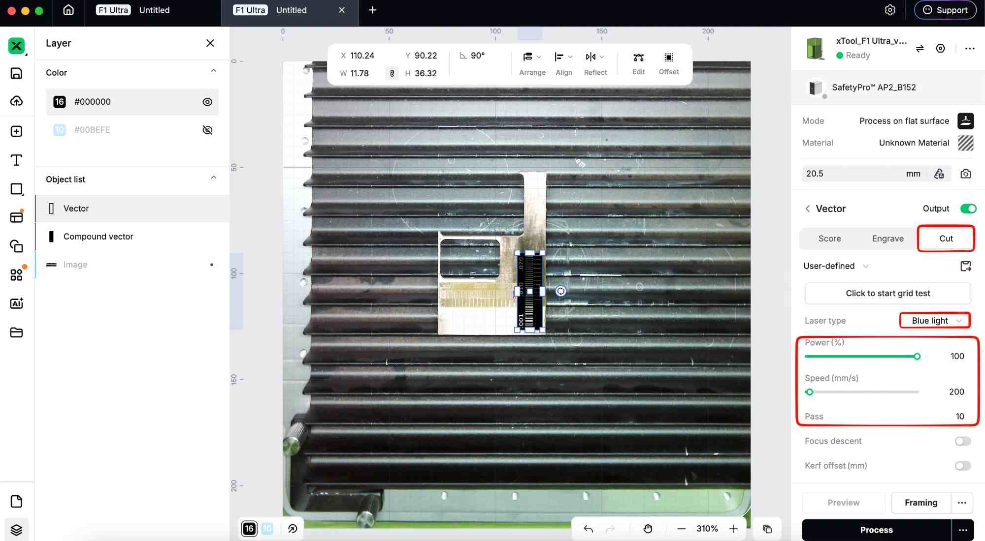
Cutting the board was not easy and did not work properly. Even after trying multiple passes, the board did not cut through. Instead, the area started turning black and leaving burn marks.
This happened because the FR-1 substrate under the copper began to burn and char due to the heat from the laser, rather than cutting cleanly through the material. 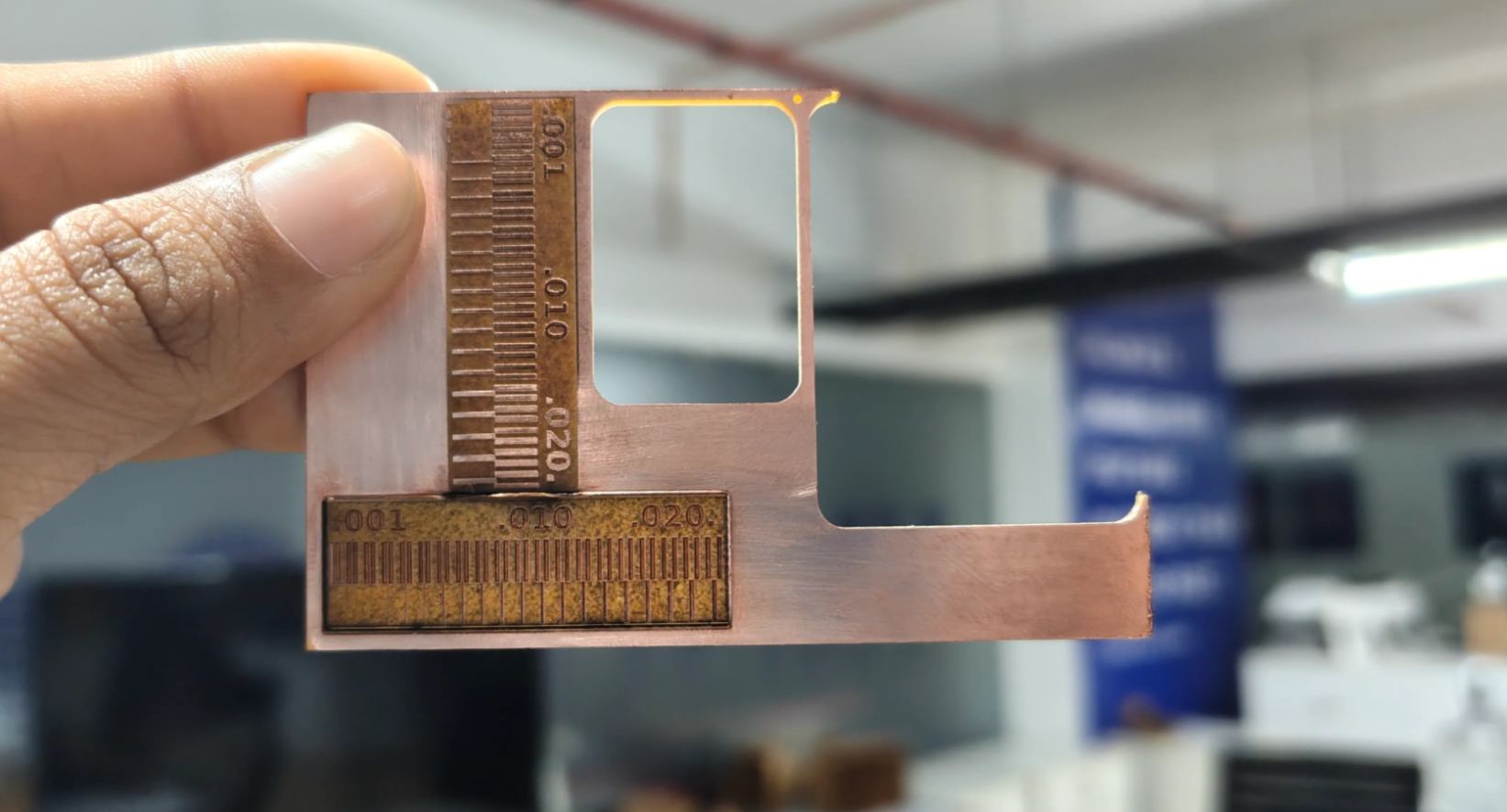
Since the board did not cut completely, we used pliers to carefully snap the edges and remove the extra material.
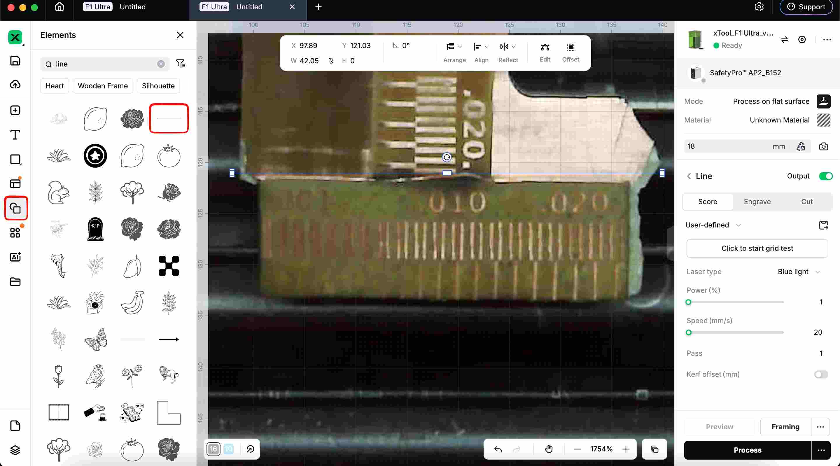
After that, in the software we used the line tool, placed a line along the edge of the board, and tried to cut along that line to clean the boundary.
Anyway, we used the pliers again to snap and clean the edges, which gave a much better result than the first attempt.
Result:
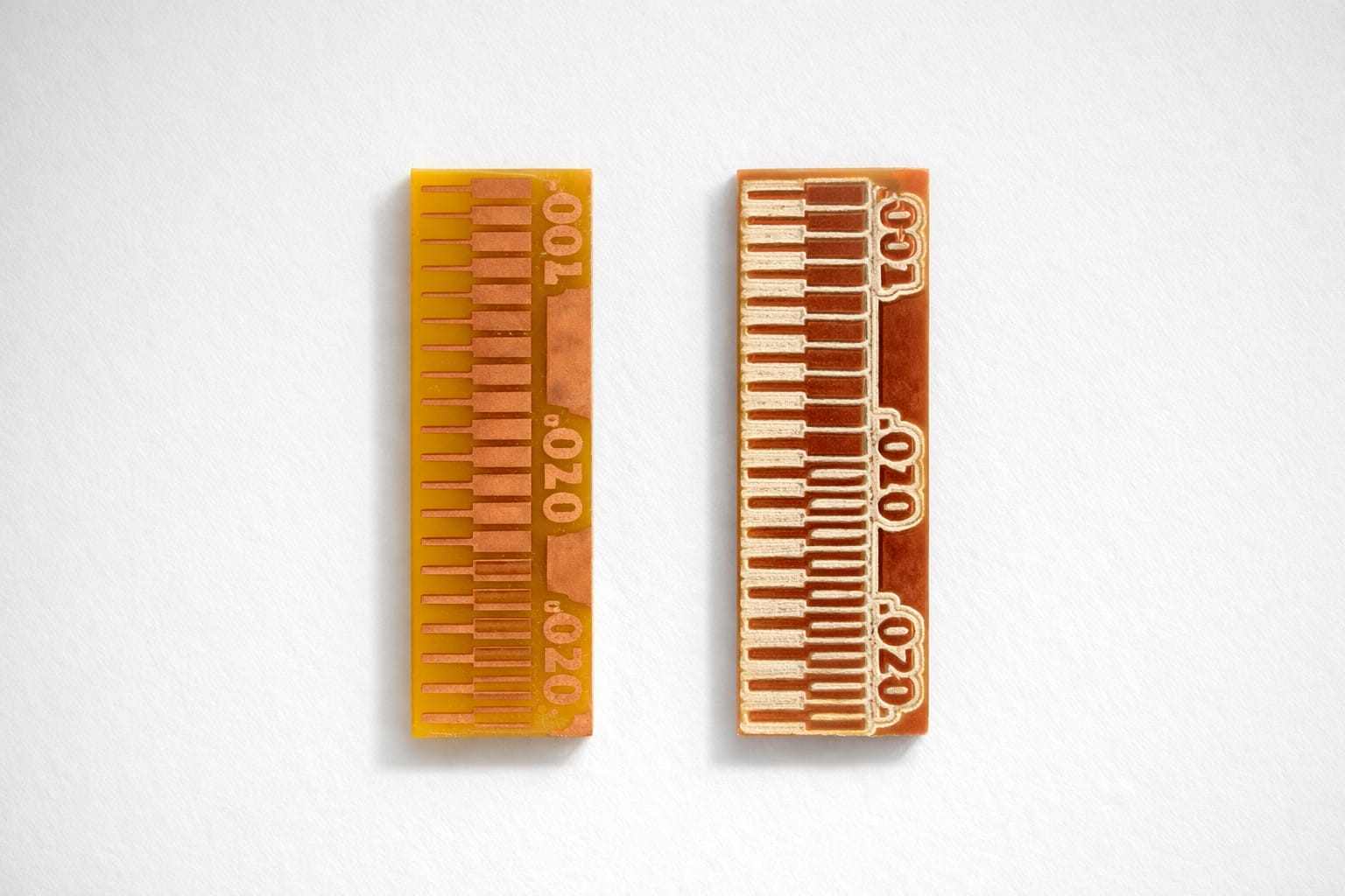
From the line test pattern, we observed:
- 0.020 inch traces → clearly visible and well isolated
- 0.010 inch traces → partially visible, some merging
- 0.001 inch traces → merged together, not distinguishable
This shows that larger trace widths work more reliably with this laser engraving workflow.
Using the xTool F1 Ultra for PCB fabrication was faster and easier than milling .The laser was able to engrave and isolate the copper traces, but cutting the board was difficult and caused burning. Overall, it works well for quick PCB engraving, but has some limitations for fine traces and cutting the board.
Flexible circuits - Abhishek , Kevin , Nadec Biju Soe
submit a PCB design to a board house - kurian
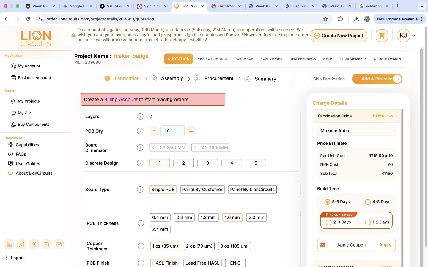
we login to the lion circuits website becasue it is an Indian board house that offered faster shipping, better local support, and overall greater convenience for our needs. so after login addded the shipping address for easy checkout process.  To send the file we needed to create a new project and add the detsils, for that click at the new project button.
 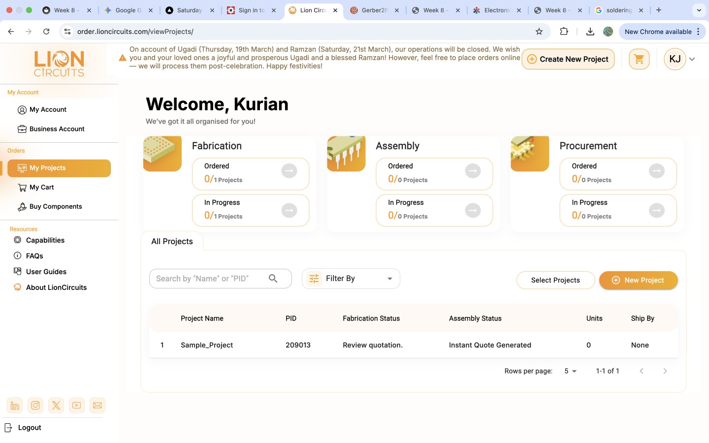 Add the detsils conected to the project including the design files.
 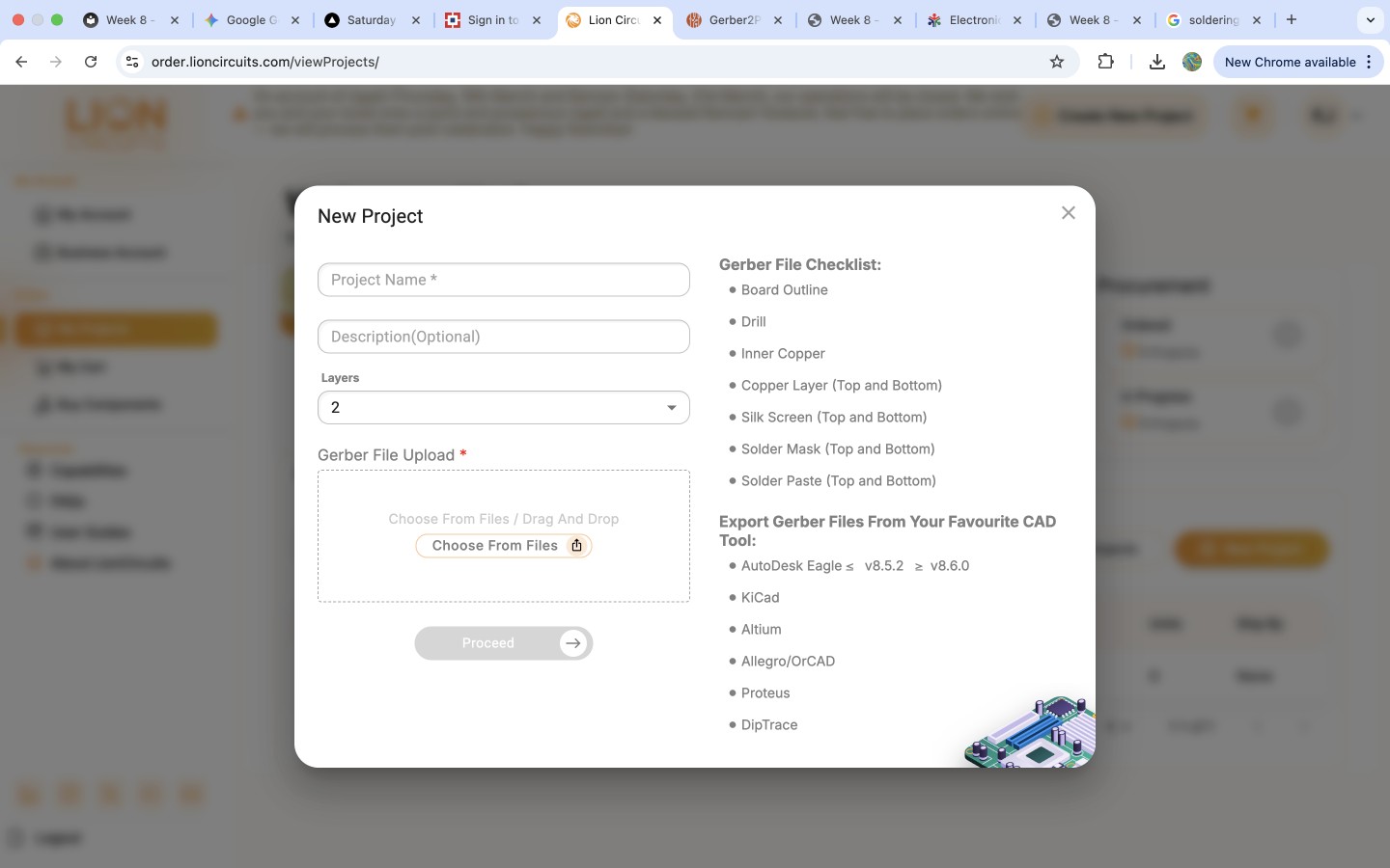 make sure that only zip files will get uploaded so compress your gerber files and upload.
 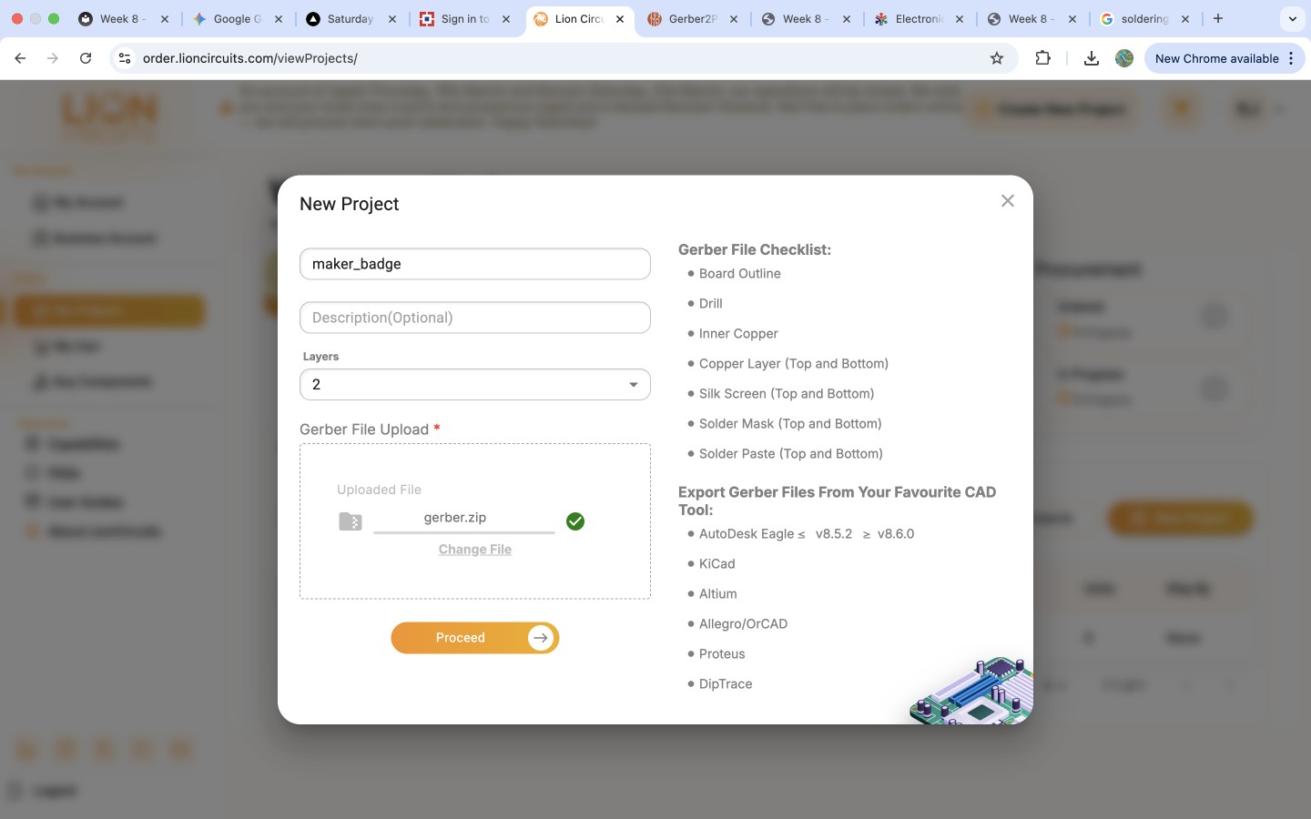 Several configuration options were available, such as board thickness, surface finish, and mask color. We selected green as the solder mask color, and the estimated price was displayed on the left panel. There was also an option for fabrication, but since we planned to fabricate the PCB ourselves in our lab, we chose to skip that step. After finalizing our selections, we clicked on ‘Add and Proceed’, which directed us to the shipping details and payment options page.