Week 8 — Electronics production
Group assignment for this week is on the Chaihuo Week 8 group assignment page. The rest of this page is my individual work.
Individual assignment
Week 8 turned the Week 6 layout into copper, then into a stuffed board on the bench. I already had schematic and routed layout; this week was Gerber export, Mods toolpaths, milling on the lab PCB CNC, soldering the XIAO ESP32-S3, and a first firmware upload.
PCB to PNG
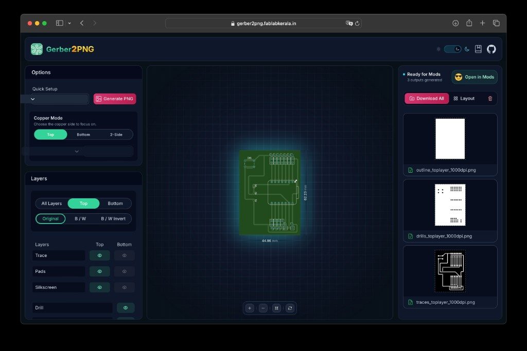
I exported F.Cu and Edge.Cuts from KiCad, then uploaded the
Gerbers to Gerber2PNG.
Mods expects high-contrast PNGs (white features on a black background), so I generated
three 1000 DPI images: traces, drills, and board outline. The preview matched the
Week 6 layout at about 45 × 62 mm before I moved on to toolpaths.
Production workflow checklist
The assessment wording mentions tool-path generation, milling or laser engraving, stuffing, debugging, and programming. My board used the milling route on copper-clad stock, not laser engraving, so I tracked the full process this way.
| Workflow step | What I did | Evidence on this page |
|---|---|---|
| Tool-path generation | Converted KiCad Gerbers to PNG and generated trace / outline G-code in Mods CE. | Gerber2PNG outputs, Mods parameters, simulation, and saved G-code screenshots. |
| Milling | Ran trace isolation first, then board outline on the KEXU PCB CNC. | Machine setup photos, zeroing photo, milling video, and final milled board photo. |
| Stuffing | Soldered the XIAO ESP32-S3 and then added the off-board harness wires. | Soldered XIAO and wire-harness photos. |
| Debugging | Found a lifted 3.3 V trace and changed the power path for the encoder branch. | Damage photo and explanation of the AMS1117 workaround. |
| Programming | Uploaded pcb_testing.ino and verified the W8 SYSTEM screen. |
Firmware test video and downloadable Arduino sketch. |
Toolpaths in Mods CE
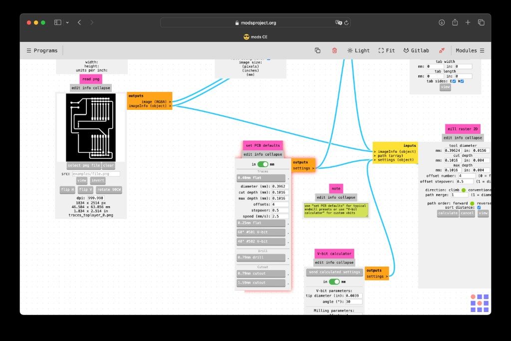
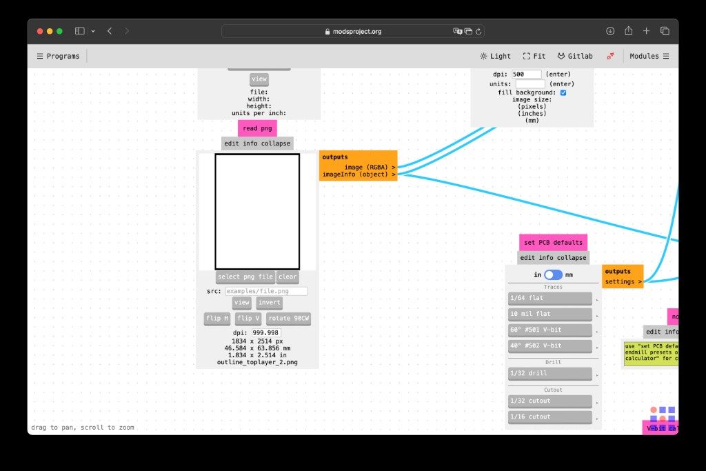
I used the G-Code Mill 2D PCB workflow at
modsproject.org.
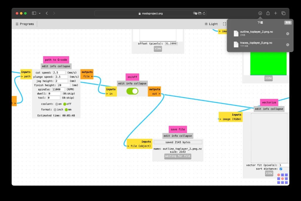
Trace isolation and board outline are separate programs: different PNG inputs, different
passes, and separate .nc files loaded on the machine one at a time.
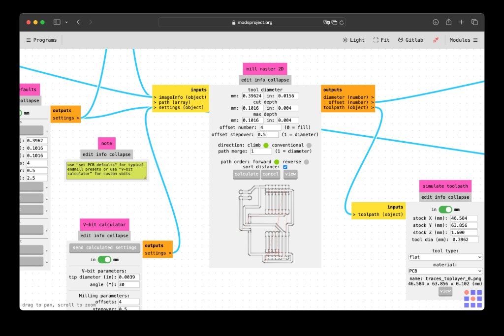
For traces I loaded traces_toplayer_0.png and chose the
0.40 mm flat preset: 0.102 mm cut depth, four isolation offsets
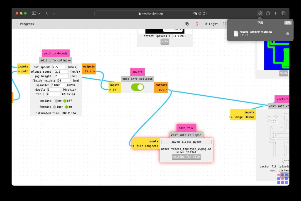
at 0.5 stepover. I simulated the path in Mods before posting; the estimate was about
31 minutes at 2.5 mm/s feed and 11 000 rpm spindle speed. Output:
traces_toplayer_0.png.nc.
For the outline I loaded outline_toplayer_2.png, ran a contour program with
the same flat end mill, and saved outline_toplayer_2.png.nc with matching
feeds and spindle speed.
Milling
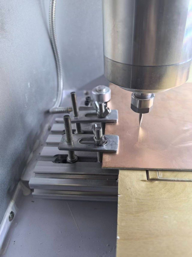
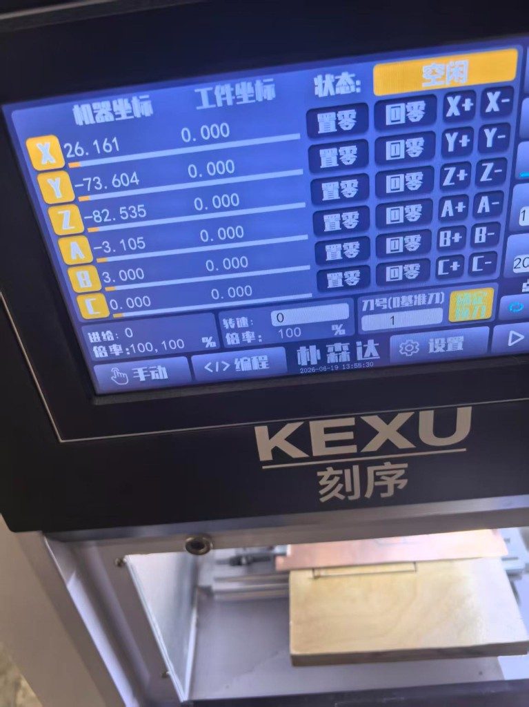
On the lab KEXU PCB mill I clamped single-sided copper-clad stock on the spoil board, touched off XY/Z zero on the controller, and ran the trace file first. I stayed at the machine for the full isolation pass, swapped to the outline program, and re-checked zero before cutting the board free. Flat stock and a firm clamp matter here; any flex shows up as uneven isolation depth.
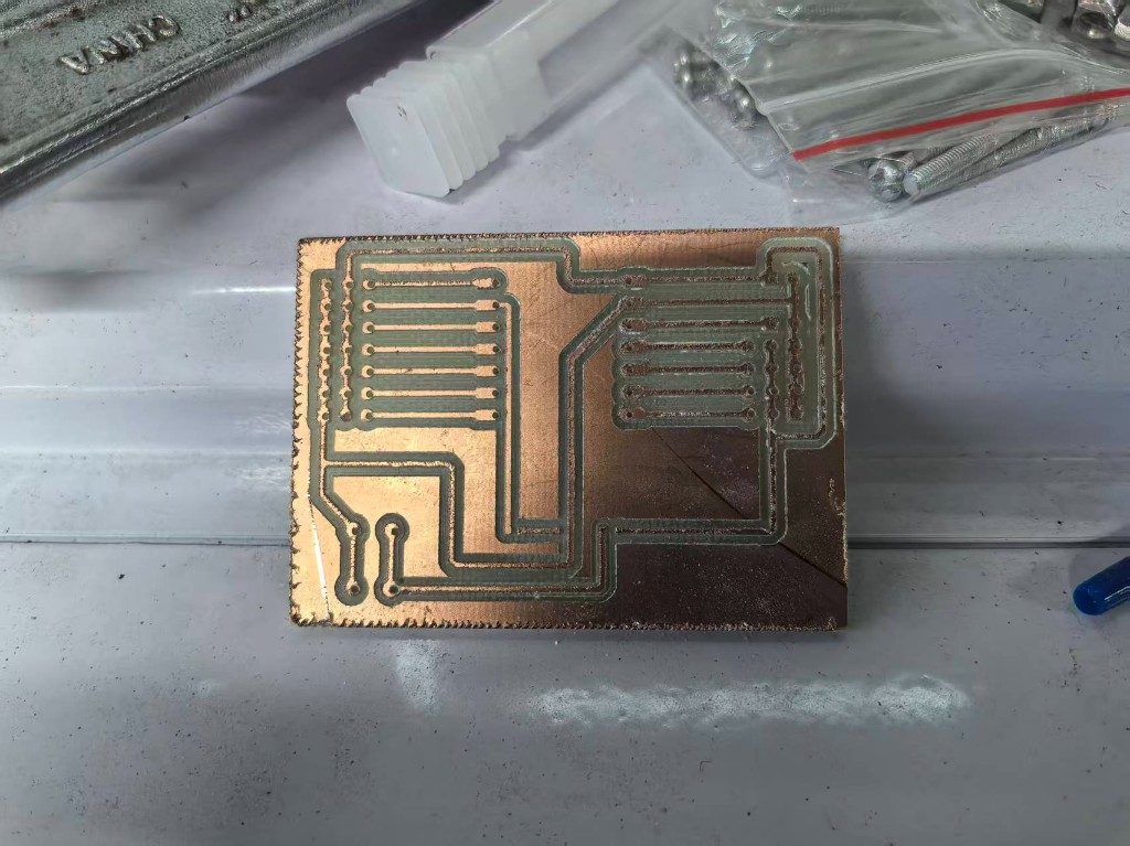
After vacuuming copper dust off the bed I deburred the edges and checked isolation between traces with the naked eye. The milled board matches the Week 6 layout: XIAO footprint in the centre, 1×3 header rows along the sides, and SW1 at the top edge.
Stuffing and soldering
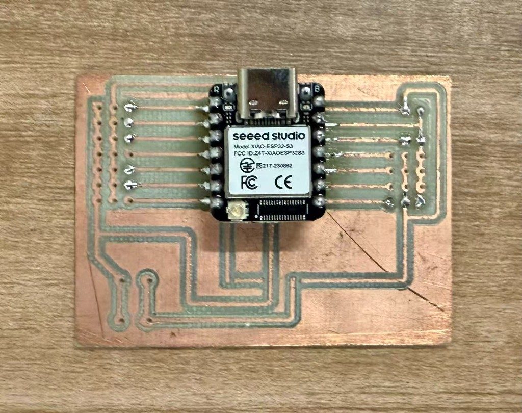
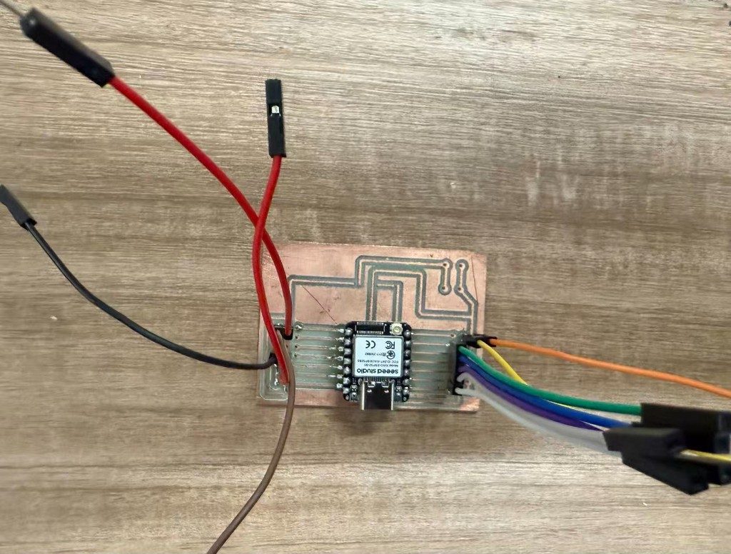
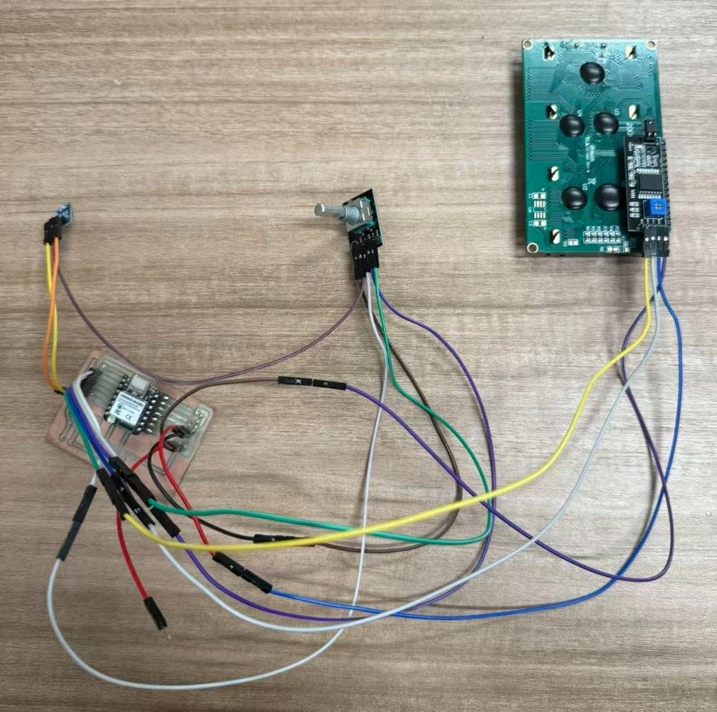
I soldered in a fixed order: XIAO first, then harness wires to the encoder and LCD nets, then off-board modules on jumpers so I could debug without desoldering the module. The castellated XIAO pads are tight. Flux and a narrow tip helped, but this step still took longer than breadboard wiring.
Problem: lifted 3.3 V trace
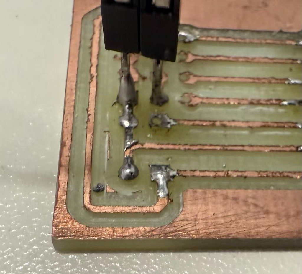
While soldering a header I overheated one area and lifted part of the on-board 3.3 V distribution. I could no longer rely on the PCB pad to feed the rotary encoder, so the encoder branch runs from a separate AMS1117 module instead. The wiring change is documented on the input-device page.
Bench bring-up
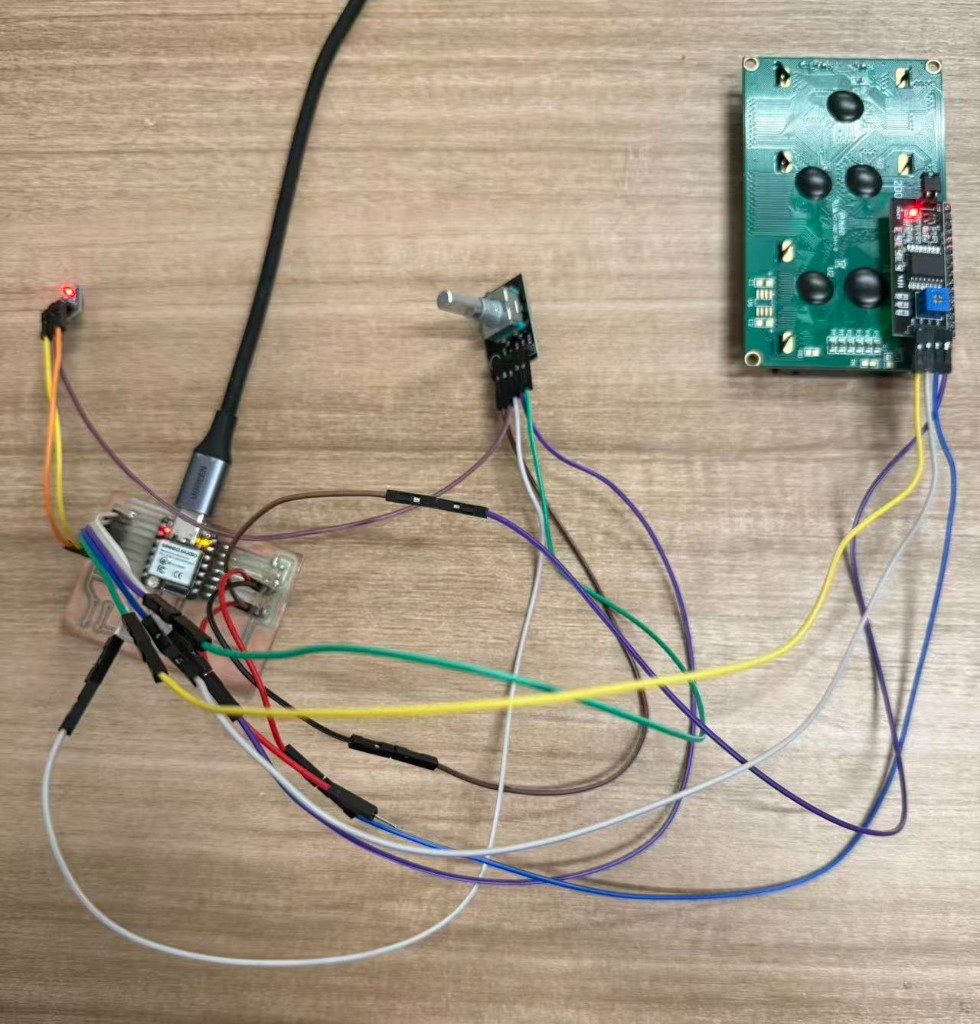
With the encoder, LCD backpack, and regulator connected, the stack matches the harness plan
in pcb_testing. USB powers the XIAO; the encoder uses the external 3.3 V
regulator. This is the board I programmed for assessment — milled, stuffed, and running
custom firmware.
W8 SYSTEM: firmware test
Once the sketch is uploaded it lands on the W8 SYSTEM page. Line 1 shows the
page name; line 2 prints uptime (t…s) and the LCD backpack I²C address in hex. That
confirms the XIAO is running, I²C init succeeded, and the display responds.
Download Arduino sketch (pcb_testing.ino)
Reflection
Simulating in Mods before touching copper caught at least one polarity mistake. On the machine, zeroing and clamping weighed as much as the KiCad layout. Bump the origin between trace and outline files and the cuts mis-register. Hand soldering on milled copper is less forgiving than a breadboard: one lifted trace changed how I powered an input device until I could respin.
Following the group PCB milling checklist (clamp clearance, tool diameter match, touch-off, deburr before inspection) made the solo run boring in a good way. Next revision: widen the 3.3 V pour and enlarge pads before milling again.