Week 6 — Electronics design
Group assignment for this week is on the Chaihuo Week 6 group assignment page. The rest of this page is my individual work.
Individual assignment
KiCad carried most of this week: a development board around the Seeed Studio XIAO ESP32-S3 with local input and output, GPIO broken out on pin headers, and USB for power and serial to a host.
Board design plan
The board is a general-purpose XIAO breakout with two simple I/O circuits for assignment testing. Most signals route from the module to 1×3 headers in a consistent pin order so jumper wires can reach breadboard peripherals without re-reading the schematic each time.
| Block | Reference | Role |
|---|---|---|
| Microcontroller module | U1 | Seeed XIAO ESP32-S3 on castellated pads; USB for power and serial. |
| External power input | J1 | 1×2 header for +5 V and GND when not powered from USB. |
| GPIO breakout | J2–J12 | 1×3 headers (GND, +5 V, signal) tied to module pins. |
| Extra connector | J13 | 1×2 header for an additional signal pair. |
| Button input | SW1 + R1 (1 kΩ) | Tactile switch on /L1 (GPIO1) with pull-up to +5 V. |
| LED output | D1 + R2 (220 Ω) | Indicator on /L2 (GPIO2) with current-limiting resistor to GND. |
Schematic
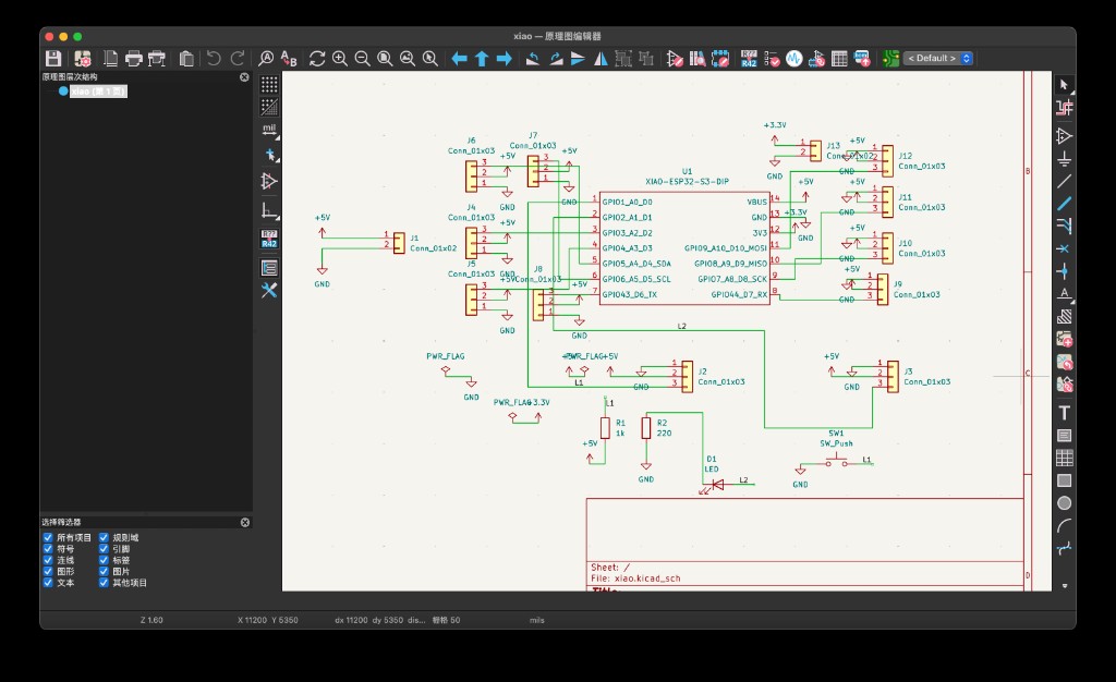
I had not used KiCad regularly before this week, so the schematic stage was mostly learning
the editor: symbol placement, wiring, net labels, and the shortcut workflow for moving
between tools. The Seeed XIAO ESP32-S3 symbol and its matching footprint are not in KiCad’s
default libraries. I installed the
Fab Academy KiCad library
and added the Seeed Studio footprint table so KiCad could resolve
Seeed_Studio_XIAO_Series:XIAO-ESP32-S3-DIP before I moved to PCB layout.
After the symbols were on the sheet, I wired power flags and PWR_FLAG markers
on the +5 V, +3.3 V, and GND nets so the electrical rules check would treat them as driven.
The button uses an external pull-up because the switch ties /L1 to ground when
pressed. The LED and its 220 Ω resistor sit on /L2 so a logic high turns the
indicator on.
PCB layout
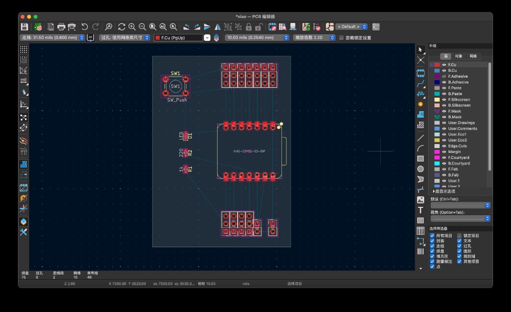
I pushed the schematic into the PCB editor with Update PCB from Schematic. All footprints arrived as a pile connected by ratsnest lines. The layout strategy was:
- Place the XIAO footprint near the center because most nets terminate there.
- Put the 1×3 headers on the top and bottom edges for cable access after assembly.
- Keep SW1, R1, D1, and R2 close to the module pins they use so button and LED traces stay short.
- Draw a rectangular outline on
Edge.Cutsand stay inside roughly 46 × 62 mm. - Route everything on the front copper layer only; this board is a single-sided milled PCB with no vias.
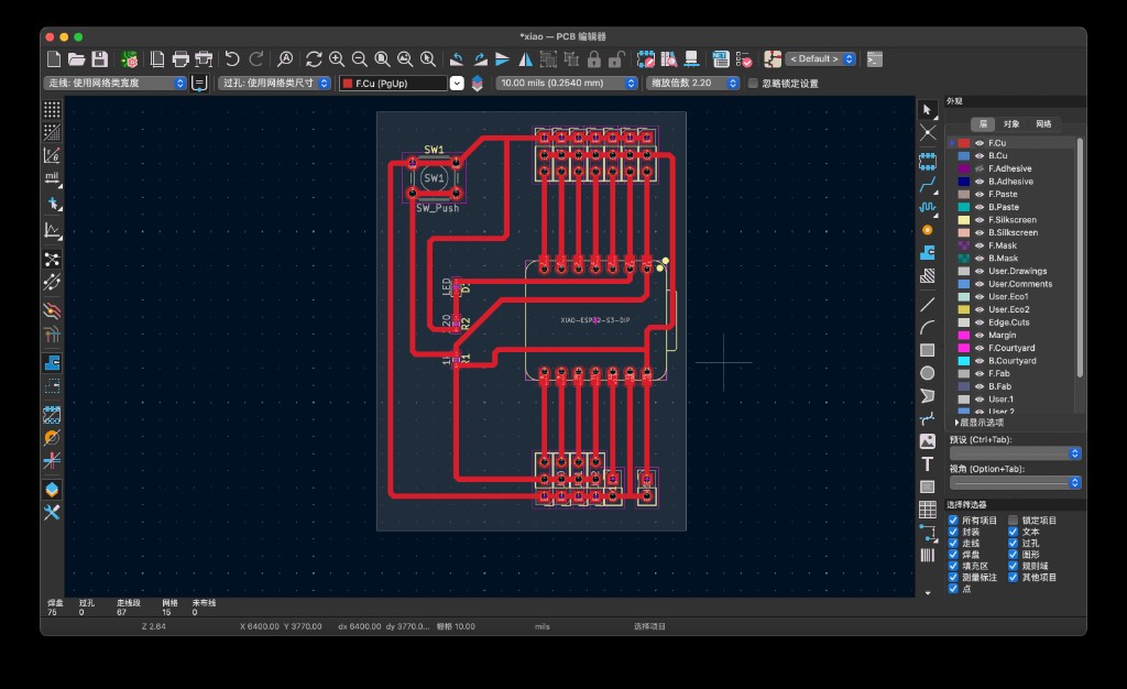
Because we mill boards in-house rather than ordering a two-layer PCB, I treated trace width
and spacing as part of the design specification. I routed signal traces at
0.8 mm (about 31.5 mil) on F.Cu, kept a
0.5 mm copper-to-edge clearance, and packed headers tightly but left enough
gap for the 1/64 inch end mill used in our lab workflow. Wider traces are less likely to
break during milling and are easier to inspect under the microscope afterward.
| Parameter | Value |
|---|---|
| Board outline | ≈ 46.0 × 62.2 mm |
| Board thickness | 1.6 mm (default) |
| Copper layers used | Front only (F.Cu) |
| Signal trace width | 0.8 mm |
| Minimum DRC track width | 0.2 mm |
| Copper edge clearance | 0.5 mm |
| Vias | 0 (single-sided design) |
| Routed nets | 15 |
| SMD passives | R1, R2 in 0603 |
| Through-hole parts | SW1, J1–J13 |
Problems and fixes
Missing XIAO library. The first blocker was footprint availability. Until the Fab Academy library was installed, KiCad could place the schematic symbol but not assign a valid board footprint. Installing the published KiCad library fixed that and matched what other students in the lab use for XIAO boards.
Single-sided routing constraints. With only F.Cu available, every
net has to find a path without crossing another trace. I repositioned the header row several
times to reduce ratsnest tangles, then chose 0.8 mm width as a conservative setting for our
PCB mill. Narrower traces would have left more room but were easier to damage during
machining.
Split button net. My first routed version left /L1 in two
separate copper islands between the button circuit and the XIAO GPIO1 pad. DRC reported one
unconnected item. I added the missing trace segment, re-ran DRC, and the net cleared with
zero unconnected items.
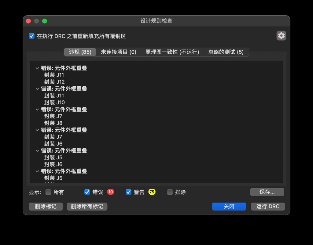
Dense header courtyards. Packing twelve 1×3 headers along both edges triggered courtyard-overlap warnings in DRC. The electrical routing is valid, but I plan to nudge connector placement before milling in Week 8 — Electronics production so the physical board has more clearance between adjacent headers.
Design rule check
After the routing fix, KiCad DRC reported zero unconnected items. I still have courtyard overlap warnings on adjacent headers, which I am tracking for the milling revision, but the electrical connectivity check passed.
Fabrication
The physical board was not milled during Week 6. The fabricated board hero shot and milling results are documented in Week 8 — Electronics production.
Design files
Download KiCad project files (.zip)
Archive includes xiao.kicad_sch, xiao.kicad_pcb, and
xiao.kicad_pro.
Reflection
Schematic through DRC was a full KiCad pass for me. The biggest lesson: read the XIAO pin map and install the correct library before placing connectors, because header positions drive trace length on a single-sided board. During the group measurement session I also saw that probe ground placement and meter range selection matter as much as firmware when matching a scope trace to board behavior.
Logic-analyzer screenshots live on the Week 9 group probing page, not here. Even so, the DMM continuity checks and scope shots in Week 6 already showed which nets were at 3.3 V before I milled the layout in Week 8.