Week 06 – Electronic Design
Han Ferik
Weekly Assignments:
Check Out Our Group Assignment
Group assignment:
Use the test equipment in your lab to observe the operation of a microcontroller circuit board (as a minimum, you should demonstrate the use of a logic analyzer)
Document your work on the group work page and reflect what you learned on your individual page
Individual assignment:
- Use an EDA tool to design a development board that uses parts from the inventory to interact and communicate with an embedded microcontroller
Getting Started with KiCad
Importing The Fab Library
Before we get started to designing our PCB, let’s first download the Fab Library, which will asist us while building our PCB.
In order to import the library into our project. Lets first create a new project.
Before looking over the left bar of the app. First, create a new folder specifically for KiCad, that you will use to locate the new project that you will build. Later, click on the element that says “New Project”, or either use “Control + N”.
After that, it opens a new folder creation page. There, name your project (I named Week 6 PCB) into your liking and save it inside the folder that you have created beforehand, which was specifically for KiCad.

After that you need to download the Fab Academy KiCad Library file. You can reach to that file through the link below:
After you downloaded that file, you need to extract that file with including everything in that file.
When you finish that, there are two options for you to left in order to import the library. You either need to find and copy the pathway of the file named “fab.kicad_sym”.

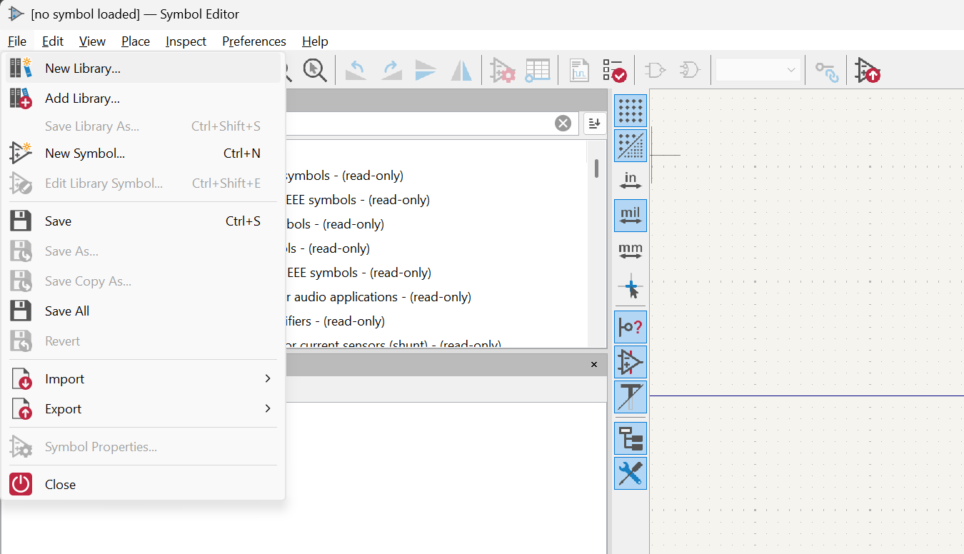
Once that’s done. You need to open up the “Preferences” from the horizontal bar at the top at KiCad, and you need to choose “Manage Symbol Libraries…”.

When you chose that, it takes you into a new window. Here, you need to go down to the bottom, and there you need to click on the “+” sign to add a new file inside the project. That creates a new tab inside those file. Right now is the the other option. You can also click to the “folder icon”, and find your file throughout your computer rather than copying the file path that we copied before. This is shown in the photo below.

But, if you still insist on using the pathway, you can directly paste it to the text box on the left of the folder icon, which is named “Library Path”
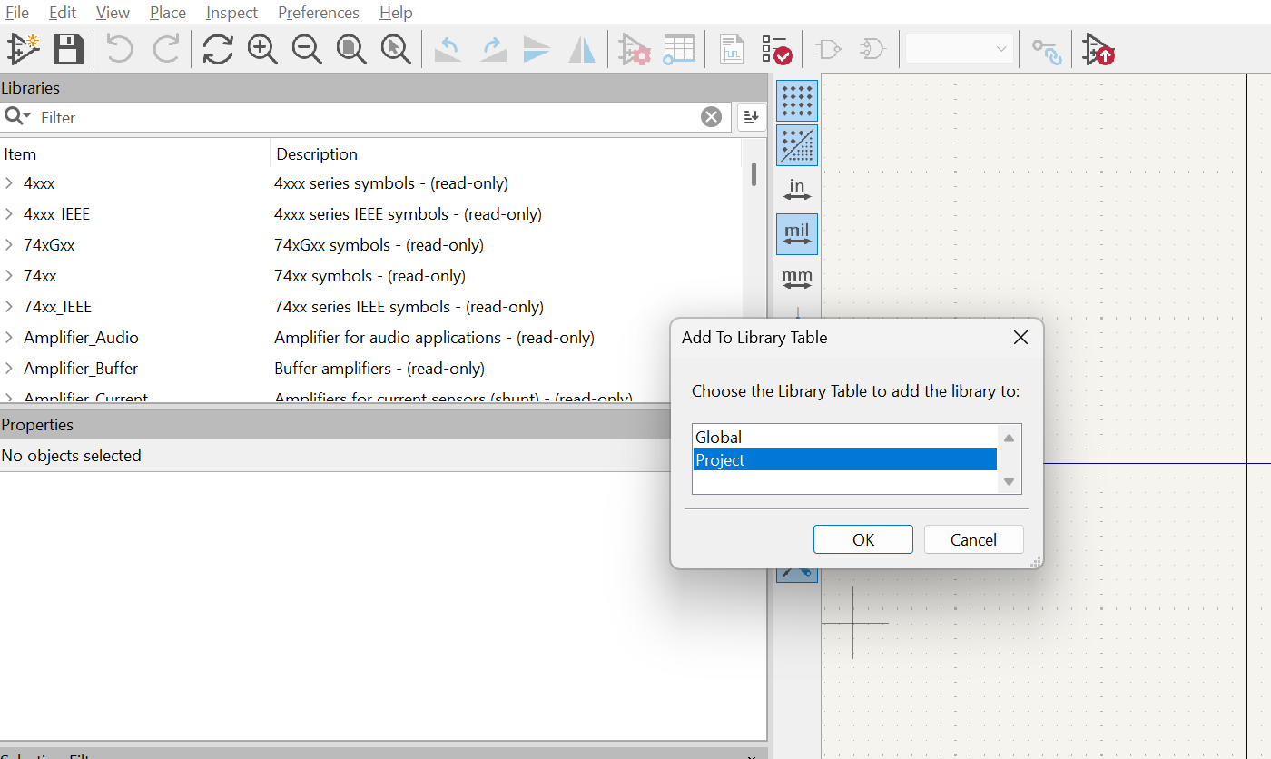
After concluding either options, make sure that the check boxes on the left are checked. Also, name the file on its “Nickname” text box, which I named it as “fab”.
Now, click “Okay”, and our process for this library is done.
Here is also a YouTube video, which you can utilize during the process:
KiCAD Fab Academy Library Install Clip
Again, you also need to add a Footprint Library. So, with applying the same steps provided above. You need to open up the “Preferences” from the horizontal bar at the top at KiCad, and you need to choose “Manage Footprint Libraries…”.
Here you need add “fab.pretty” as footprint library. And, once you add it, this library will also be imported. Again, make sure that the check box on the left is checked. Also, name the file on its “Nickname” text box. Here, I again named it “fab”

Finally, You need to go to the “Preferences” from the horizontal bar at the top at KiCad, and you need to choose “Configure Paths…”. In order for 3D models to load correctly, we need to add our Fab Library path to KiCad. So, here, you need to add new environment variable called “FAB” that points to location of the fab library on your drive. You can see an example of mine in the image below:

Click “Okay”, and we are set.
Schematic Editor
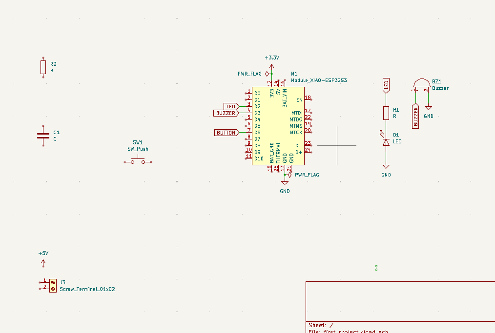
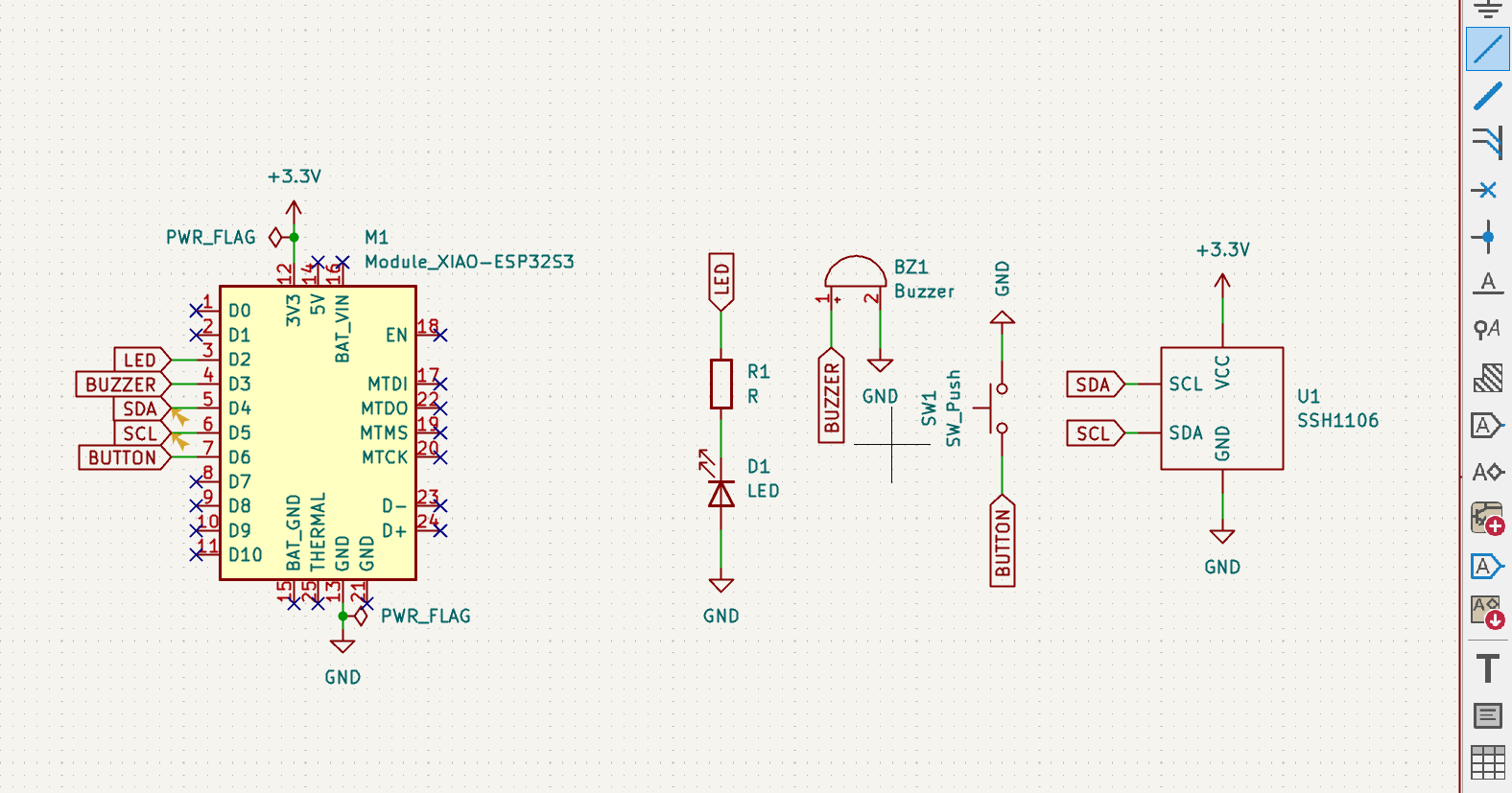
Wiring the ESP32S3 With The Inputs and Outputs
For the Inputs and Outputs, I used Fab and General Library of KiCad.
I uploaded the Inputs and Outputs that I am going to use.
Here is an example of what I did, but there is different components.
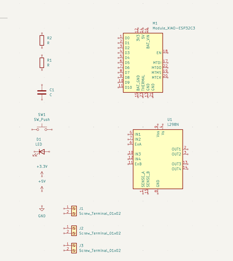
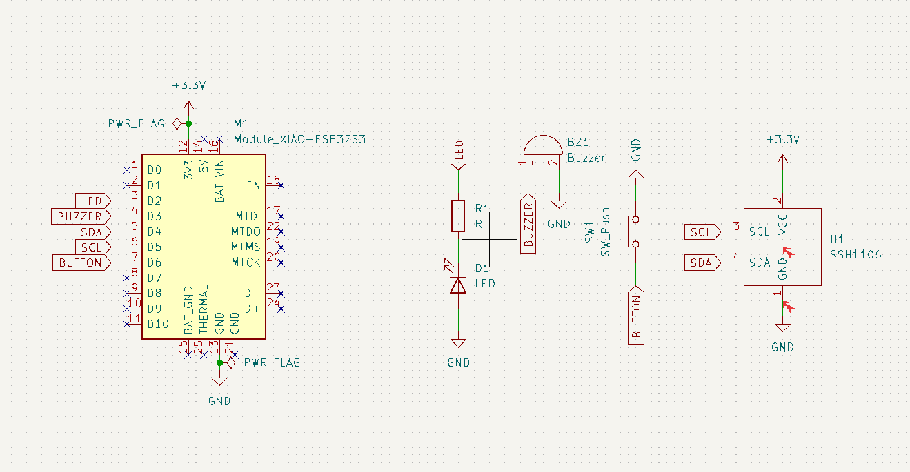
After that, I used the wiring based on my final project wiring that I made on Breadboard with ESP, on which the wirings were tested and working.

I used labels for the pins that I am going to wire the components with to the ESP.
I connected those label to the right ends of each component. And, I also wired GND for the components that I used GND on my Breadboard.
I also used a resistor for the LED.
My progress looked like this picture below.
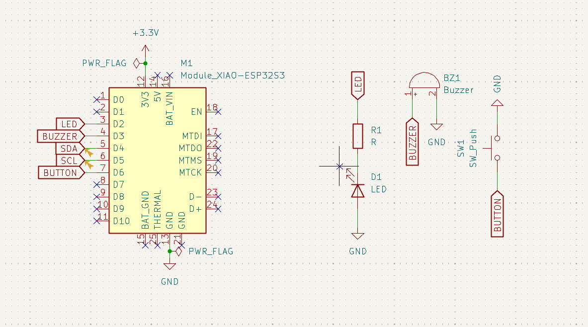
In the end my wiring looked like below.
Symbol Editor
Creating Custom Symbol
Since I couldn’t find a symbol for an Oled Screen. I went through to create that symbol myself.
I launched Symbol Editor in KiCad.
I clicked File and New Library.
I selected Project.
I wrote the name of the library. And, saved.
After that, it created a new library.
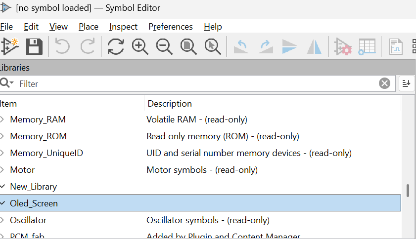
I right clicked that new Oled Screen library, and clicked New Symbol.
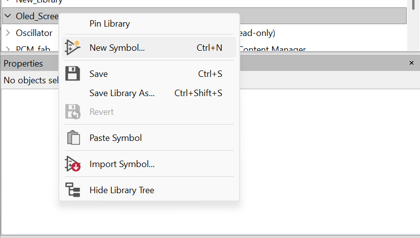
I named it as 1.3 Inch OLED SSH1106.
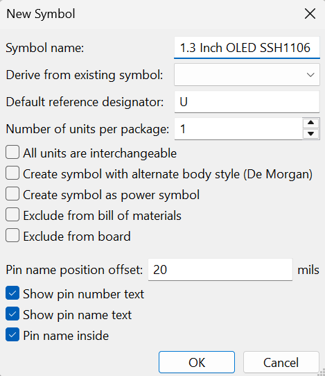
Then, I clicked OK.
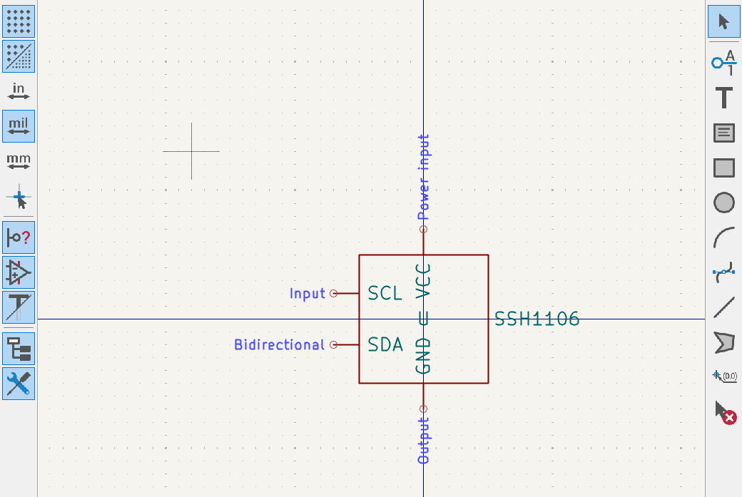
I draw a rectangle.
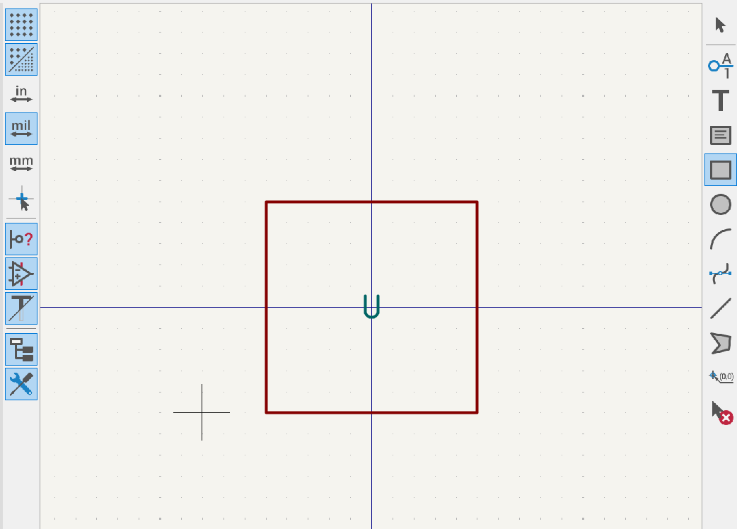
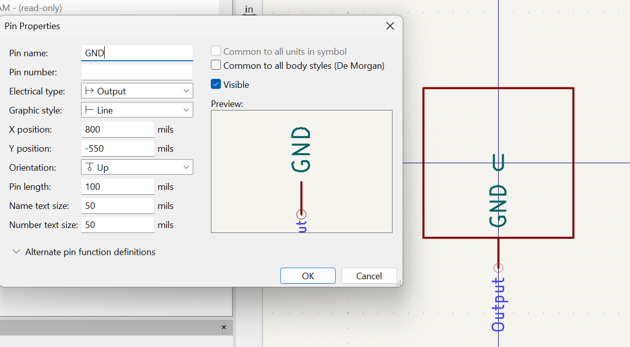
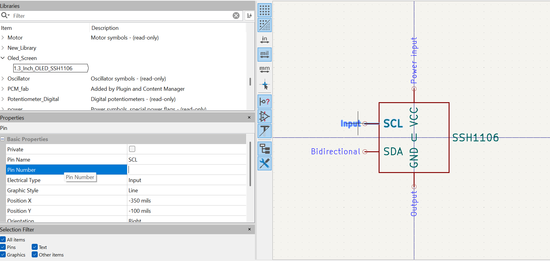
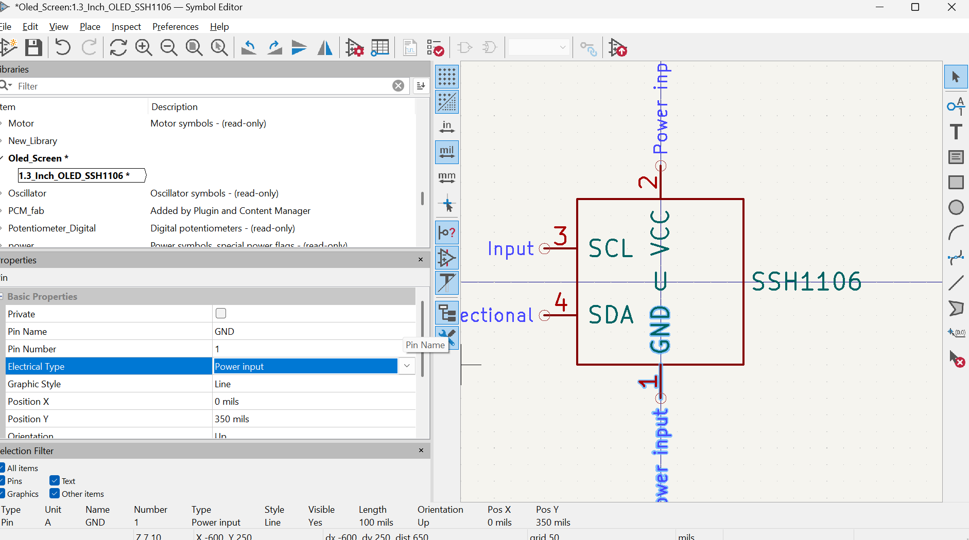
I clicked Draw Pins, and added every pin on my OLED Screen to the rectangle.
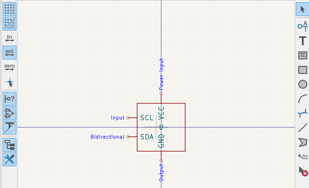
Be careful with choosing the Pin Properties. For example, Ground GND should be selected as Output.
Select VCC as Power Input.
Select SCL as Input.
Finally, Select SDA as Bidirectional.
Now, right click on the tray.
Click on Symbol Properties.
On Value, write SSH1106.
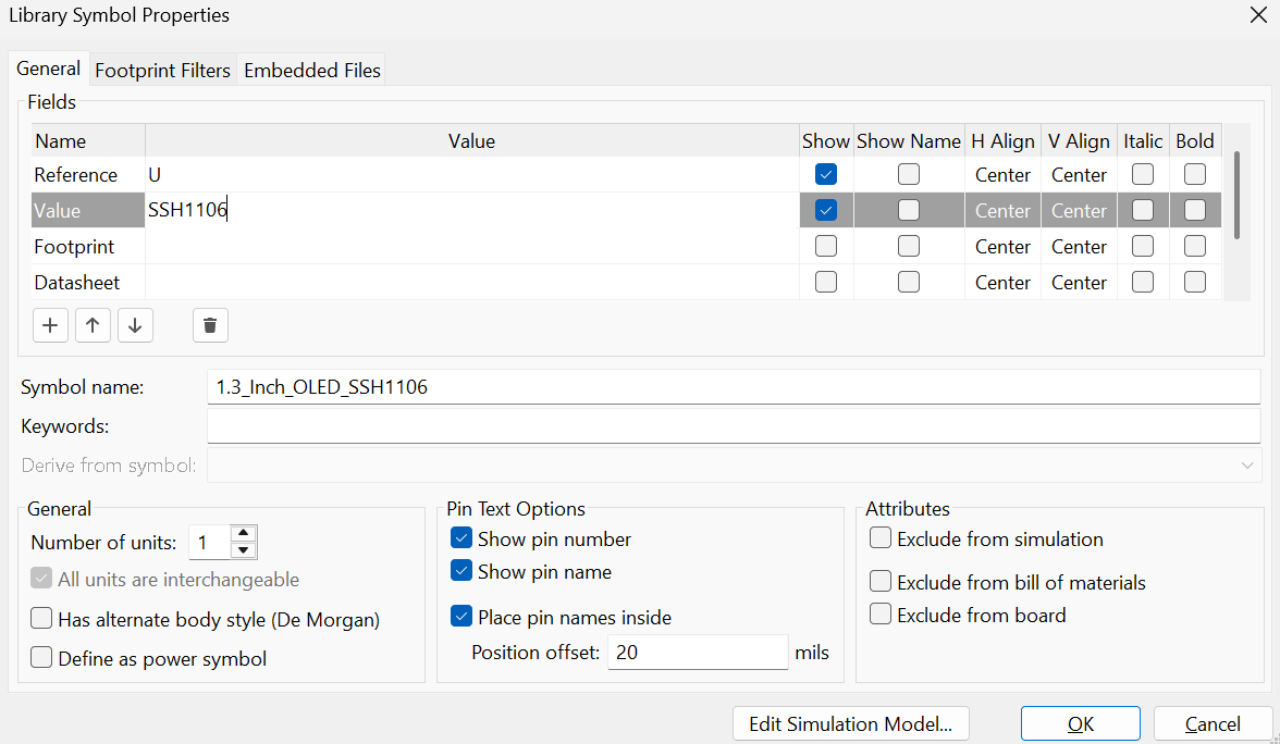
Click OK.
Move the SSH1106 Value to the right of the Rectangle.
After that, Go back to your Schematic.
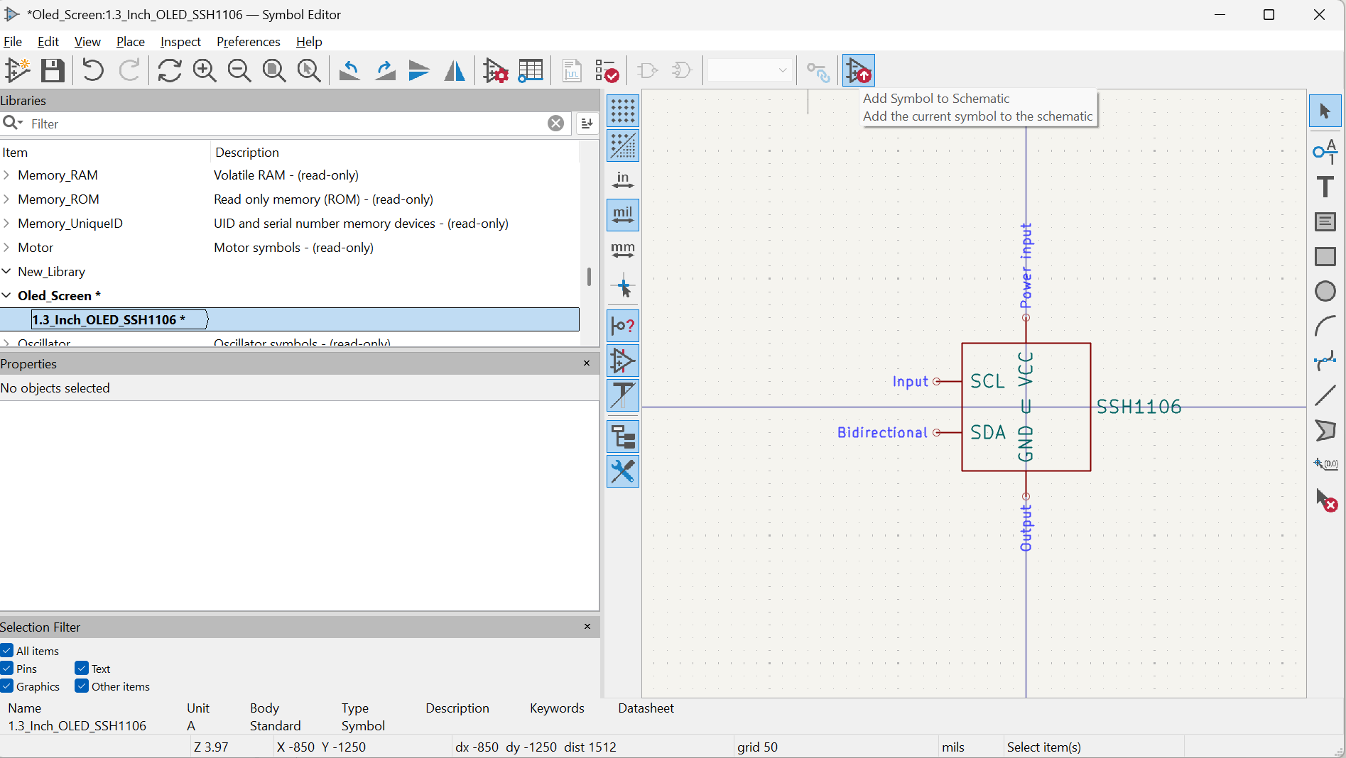
Click on Add Symbol to Schematic.
And, Select the part that we made just before, and upload it.
Schematic Editor
Going Back To The Wiring
I wired the labels, GND, and VCC of the OLED Screen with the Draw Wires Tool.
And, my final look was like this.
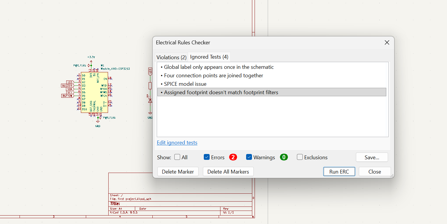
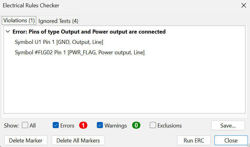
Now, I clicked on Inspect, and checked my design with Electric Rules Checker.
And, it gave 2 errors. I realized that this was because I didn’t add pin numbers to my custom part design.
Symbol Editor
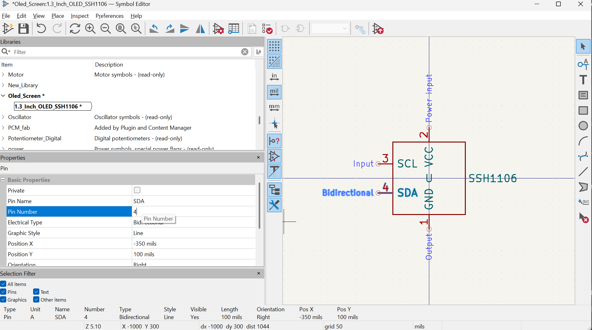
Adding Pin Numbers
So, I went back to , and added pin numbers to the custom part.
I have added all pin number, and it now looked like this below.
Schematic Editor
Organizing the Setup
I deleted the old OLED part, and uploaded the new one at its old place.
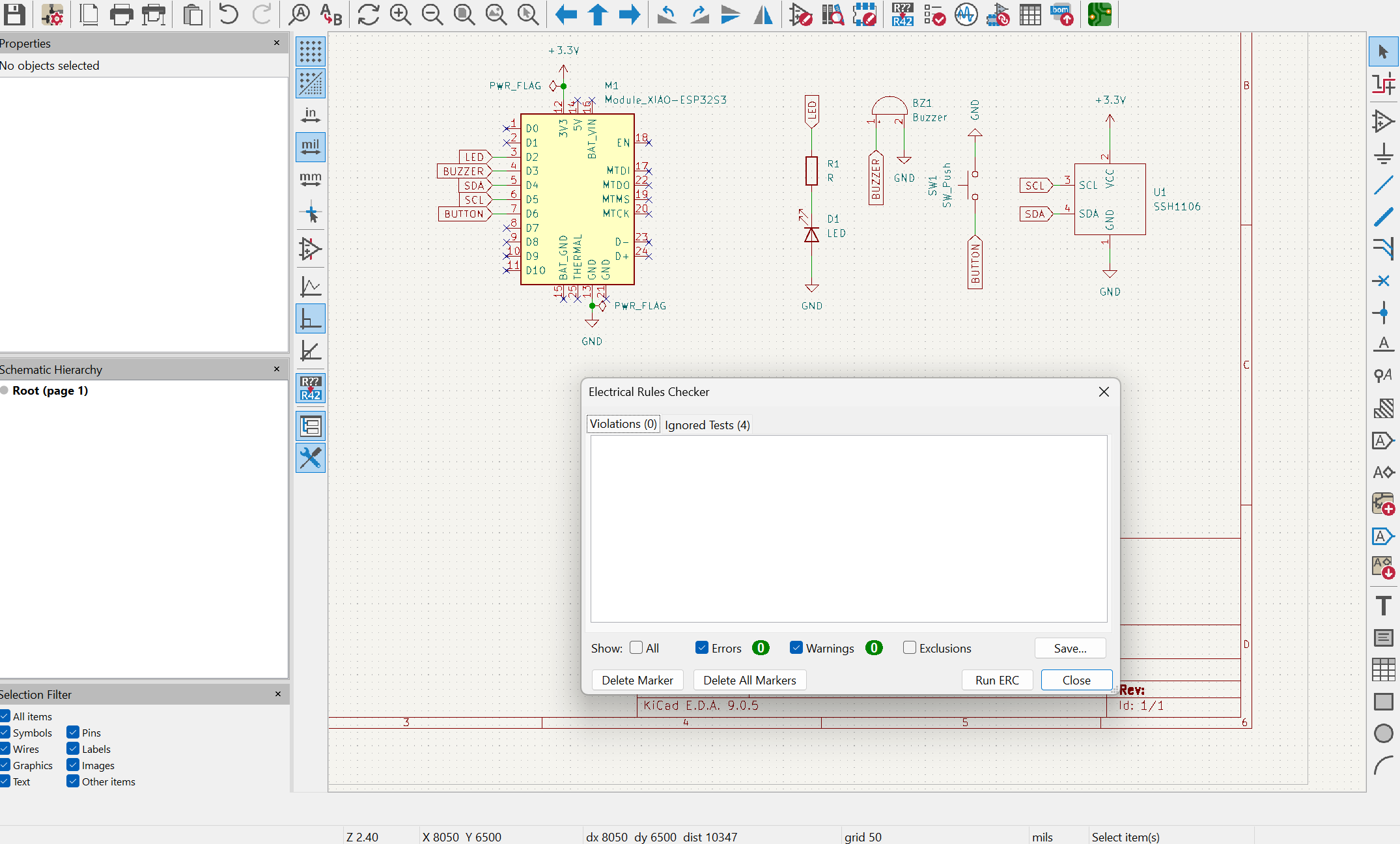
I again checked my design with Electric Rules Checker.
It again gave an error because I wrote Output for Ground.
Symbol Editor
Changing the Ground Output
I again opened up the Symbol Editor.
Clicked on GND.
I changed Electrical Type into Power Input.
Schematic Editor
Finalizing The Parts
I deleted the old OLED part, and uploaded the new one at its old place.
I again checked my design with Electric Rules Checker.
And, now we were clean.
Footprint Editor
Creating a Footprint For My OLED Screen
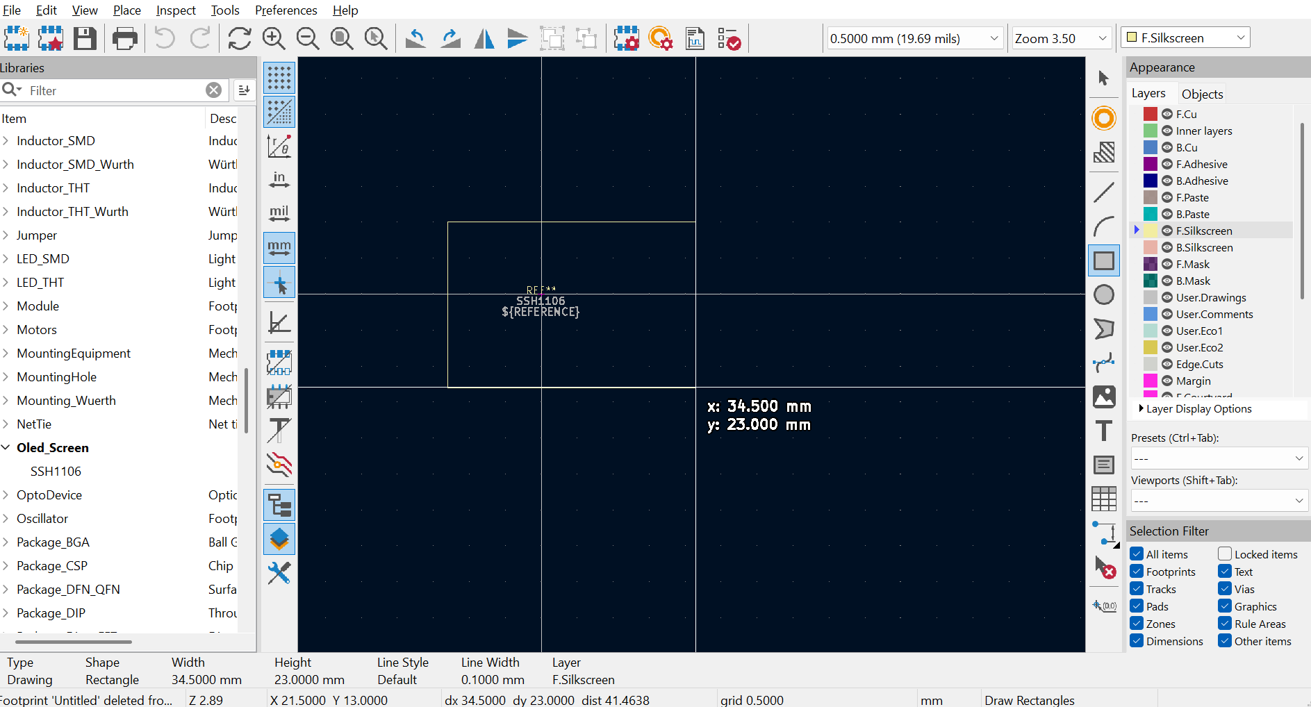
Now, I need to create a new footprint for the OLED Screen.
So, my 1.3 Inch OLED Screen’s measurement of the sides is 34.5mm x 23mm.
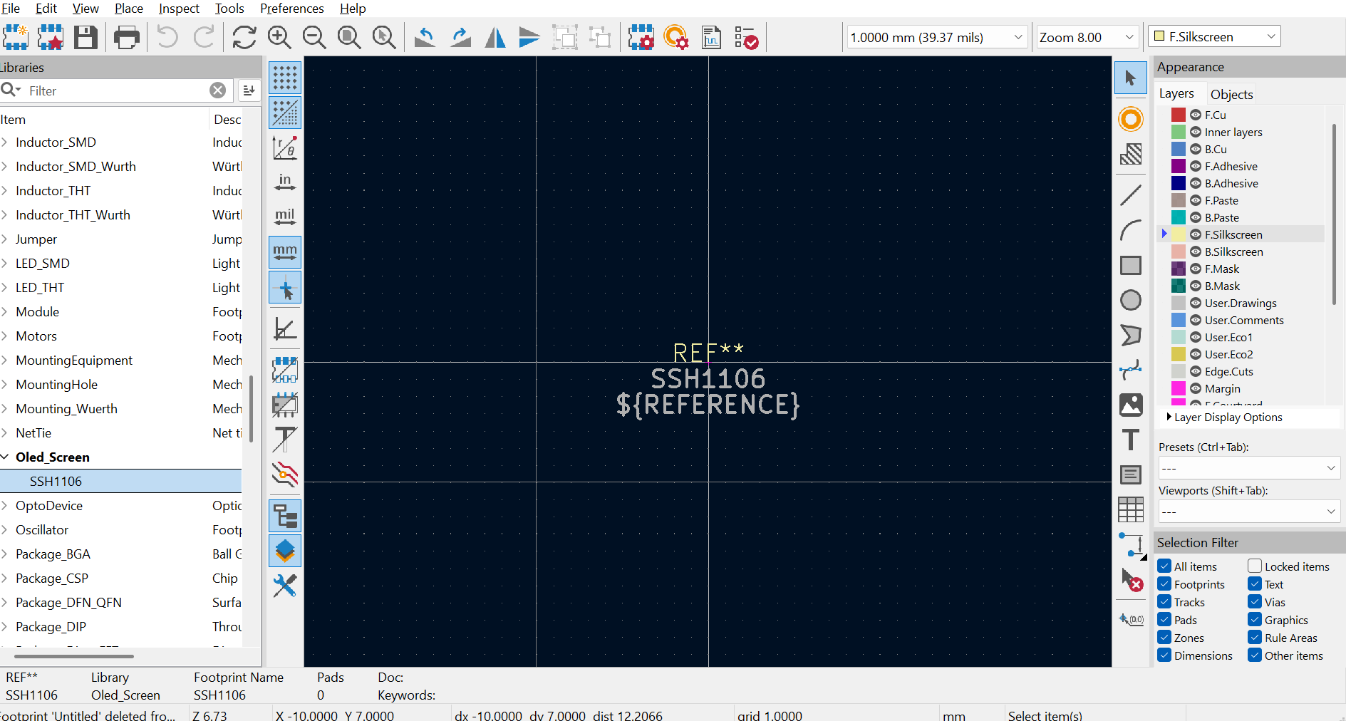
I launched Footprint Editor in KiCad.
I clicked File and New Library.
I again selected Project, and saved a new Library called Oled_Screen.
On the new library, I right clicked it, and chose New Footprint.
I named the new footprint as SSH1106.
On footprint editor, I first changed the division from 1mm to 0.5mm
I then selected draw rectangles.
And, draw one based on my Screen’s dimensions.
After that I dropped my division from 0.5mm to 0.250mm in order to perfectly center the rectangle.
Later, I right clicked on the rectangle.
I clicked on Create From Selection, and then Create Rule Area from Selection.
There, I turn off the Keep Out Tracks and Keep Out Vias. And, I turn on the Keep Out Footprints.
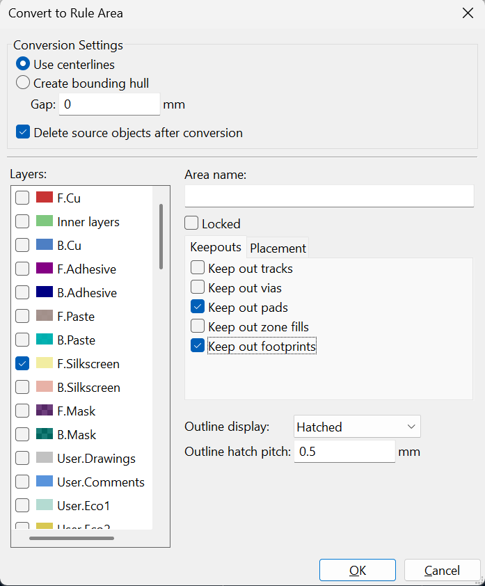
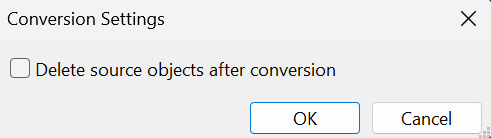
After that, I clicked on Create From Selection, and then Create Lines from Selection.
And, I unchecked that box too.
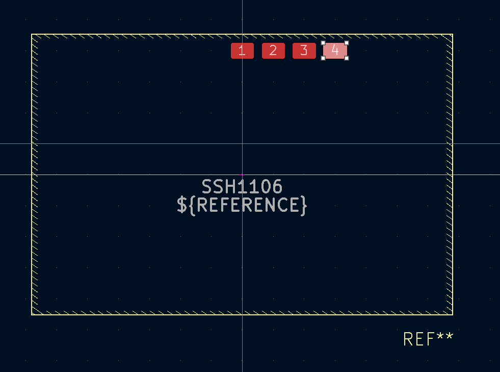
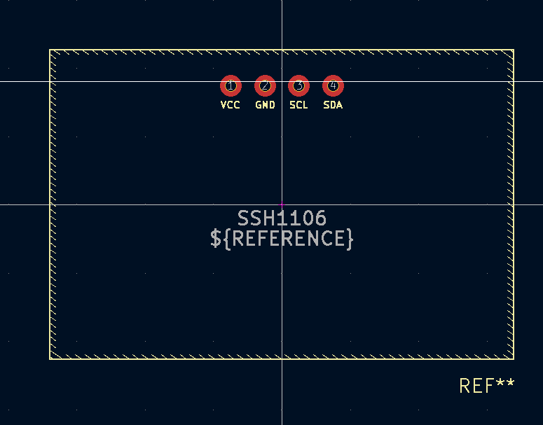
I also pulled the Reference label REF down in the right corner.
I changed my division into 2.5400mm from 0.250mm.
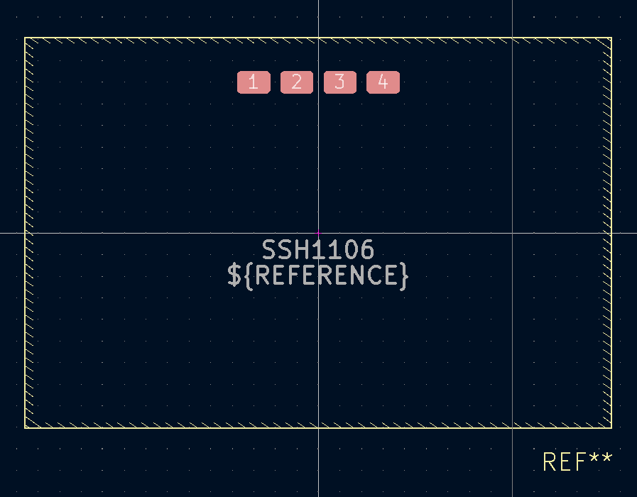
I clicked on Add Pad.
I added pads starting from the center under 1 unit under the top.
I added four pads consequetively.
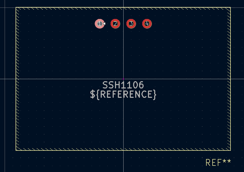
After that, I decreased my divisions from 2.5400mm to 1.2700mm.
I shift clicked at all pads.
Clicked on M button on my keyboard, and moved it to the center of that same position, but just 1 unit under the same position.
I then opened 1st pad’s property.
I changed the Pad Type to Through-hole.
I changed the hole shape diameter from 0mm to 0.762mm.
On right side, I unchecked F.Paste, and checked F.Mask and B.Mask.
I made the Pad Shape Circular, and changed the diameter to 1.524mm.
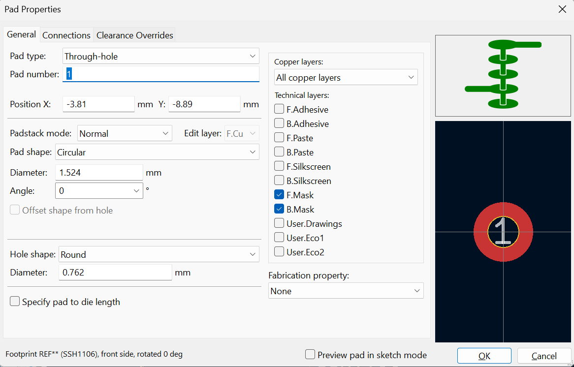
And, I applied this to all of them.
Then, I clicked on Draw Text.
I changed both text width and text height to 0.5mm.
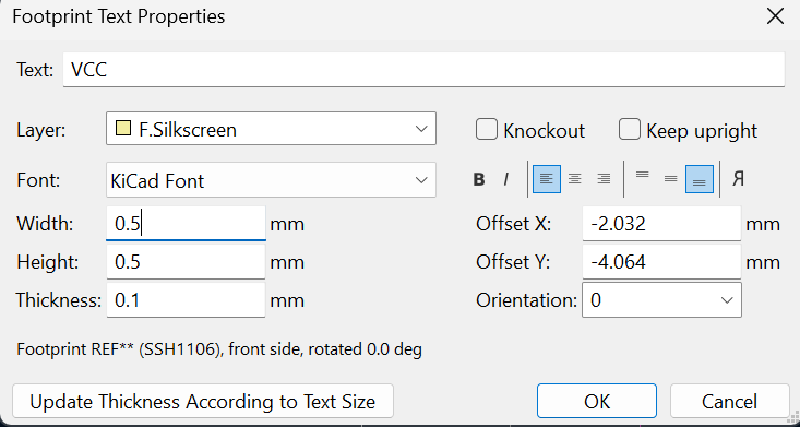
I decreased my divisions to 0.5080mm.
And, I added the actual text labels to all of them, according to my OLED Screen’s layout.
I saved my changes.
I went back to Schematic Editor.
Schematic Editor
Assigning Footprint
I clicked on assign Footprints.
I selected SSH1106.
I found my Oled_Screen foodprint on the left side bar.
I clicked that.
After that, I double clicked to the Oled_Screen on the right side bar at filtered foodprints.
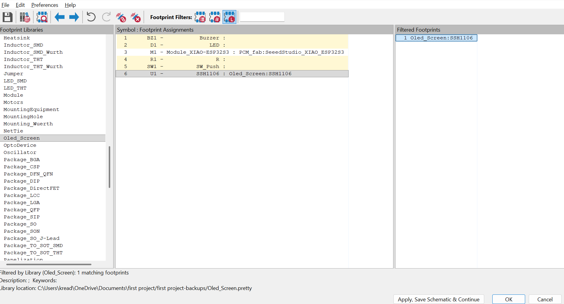
While doing this, I also carefully selected my other footprints that is suitable for what I used.
This take a lot of time because I search one by one on Footprints Editor, and look at the 3d visual of the thing with Alt 3 on KiCad. But, at the same time, it helped me on my BOM List.
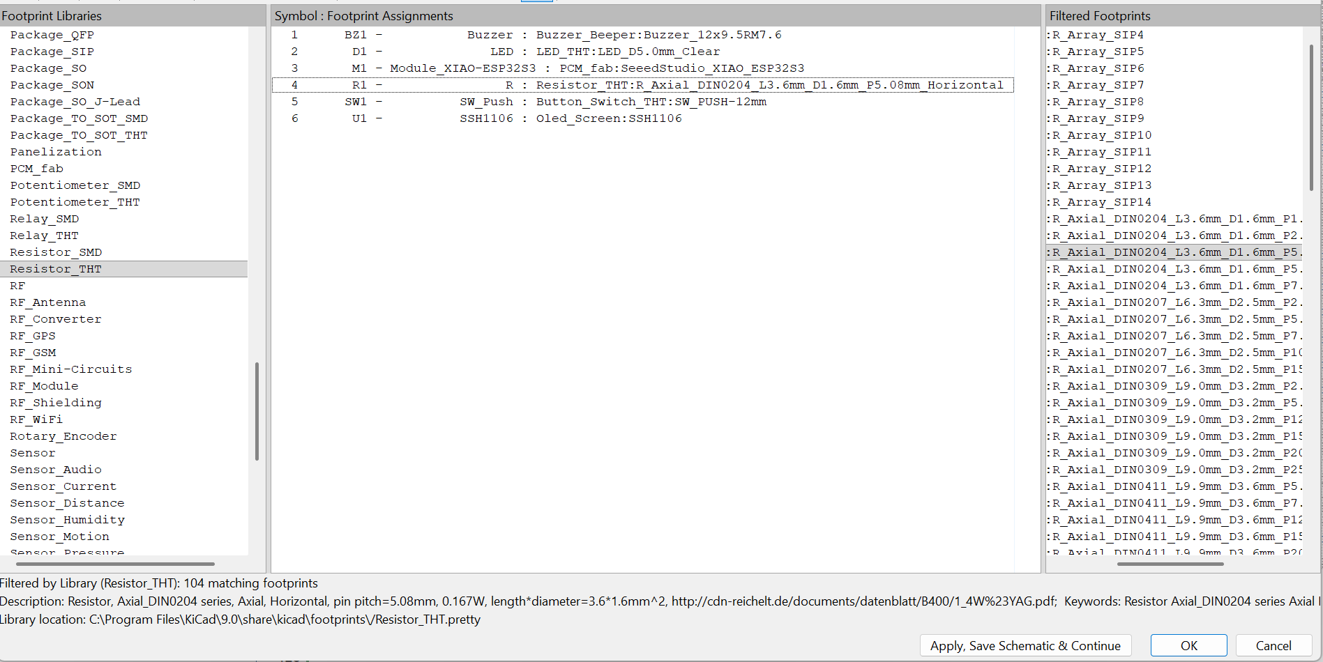
I then clicked OK.
PCB Editor
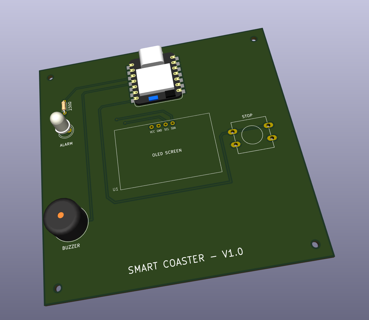
Designing the Board
Here, I started with clicking Update PCB from Schematic.
Use the settings that I used below.
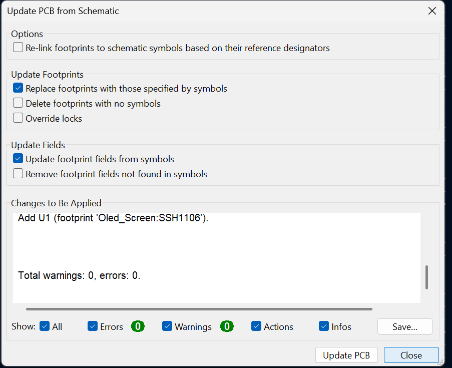
The output will look like below.
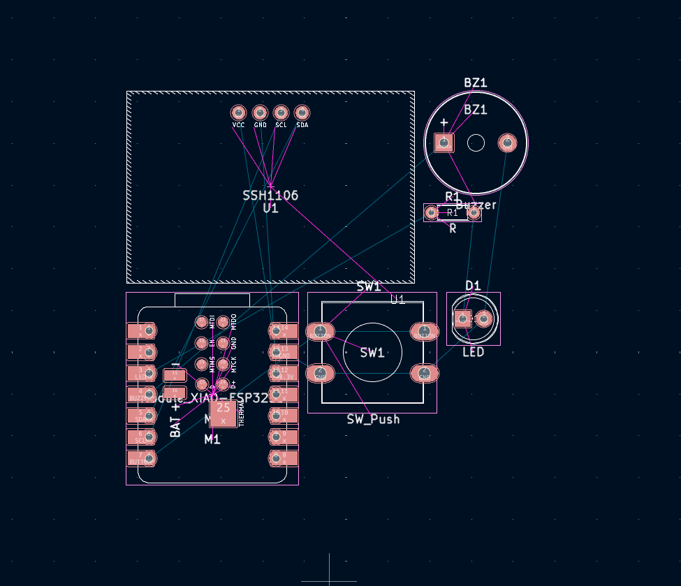
I now imported my design of the final project as DXF from File, Import, and Graphics. This will have locations of the electronic components.
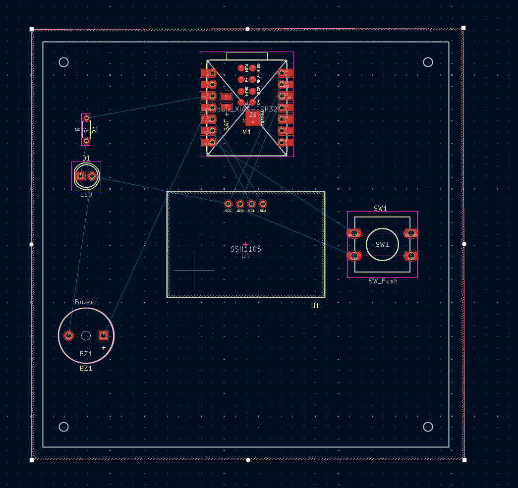
I then clicked on M, and brought each components to their places.
It looked like this at the end.
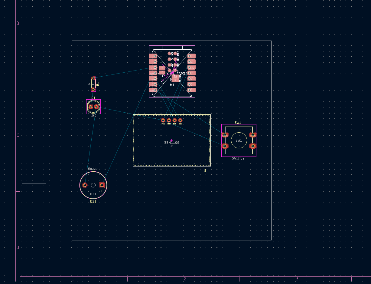
On the right side, I clicked on Edge Cuts, selected my division as 0.2500mm, and Draw Lines around the border of DXF.
I also added mounting hole of the pcb again with Edge Cuts, but on this one, I used Draw Circles.
After that, I clicked on Front Copper Layer on Right Side.
I clicked on the outer side of my board.
I selected GND as net, and I selected Back Copper Layer too at that panel.
I clicked OK, and I draw a square around my board.
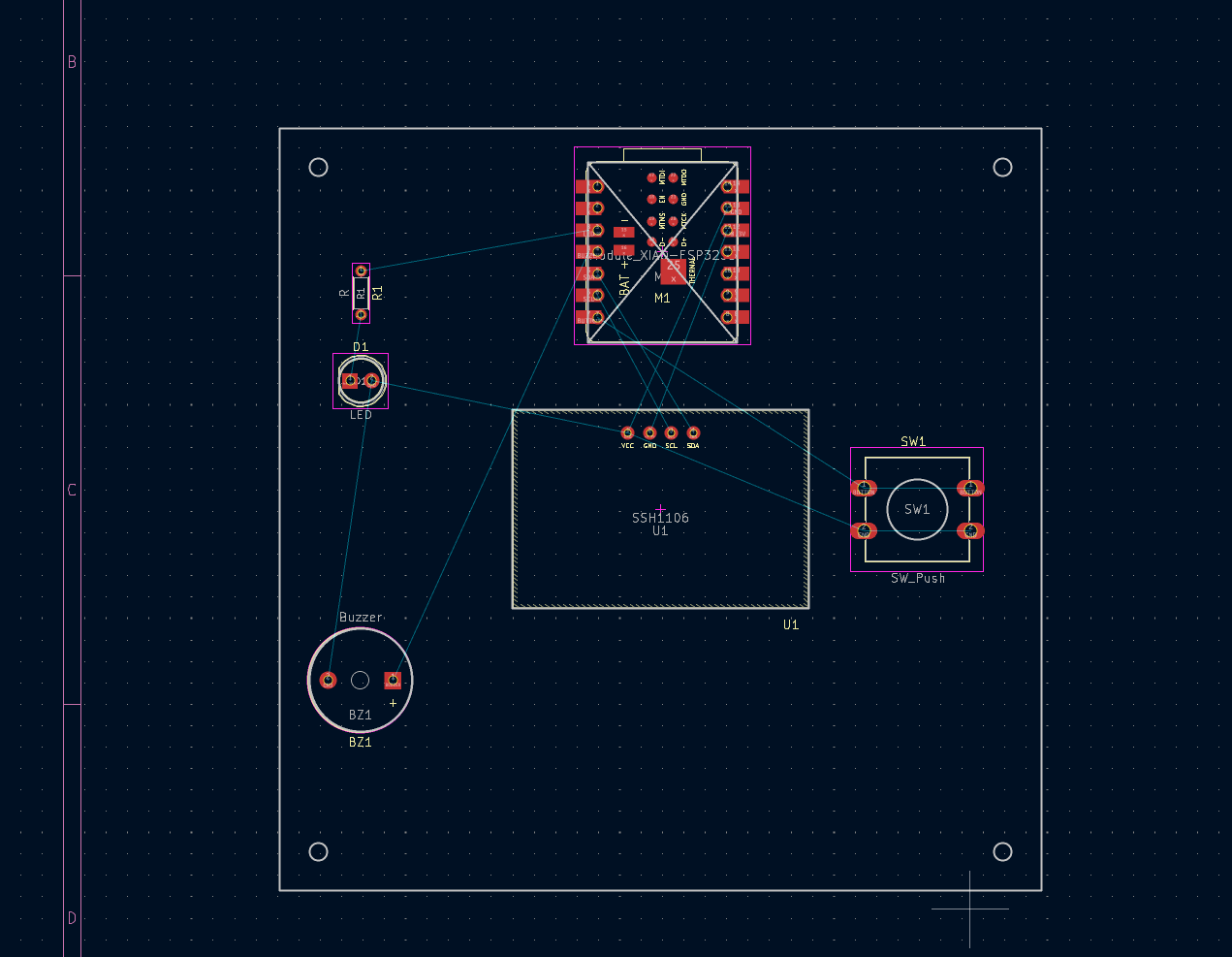
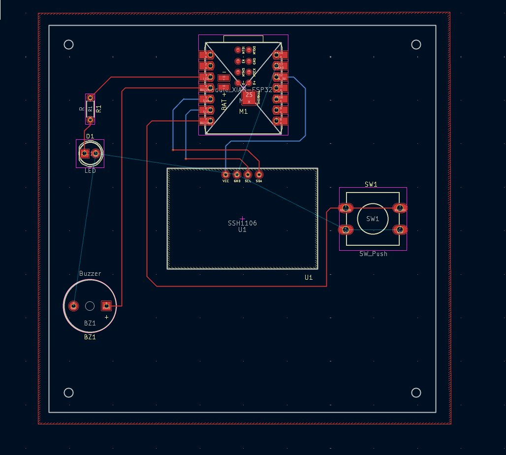
After that, I clicked B on my keyboard.
It changed my GNDs to wire them later on.
And, I started wiring.
For those wires that overlap, I first go with the front red wire, when its near to the overlap I press V on my keyboard, and this make my wire back board, so blue. And, I continue wiring like that.
This is how I wired:
I again clicked B, and Run Design Rules Checker.
There were warnings but no errors.
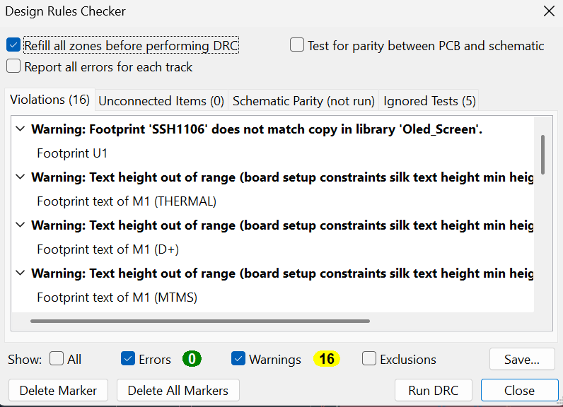
But, the warnings was about the text sizes, so one by one, I clicked properties of each text and changed the text size to 0.6x0.8mm, for the ones that didn’t work.
I finally added some text to my PCB. So, I clicked F.Silkscreen, and Draw Text.
And, I was done.

What I’ve Learned
Learned how to create and manage custom symbols and footprints in KiCad.
Gained experience importing and configuring external libraries for PCB design.
Understood the importance of assigning correct pin types and pin numbers to avoid ERC errors.
Learned how to import DXF files from Fusion 360 and use them as references for component placement.
Improved my PCB routing skills by using both front and back copper layers with vias.
Learned how to align electronic components with a mechanical enclosure design for better integration.
Gained experience using Design Rule Checks (DRC) and Electrical Rule Checks (ERC) to validate a PCB design.
Better understood the complete workflow from schematic design to a manufacturable PCB layout.
Files
You can access to the files of this week from the link below.