Week 6: Electronics Design
Planted February 26, 2026
Overview
This week was a fun week. It was both a chance to explore and contribute to my final project while also getting to design cool and advanced stuff. It started off with the familiar face of KiCad and expanded from there.
Group assignment
Individual assignments
KiCad & Final project boards
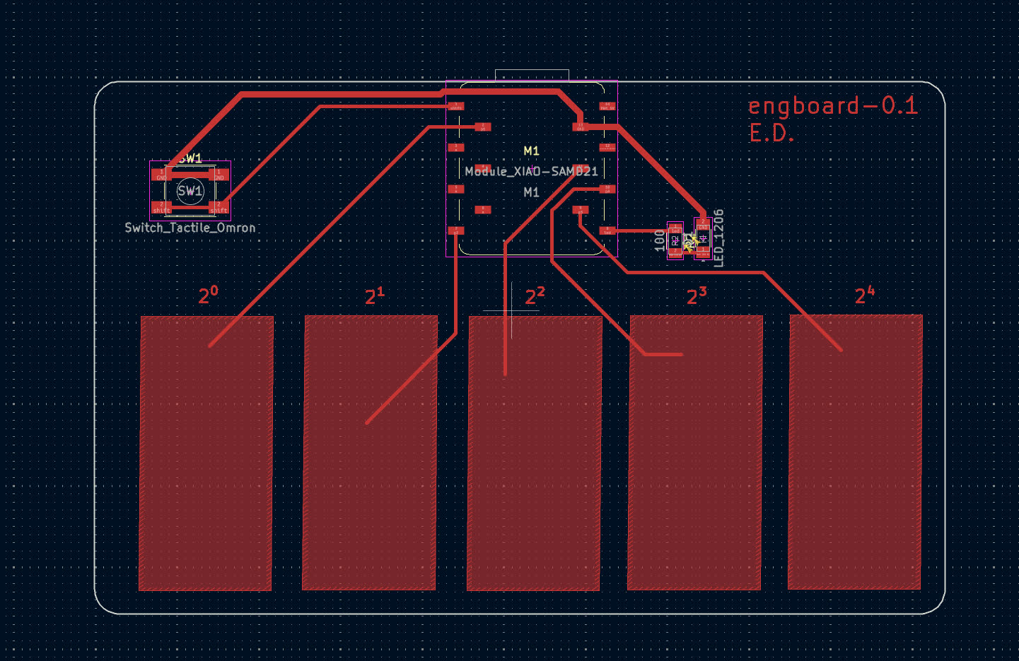
After going thorugh 5 weeks of the course I decided to make a major stride with my final project this week. So I decided to design the sub-module extension boards of the digital productivity device
EngelBoard
I started out with the Douglas Engelbart inspired keyboard. I decided to go with a five capacitive touch pad keyboard where letters are typed based on their place in the alphabet represented by the binary scale. Also I added a tactile button for shift and a LED for status. Below is the schematic

After finishing the schematic to make sure everything was electrically sound I ran an ERC (Electrical Rule Check). ERC validates the schematic, unconnected pins, conflicting outputs, power issues, and similar, so the circuit is logically and electrically consistent before moving to layout.

Then I started routing the PCB, but before that I had to make some changes in the netlist to have a better routed board. I changed the default track width and clearance accordingly to 0.4 mm’s to reduce the resistance in the tracks to have better passing of signals.

additionally since I had pads, I couldn’t make the whole circuit board the ground hence, I had to make the grounds thicker to ensure safety of the board, I did that as below

Below is the final result post routing

After finishing the routing I ran a DRC (Design Rule Check). DRC validates the PCB layout against the design rules—clearances, track widths, pad sizes—so the board can be manufactured without shorts or other fabrication issues.

iSynth
The next module was a snyth. It’ll be both be able to be ran by a buzzer or connected to the main device to save created beats to later listen to. For this I needed more gpio’s so I used the ATSAMD21E17A. Along side this 8 capacitive touch pads for various functions, 5 being used for the Pentatonic Scale, a buzzer, a ws2812b RGB led as a physical response when pads are clicked, to tactile buttons to change octave and record respectively. Also it has a 4 pin SWD to programm and a usb port for connection.

Then I routed the board and got a result as below

Once again I ran the ERC and DRC tests for the sch and the pcb respectively and once again no such errors popped up.
Experimenting
Verilog
4-bit ALU in Verilog with 16 operations, inspired by the 74181. The ALU is combinational logic: two 4-bit operands (a, b), a 4-bit operation select, and a 4-bit result plus five status flags. Synthesized with Yosys; testbench runs 500 random tests.
Ports: Inputs: a[3:0], b[3:0], select[3:0]. Outputs: out[3:0], zero, carry, sign, parity, overflow. The flags are computed after every operation: zero = result is all zeros (NOR reduction); carry = carry/borrow out of the MSB for arithmetic; sign = MSB of result (negative in two’s complement); parity = even parity of result (XNOR reduction); overflow = signed overflow for add/sub/inc/dec.
Operation table (from alu.v):
| Select | Operation | Description |
|---|---|---|
| 0000 | ADD | a + b with carry and overflow |
| 0001 | SUB | a - b with borrow and overflow |
| 0010 | MUL | a * b (5-bit result; carry holds upper bits) |
| 0011 | DIV | a / b, returns 0 on divide-by-zero |
| 0100 | AND | Bitwise AND |
| 0101 | OR | Bitwise OR |
| 0110 | XOR | Bitwise XOR |
| 0111 | NOT | Bitwise NOT of a |
| 1000 | SHL | Shift a left by b; shifted-out bit in carry |
| 1001 | SHR | Shift a right by b |
| 1010 | ROTL | Rotate a left by b (wrap) |
| 1011 | ROTR | Rotate a right by b (wrap) |
| 1100 | GT | 1 if a > b, else 0 |
| 1101 | EQ | 1 if a == b, else 0 |
| 1110 | INC | a + 1 |
| 1111 | DEC | a - 1 |
Design notes: Sensitivity list is always @ (a or b or select) so the block recomputes on any input change. Add/sub/inc/dec set overflow when the signed result would not fit in 4 bits. Shift left uses {carry, out} = a << b; rotate uses (a << b) | (a >> (4 - b)) for left and the reverse for right. Divide guards against divide-by-zero with b ? a / b : 0.
Process: The RTL is in alu.v; the testbench (alu_tb.v) drives random a, b, and select, computes the expected result for each op, and compares to the ALU output. Run iverilog -o alu_test alu.v alu_tb.v && vvp alu_test for 500 random cases. Yosys reads the Verilog, runs proc and opt, then outputs gate-level netlist (synth.v) and the circuit diagram.
iverilog -o alu_test alu.v alu_tb.v && vvp alu_test

Files in verilog/: alu.v, alu_tb.v, synth.ys, view_circuit.sh, synth.v, circuit_diagram.jpg.
PCB.py
I came across Quentin Bolsee’s talk on F-Rep (function representation) PCB parsers and built a multicore CPU version. F-Rep models geometry with math functions instead of polygons, enabling parametric PCB designs. The solver reads PCB.py’s JSON from stdin, evaluates over a 2D grid (one or more Z layers), and writes an RGB PNG—NumPy+PIL by default (100 DPI) or optional C backend (--c, 300 DPI) with pthreads for speed.
How it works: The JSON carries a single math expression (e.g. a circle or PCB shape). The solver samples that expression at every (x, y) on a grid for each Z layer; where the expression is true the pixel is set, otherwise it stays background. Where multicore comes in: the grid has many thousands of points, so the work is embarrassingly parallel—each CPU core gets a band of rows, evaluates the expression only for those (x, y), and writes into a shared pixel buffer; no cross-core dependencies, so you get a near-linear speedup with core count. Two backends: NumPy uses multiple cores internally for the array math (portable); the C backend spawns one pthread per core, each handling its row band, then exports PNG with correct DPI.
Key parser snippets:
- Expression conversion (Python → C):
def python_expr_to_c(fn):
    fn = fn.replace('X', 'x').replace('Y', 'y').replace('Z', 'z')
    fn = fn.replace('math.', '')
    fn = re.sub(r"\bpi\b", 'M_PI', fn)
    while '**' in fn:
        fn = re.sub(r"(\S+)\s*\*\*\s*(\d+\.?\d*|\w+(?:\.\w+)?)", r'pow(\1,\2)', fn, count=1)
    fn = fn.replace(' & ', ' && ')
    fn = fn.replace(' | ', ' || ')
    fn = fn.replace('~', '!')
    return fn
This lets the same F-Rep expression string run in both Python (NumPy) and in generated C without changing the original JSON.
- NumPy grid evaluation and layering:
x = arange(xmin, xmax, delta)
y = flip(arange(ymin, ymax, delta), 0)
X = outer(ones(y.size), x)
Y = outer(y, ones(x.size))

if len(frep['layers']) == 1:
    Z = frep['layers'][0]
    f = eval(frep['function']).astype(uint32)
else:
    f = zeros((y.size, x.size), dtype=uint32)
    zmin, zmax = min(frep['layers']), max(frep['layers'])
    for Z in frep['layers']:
        i = int(255 * (Z - zmin) / (zmax - zmin)) | (255 << 8) | (255 << 16)
        flayer = i & (eval(frep['function'])).astype(uint32)
        f = f + flayer
Here NumPy builds the X/Y grids and evaluates the F-Rep function over them; each Z layer is encoded as a different color/intensity and accumulated into one RGB image. The C backend mirrors this logic but splits rows across threads.
Usage:
pcb.py | frep_multicore.py [dpi [filename]]
pcb.py | frep_multicore.py --c [dpi [filename]]
python3 basic.py | python3 frep_multicore.py 1000 sample_design.png

Output matched the same render test as the GPU version. Source: frep_multicore.py
Design
How you design in FRep: Instead of drawing polygons or traces, you describe the board as a single math expression in (X, Y) and optionally Z (for layers). For example a circle is “inside if distance from center < radius”; pads and outlines are built from primitives (circles, rectangles) combined with min/max or logical ops. You write that expression (e.g. in Python) and export JSON; the solver then rasterizes it to a PNG. So design is parametric—change a variable and the whole shape updates.
The designing with the frep is currently being finalized the current status is as below.

SVG-PCB
This was a tool I was excited to try. As one that has cited it’s paper and drawn inspiration from it SVG-PCB is a tool which I am excited to use. I went first to the learn section to choose a board to remix

I stumbled upon the ATTiny412 servo board an decided it was the one to run this little experiment

I decided to add an i2c board so I used the already avaliable component library to import the i2c template. Then looking at the ATTiny412 pin out diagram found the i2c pins, PA1-SDA- and PA2-SCL- and then through the correct routing completed the board as below

short feedback: the wiring on the canvas was at first hard to get, but after some make, fail, learn, repeat.) I was able to get it