Week 8 - Electronics Production
The Electronics Production
Default settings.
Make the PDF .svg.
 First adjustments with “Inkscape”
Changed it.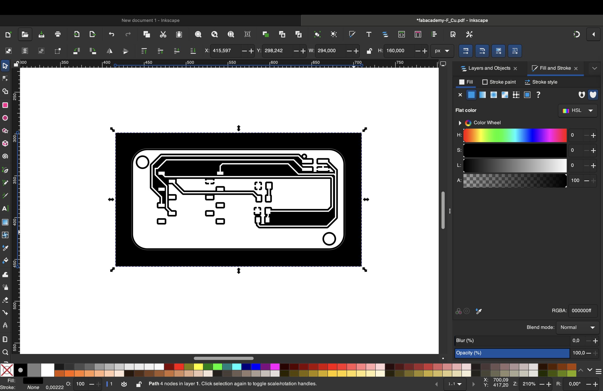 After all the mistakes, I started over. Firstly, I changed the default settings
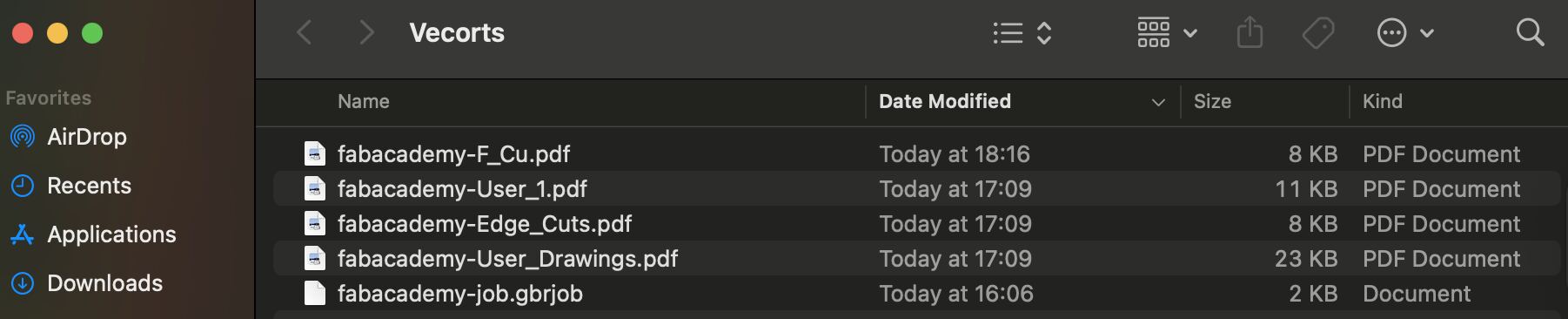
And as you can see at the top, there is a file named “Vectors” that the system automatically added to the “Vectors” file that I created, and this is how the file looked after the process.
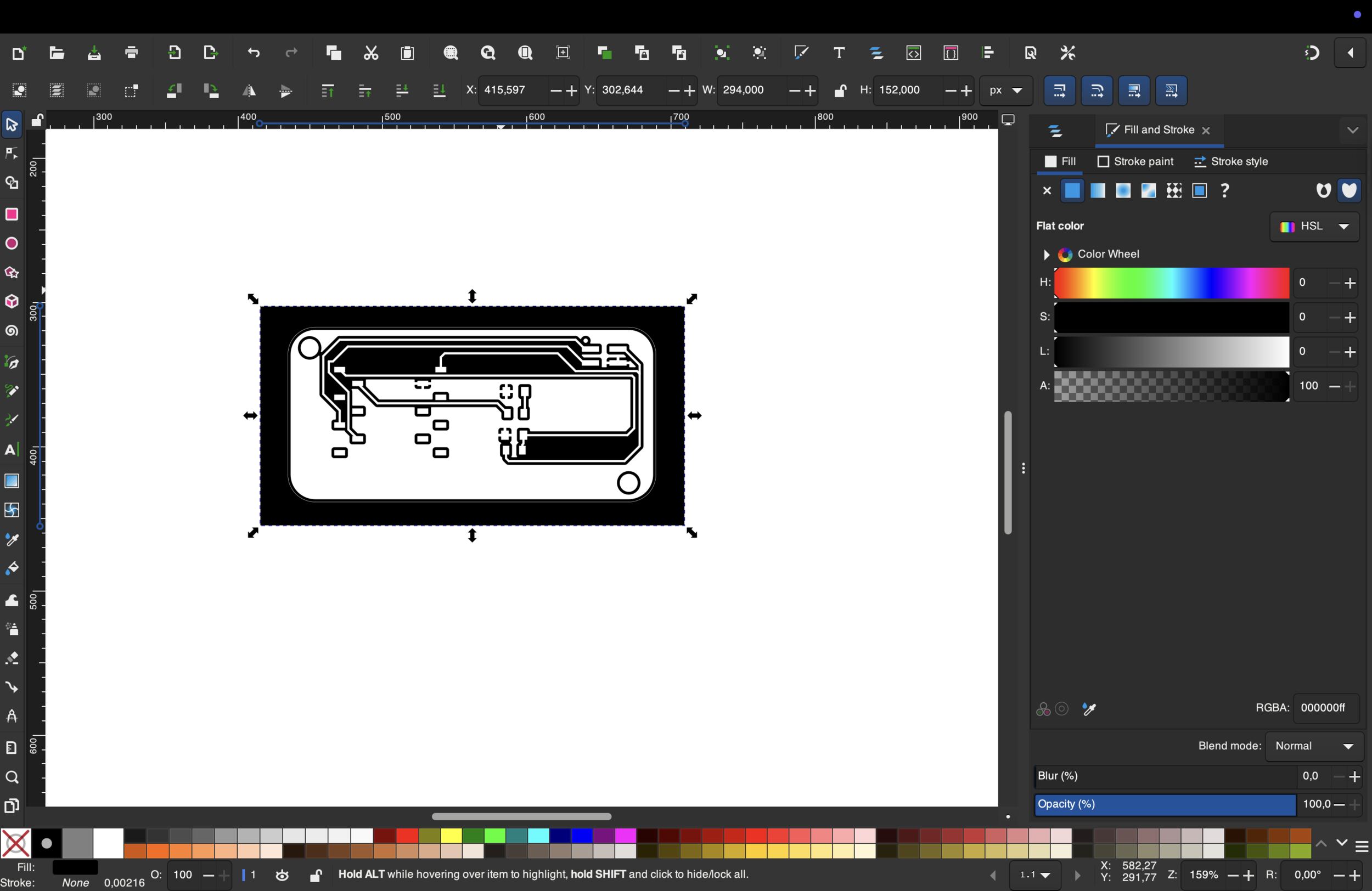
Now we have to turn our PDF files into .svg and we do it with the help of “Inkscape”. We use Inkscape to remove unnecessary space in the background and make the color of the drawings, holes, and text black. I used this button to remove unnecessary space.

And when all the processes come to an end, here is my final designs that I made in “Inkscape”.


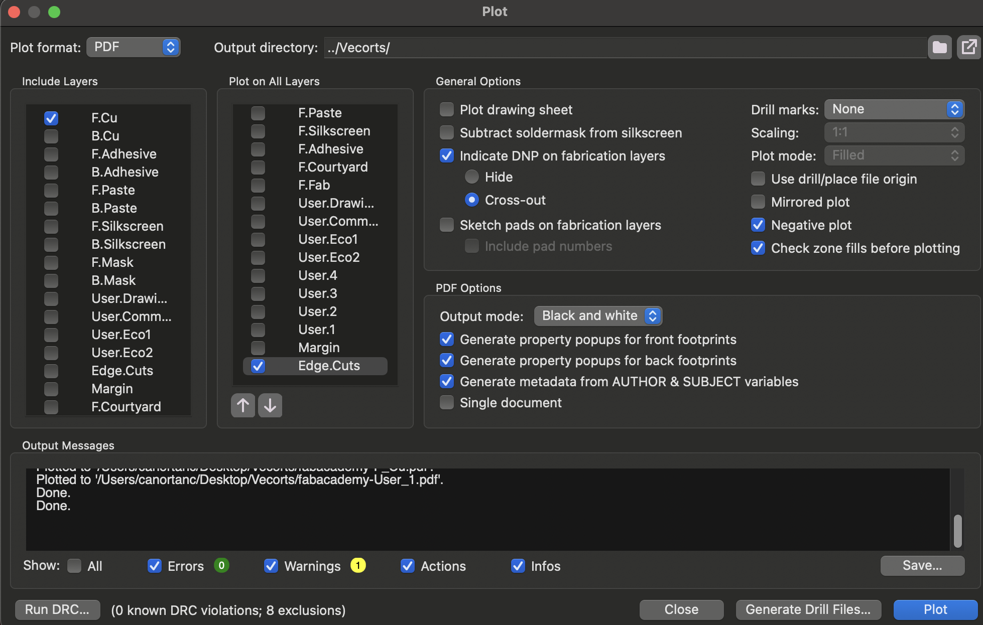
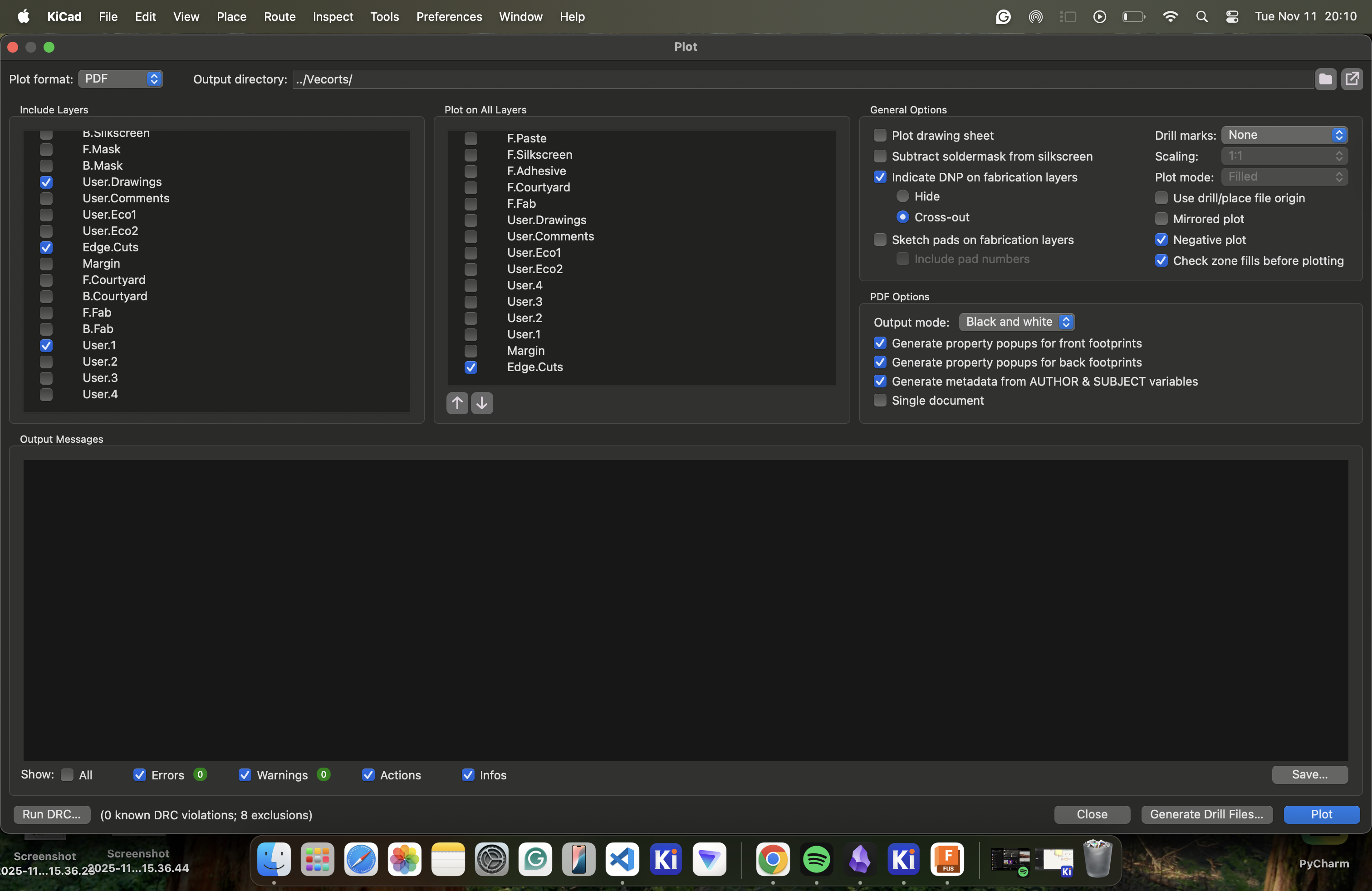
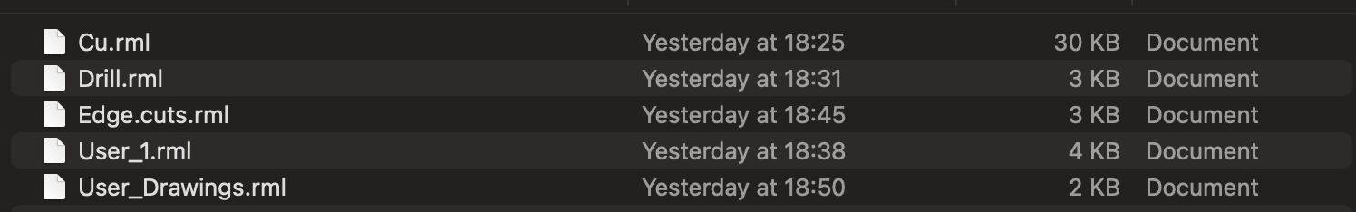
When I finished converting the PDF to .svg I had to change this .svg to rml, and I used the “https://modsproject.org/" website and the settings Mr. Kris gave us at the afternoon lecture but there was a little part Mr. Kris didn’t showed us but cost some errors when doing the drilling and engraving we should have changed x, y and z cordinates to 0, make jog height 3 mm and changeg offset number 4 to 1 because of that mistakes at my first files i started over and here is my first files:
For the setting, firstly, you should right-click the board and choose “programs” and “open program”. It should look like this after the 2 steps.
When the program menu opens, the “mill 2D PCB” in the “SRM-20 mill” should be selected and something like this should pop up.
And like I showed in the video, we put our svg. files we want to get converted to the “select SVG file” part, which is in the very left rectangle, where we decide the input to the program.
I used a specific part to separate parts, for example, we have 2 actions in the system: 1 drilling and 1 engraving. In the engraving part, we do the F_Cu, User_1, and User_Drawings. In the drilling part, we do the Holes and Edge_Cuts. Like I said, Mr. Kris used special settings for both of these processes, and in the drilling part, the settings are like this. The reason was that we used both different drills and I looked up the depth of them from this link that our TA Ömer told me https://www.bungard.de/en/consumables/consumables/drills-and-routers:
For Edge_Cuts and Holes :
For F_Cu, User_1, and User_Drawings :
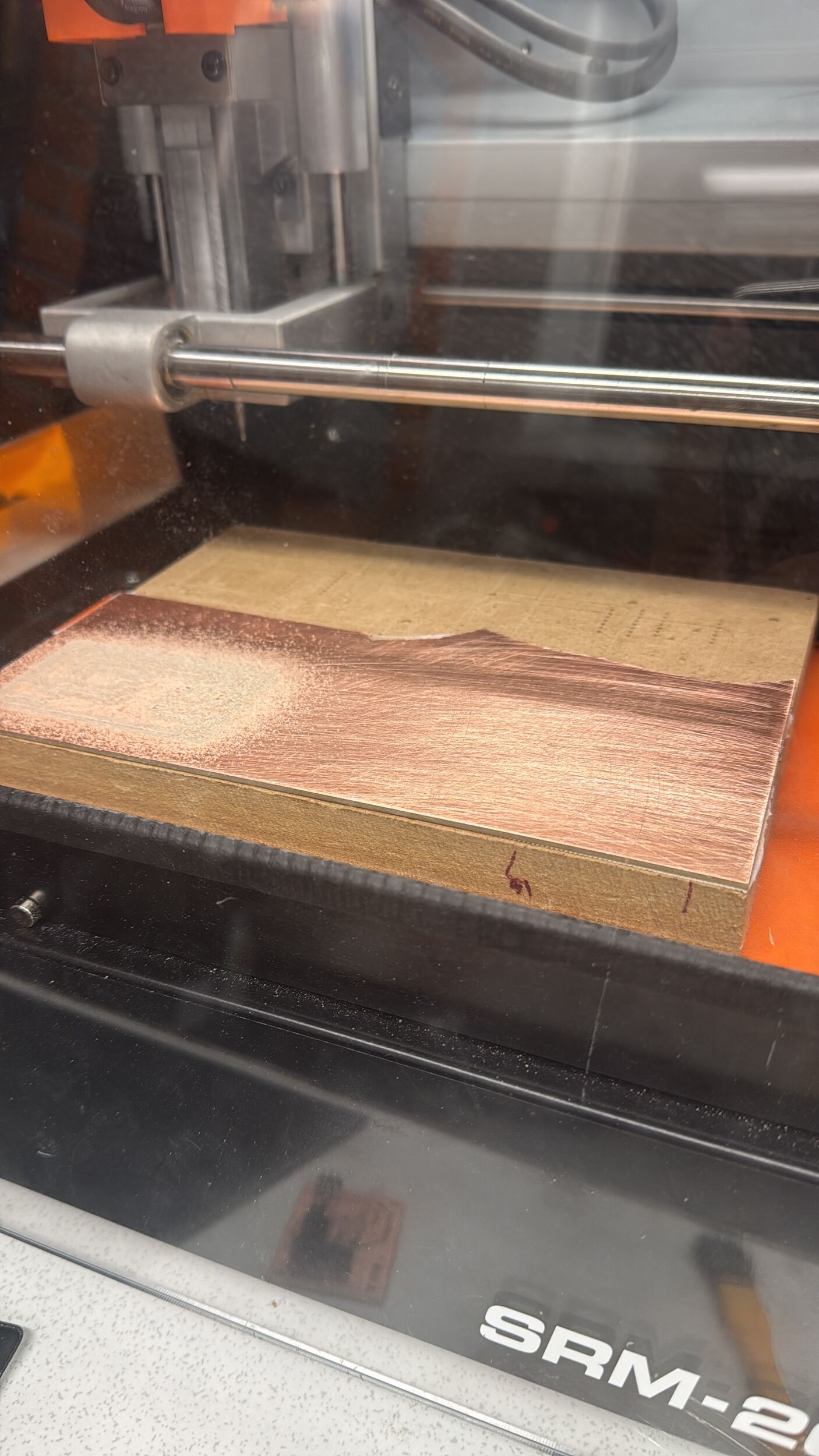
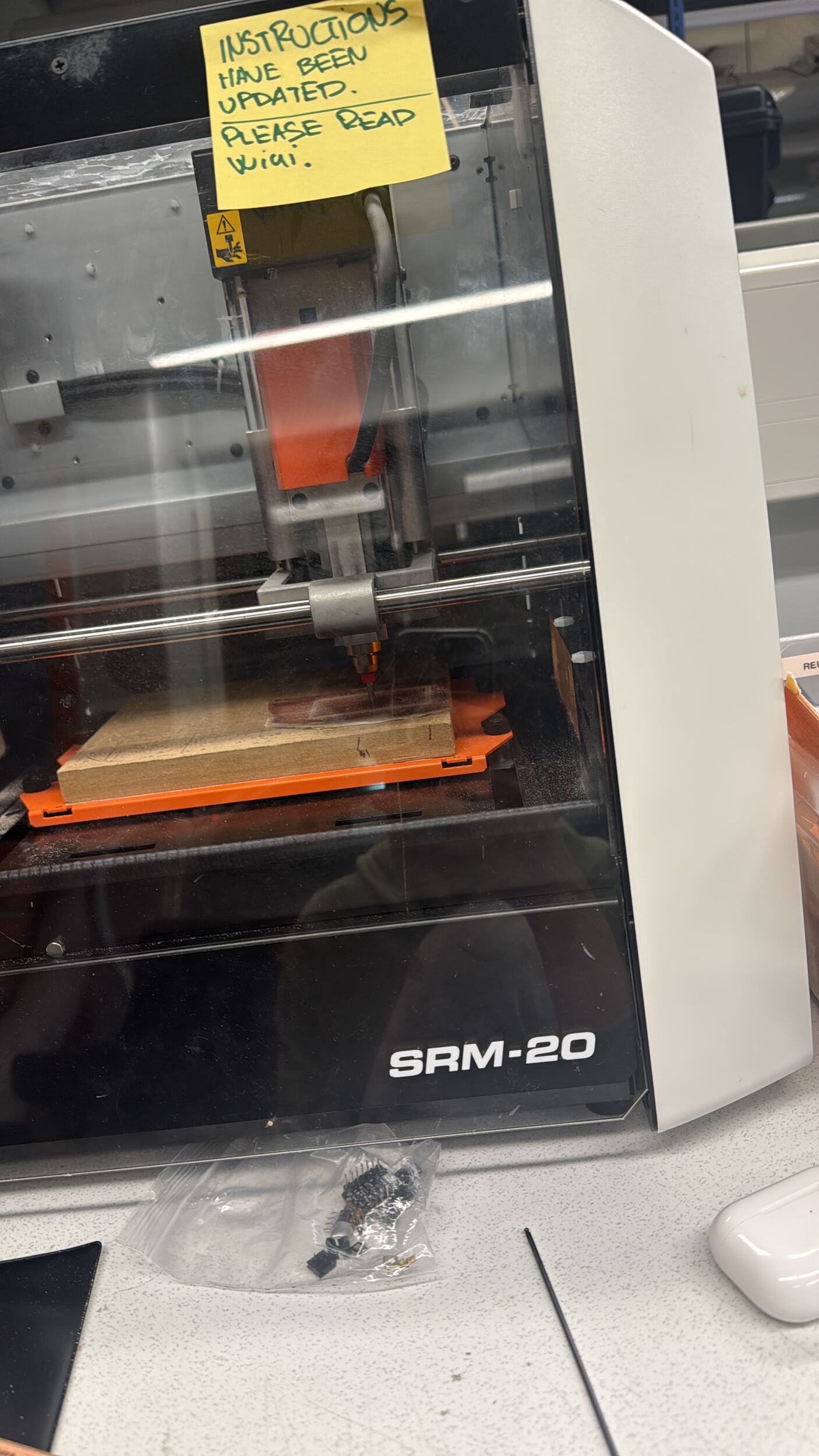
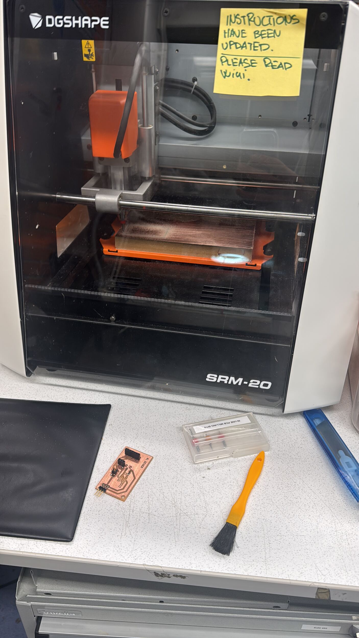
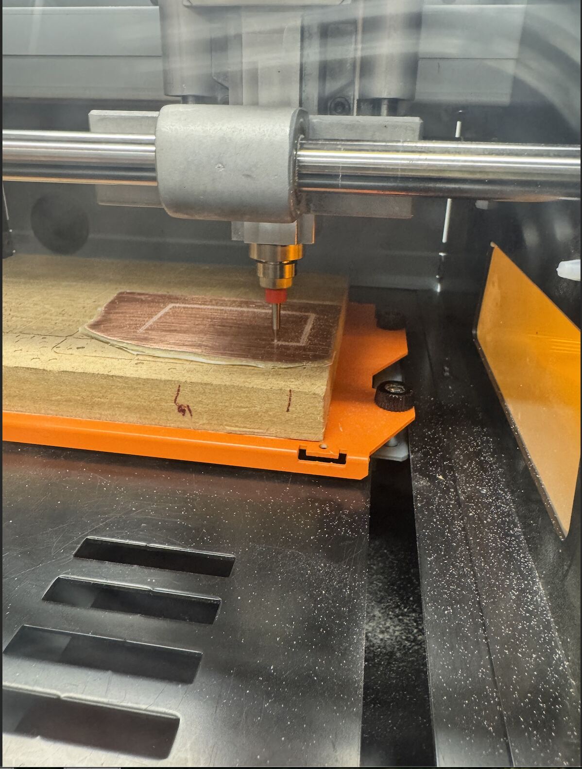
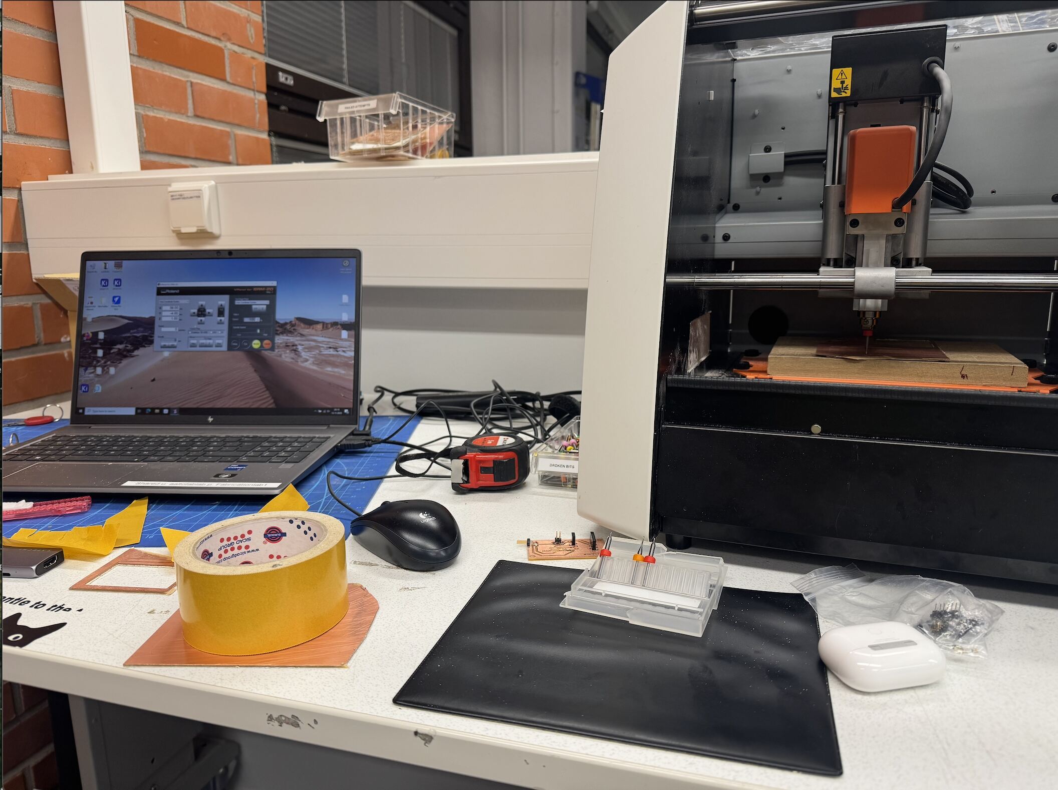
This is what I did for all my .rmls. After that, I directly got these .rmls on a flash disc and put it into the main computer, where we are going to process the engraving and drilling part that happened with the help of my TA Ömer, and here are some clips and photos from it :)
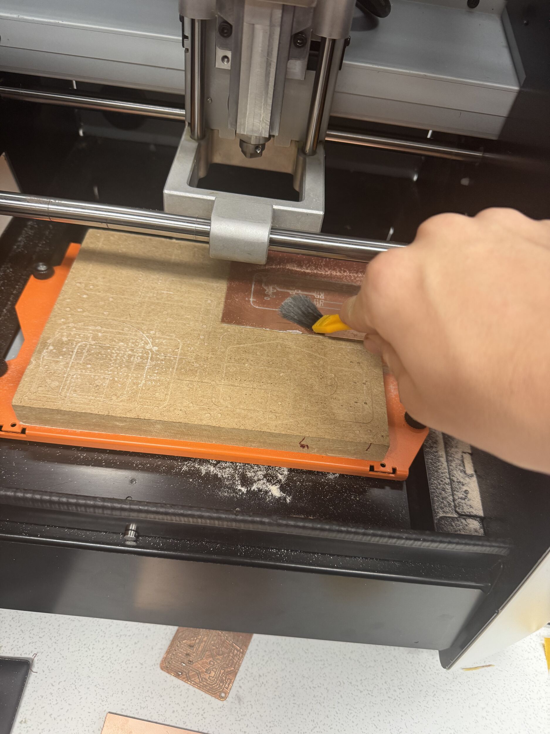
This is the process:
This is me cleaning the board:
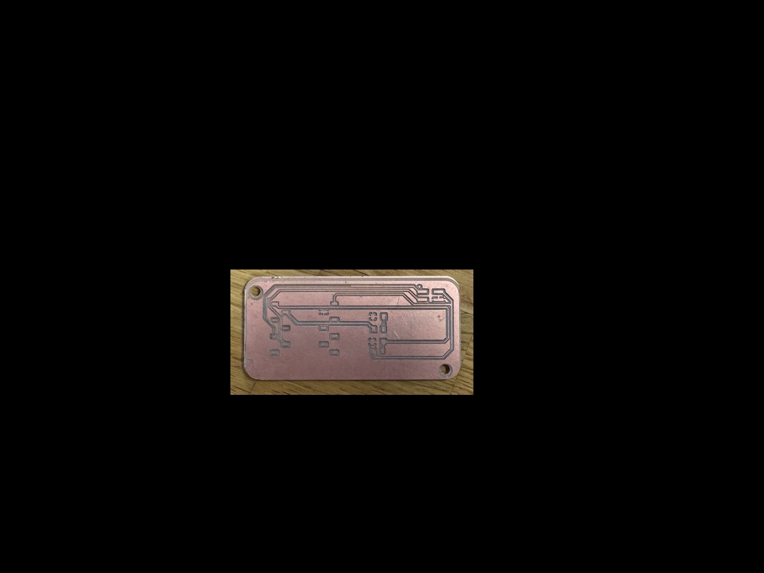
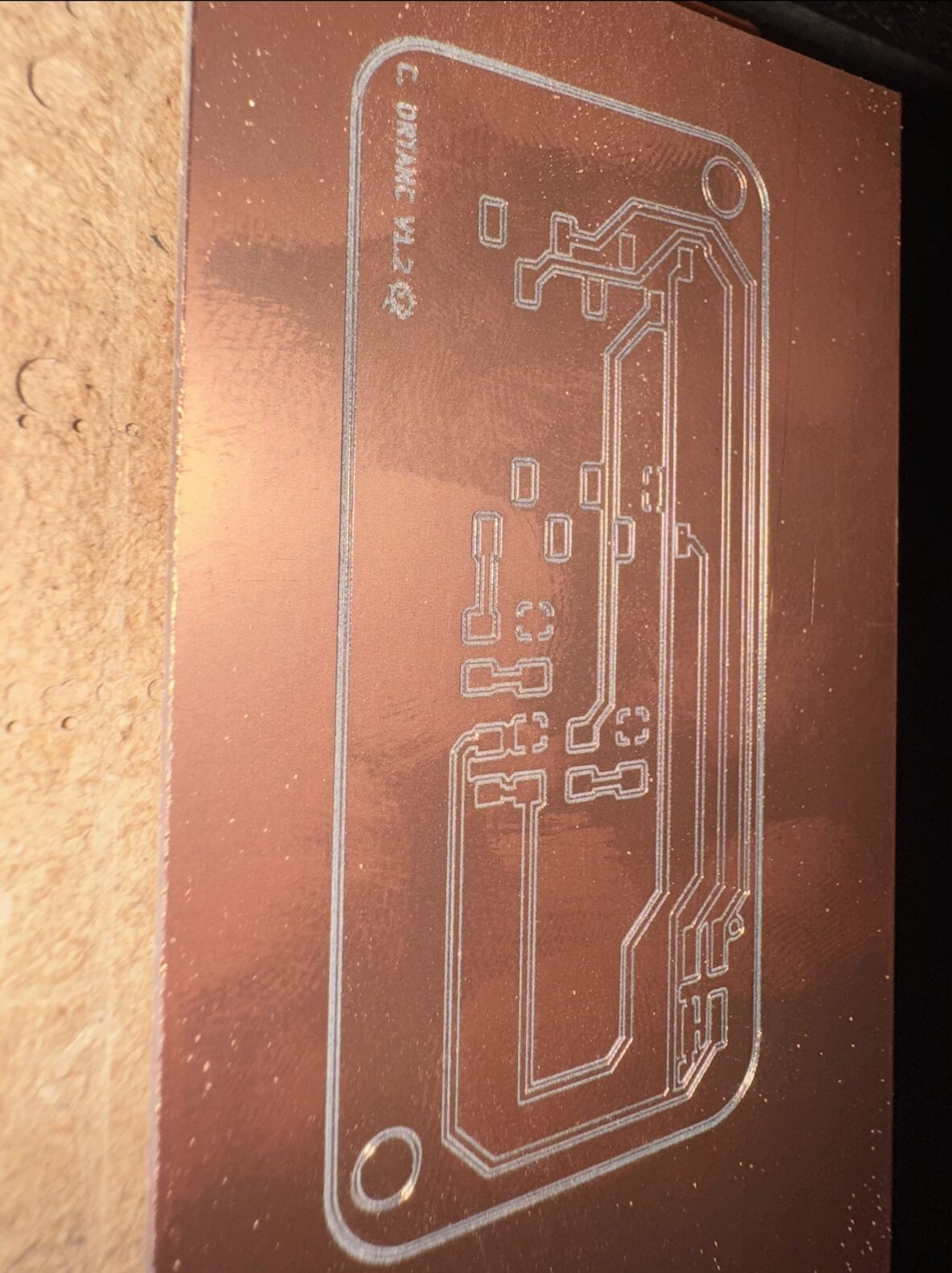
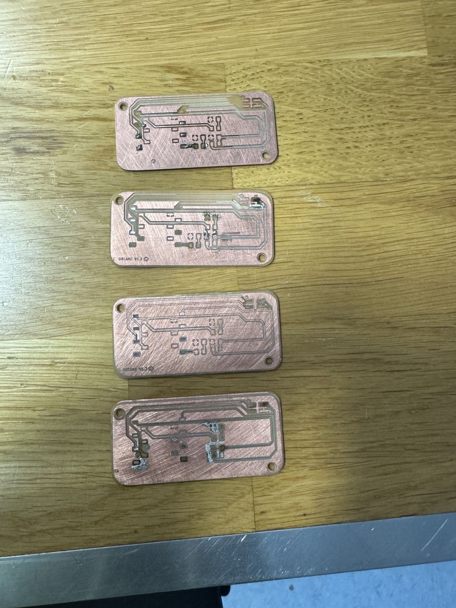
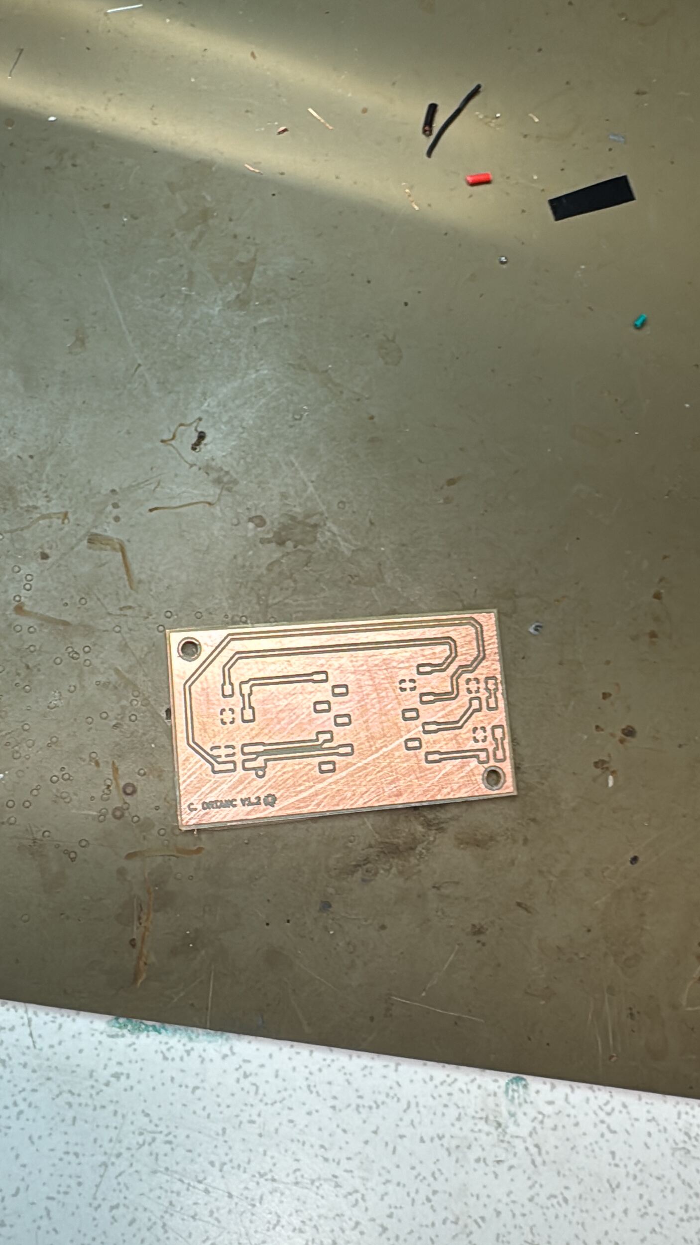
This is the aftermath of the whole process (The whole PBD):
 You can think that this is fine and i thinked that this was fine until i see 3 odd things.
First :
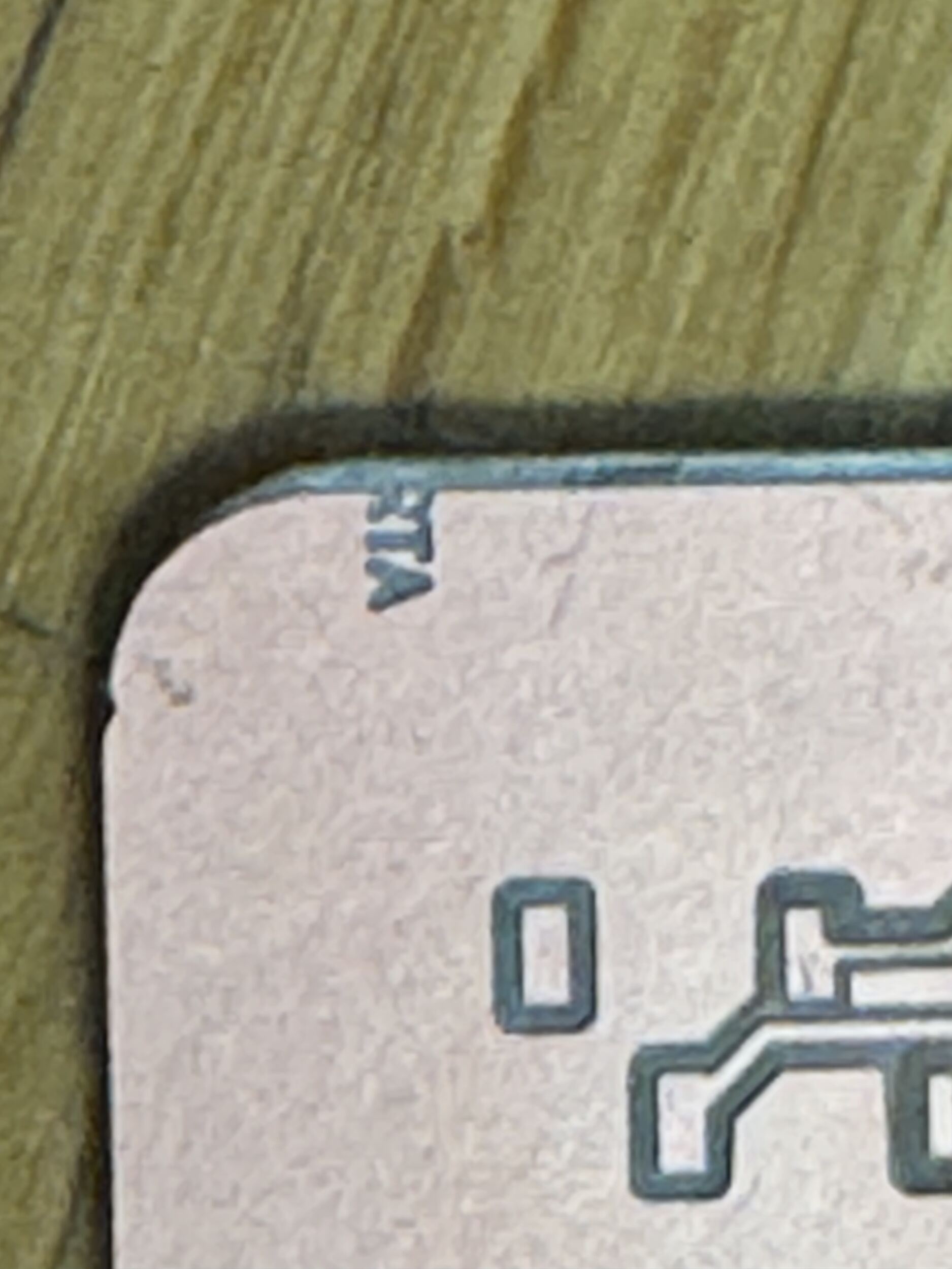 My name, surname, and model v 1.2 are not engraved and are gone from half
Second :
This can be seen from this photo that the guy who is hiding behind the copper escaped like he was not engraved, and I couldn’t bring him back :((((.
Third :
 You see the big line that should be cut, but because I messed up the Edge_Cuts and the User_1 (my name) at the very beginning in InkSpace, this happened.
But these 3 odd things that are considered a failure to me don’t block the PCB from working, and here is the proof of it.
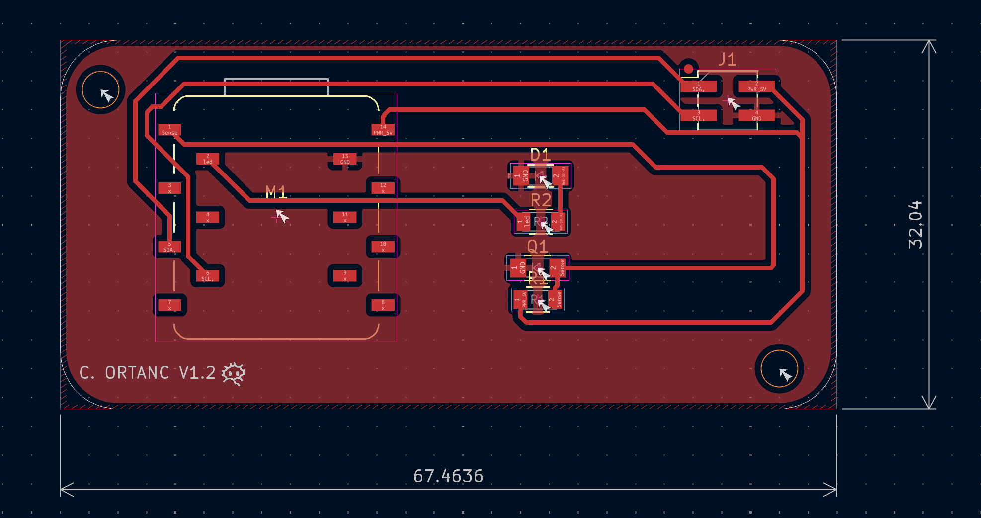
You see, I tested it knowing that there is an electrical connection between every square part in the PCB, but that doesn’t mean I am fine with a working PCB with no design. Because of that, I readied all documents today for tomorrow to make my second PCB board. And after all that, Mr. Sedat gave me a reflection about increasing the distance between lines, and I did it because his reflection is so valuable to me. Here are the new PCB, InkSpace designs, and new and old .rml files.
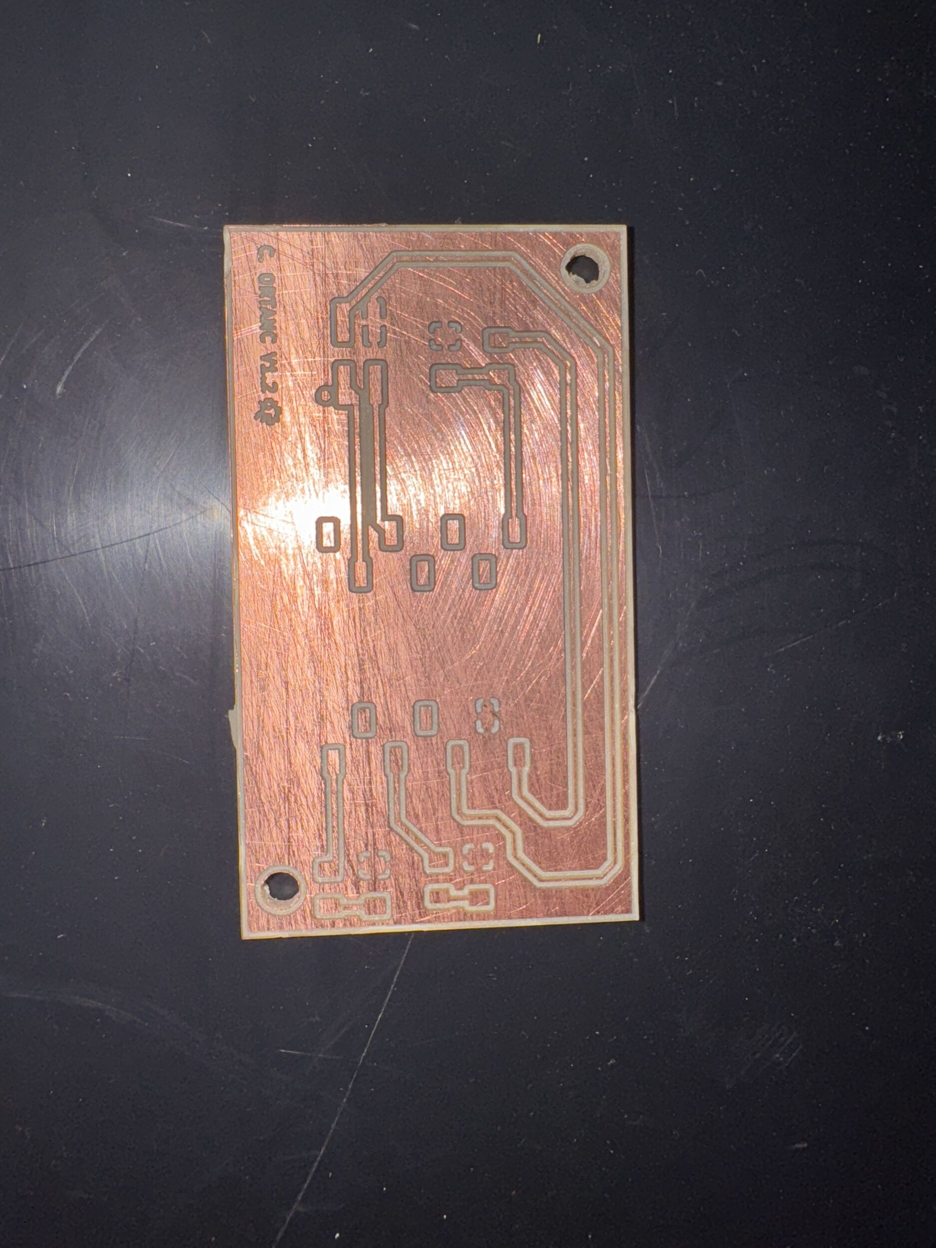
PCB:
InkSpace:


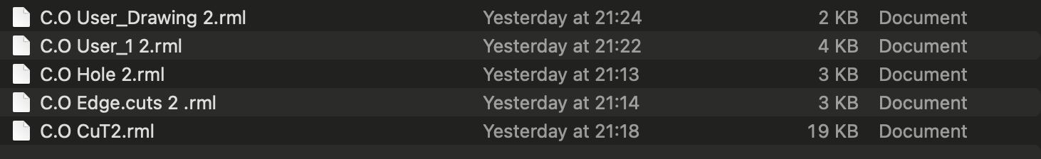
Old .rmls :
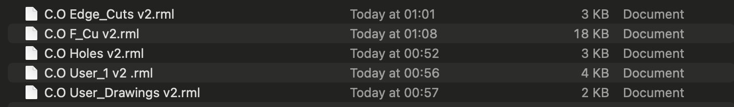
New .rmls :
In all these new files, according to my calculations and the lecture Kris has taught us, everything is going to be perfect with my PCB being perfect.
“A working product with no design is a normal product. But a working product with a design is A PRODUCT”
After all that i learned
I learned about Engraving / Isolation / Drilling parts with 2 types to do it: “V-Bit 60 °” and “V-Bit 90 °.”
Learned how to decide tip diameter, cut, and depth according to “V-Bit 60 °” calculations in mods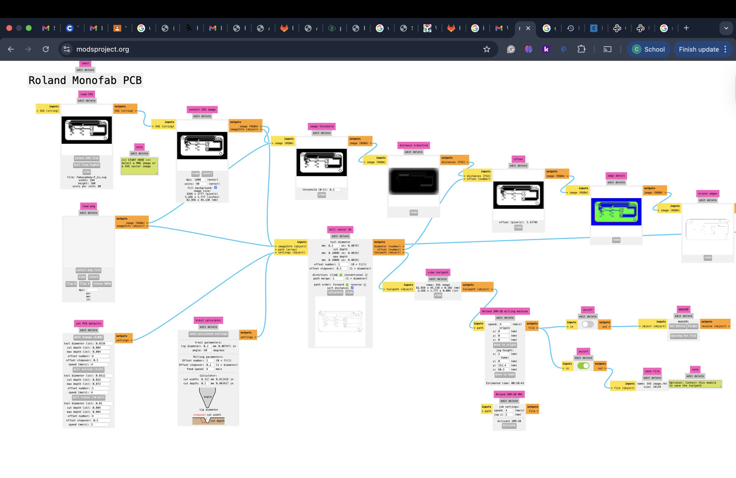
Using trigonometric and tan formulas to calculate the trace (cut width) manually. And talked about our engraving parts products of usage.
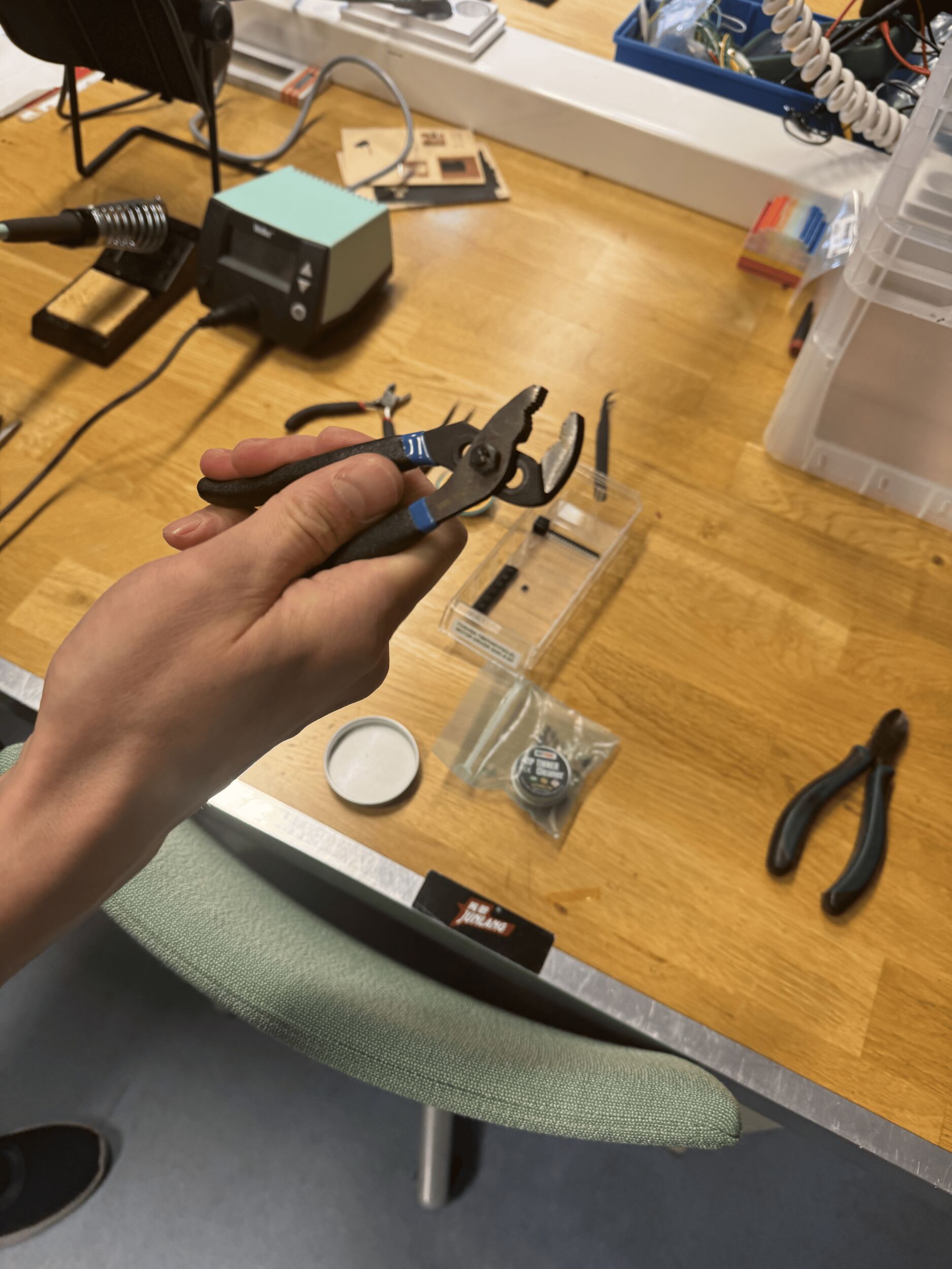
Here is the box and tools:
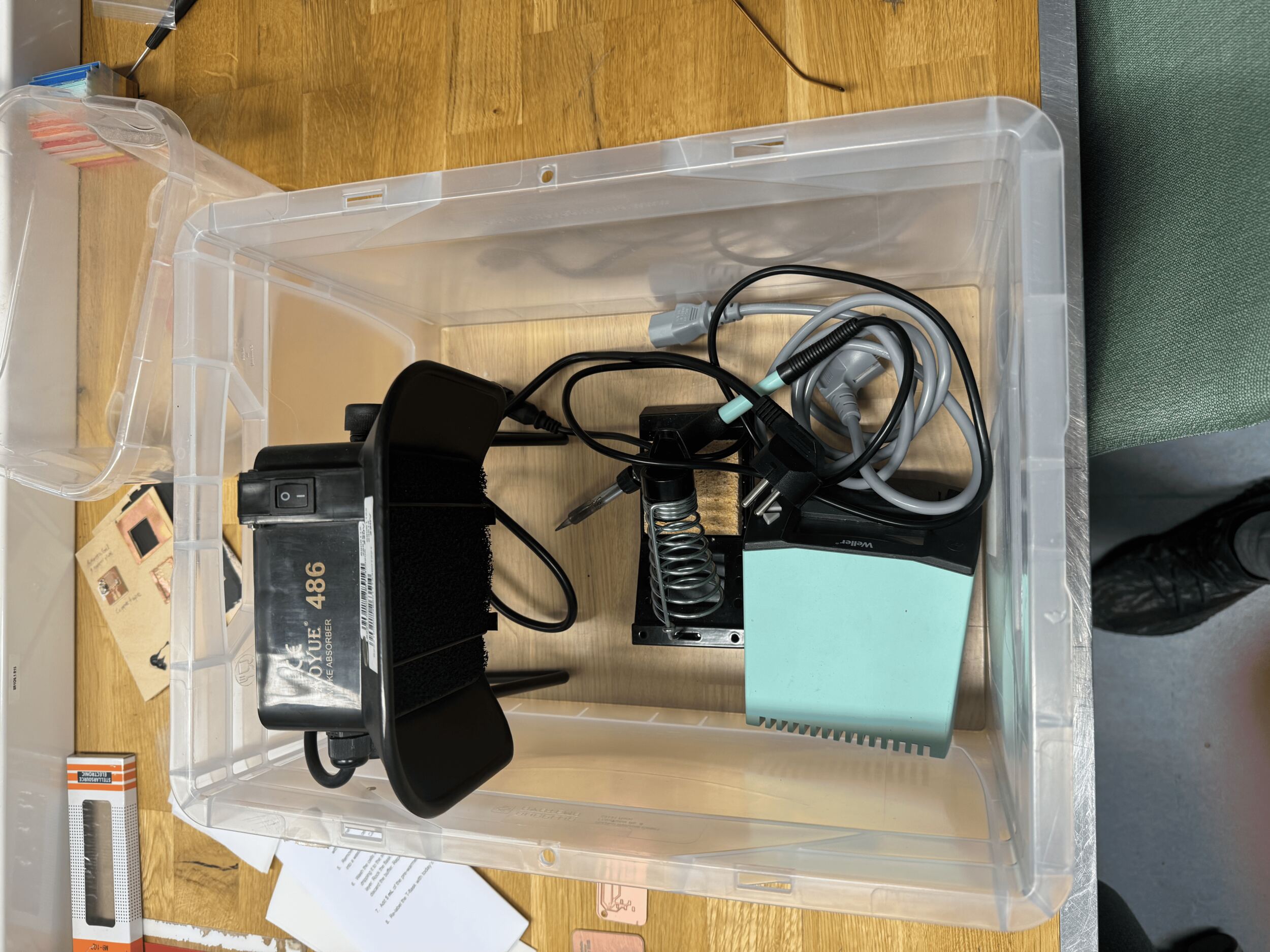
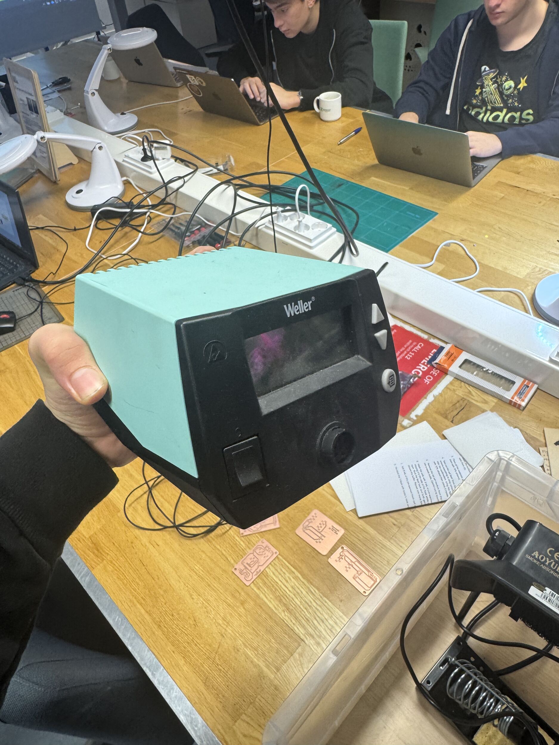
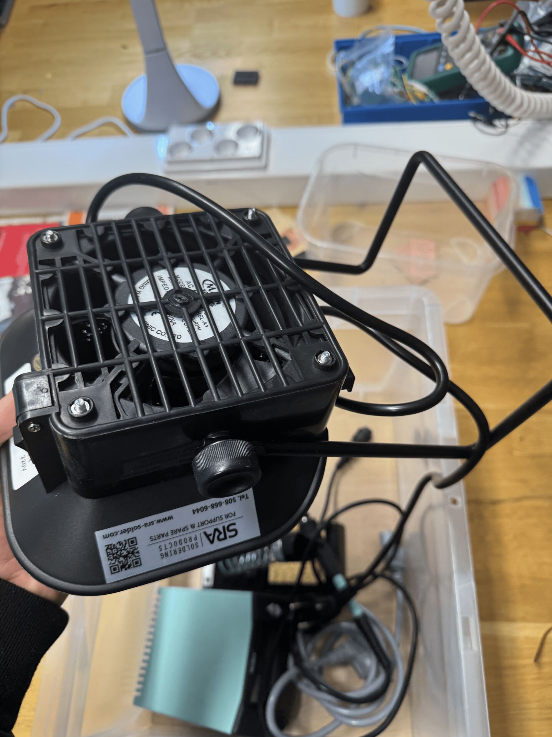
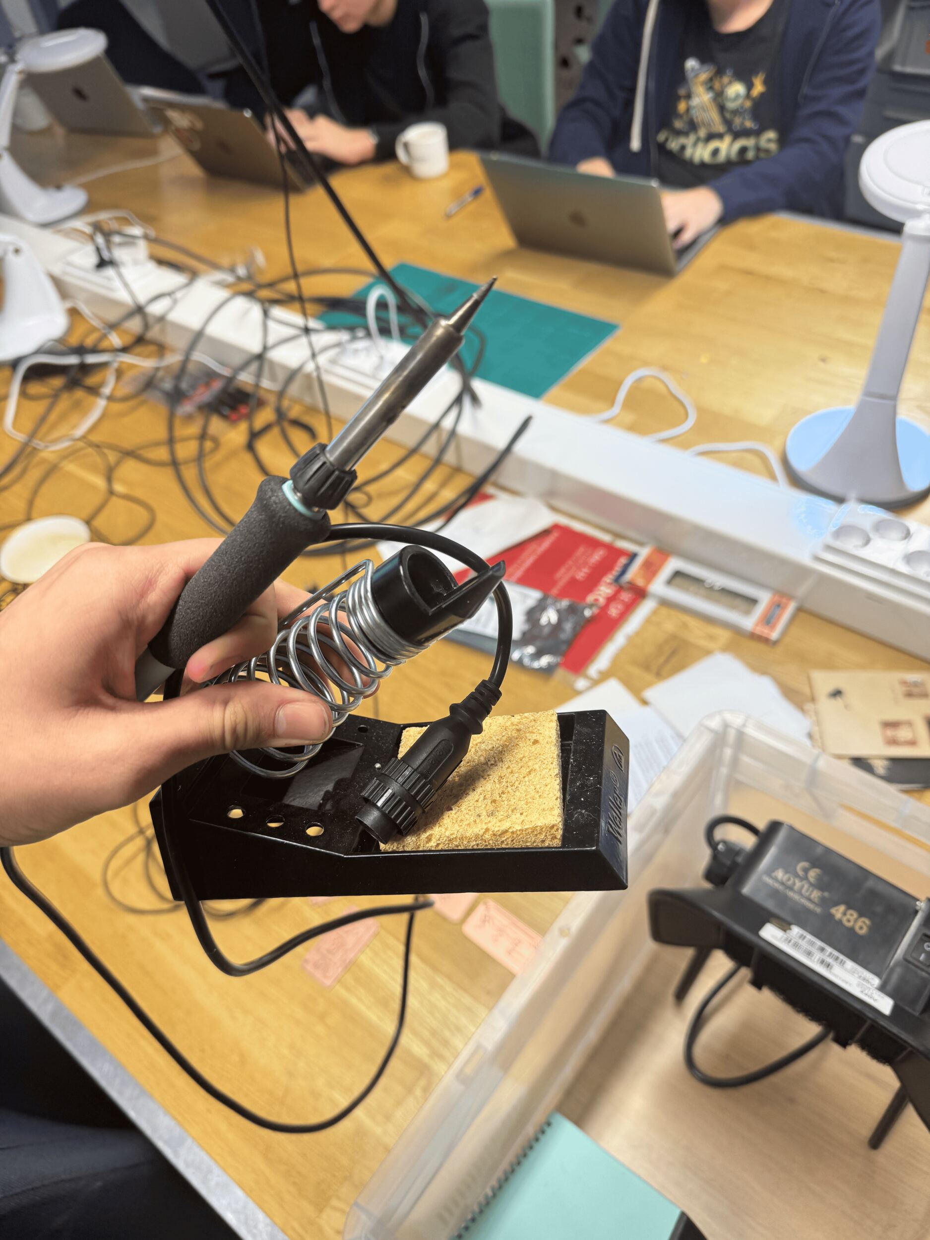
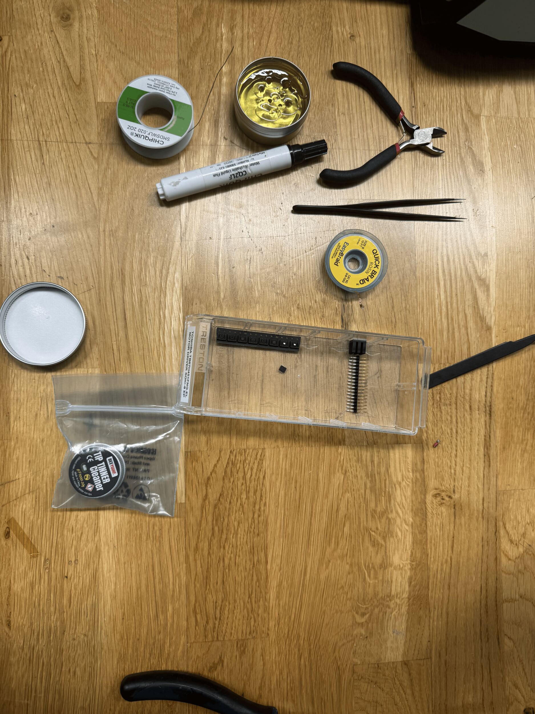
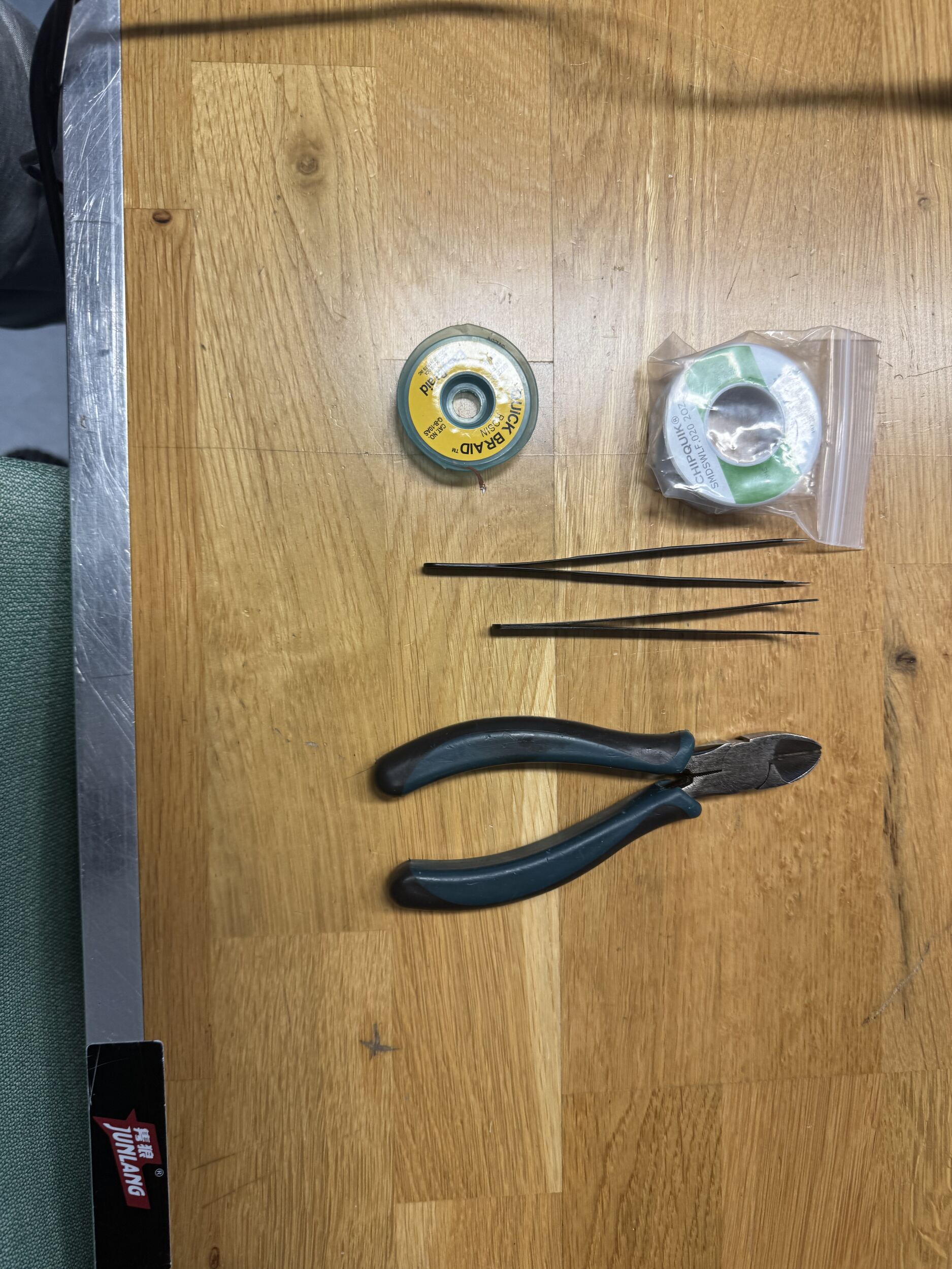
And I took a voice memo of Mr. Kris explaining the purposes of the items, and I listened to it to remember when doing soldering.
And I readied out a new board. Here are some photos and videos :
And this is my new board:
And i didnt like my old board because of that i did a new board with new settings:
And here are all the boards that I failed when I was trying to solder.
And after all of these boards and soldering problems, I changed my design and removed fillet corners and made the cabling better in the board. Here is the process:
And this is a trick about how to adjust the drill properly :
And this is my final board :
But I failed this board because I was a little bit harsh on the board, so I made another board and failed that afterward. In conclusion, I failed 8 boards because of soldering and adding too much power to the board, they all died because of me :((((.
But I didn’t give up and made a new one:
What i learned:
- I learned how to mill a PCB.
- I helped my friends and made them PCBs.
- I burned a seed and I got a new one and made it perfectly.
- Learned how to solder LEDs and Resistors
- Get a reflection from Mr. Kris and Mr. Sedat about my new PCB design (I think they loved it.)
- The last 2 boards took me an hour to make because I was learning how to use the machine
- I learned the hard way that I should be gentle with boards and pins.
- Learned new tactics in soldering.
- Gained experience in a few different ways (PCB soldering and milling).
This weeks group assignment: week-8-group-assignment