Week 06 - Electronics Design (KiCad)
KiCad Design
Schematic Design
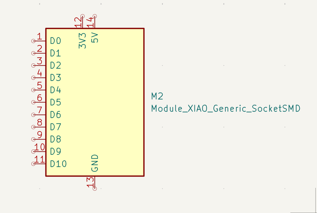
Firstly, I opened the “Schematic Editor” and “PCB Editor” to start creating a design for a system with a “Photo Sensor”. First, I added a “Module_XIAO_Generic_SocketSMD” to start.
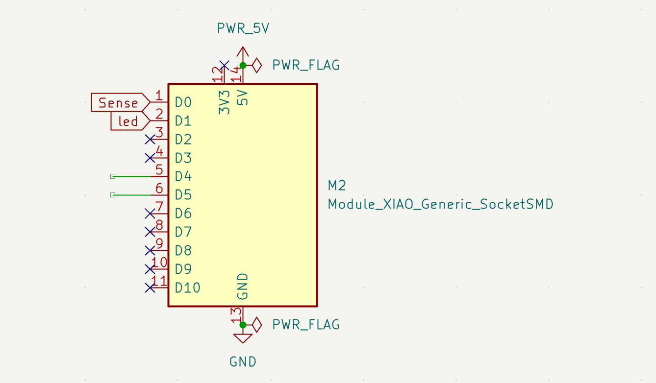
In the structure, I block the parts that are unnecessary. By pressing the key “Q” after touching the part, I don’t want to put an “X” on it, and “X” means no connection.
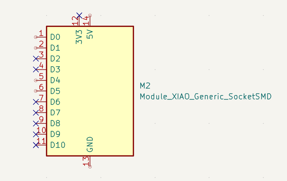
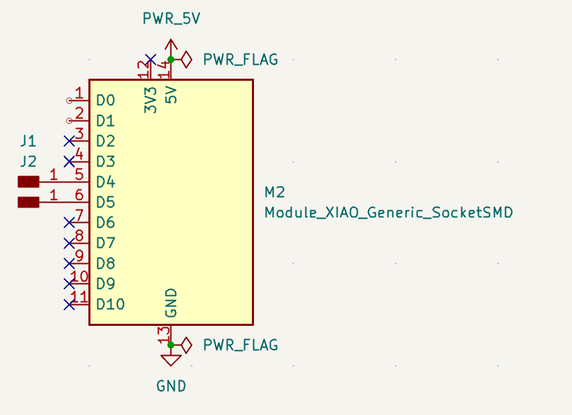
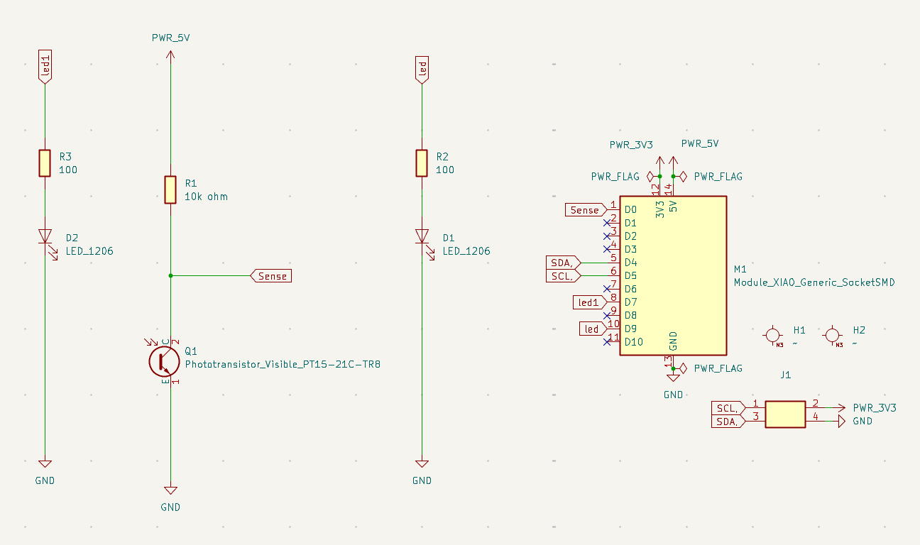
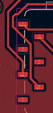
I left 1,2,5,6,13,14 open because I knew from the beginning that I was going to use them later on in the system. After that, I fill the 14th part with 5V and PWR_FLAG, and the 13th part with GND and PWR_FLAG. And the D4 and D5 with vertical headers.
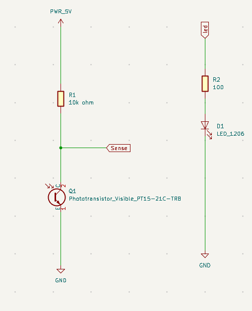
After all that, I realized that I didn’t do anything about the photo sensor that has the number “PT15-21C/TR8”.

I browsed this sensor and wrote KiCad after it to look at how to make a connection with it, and I saw this picture, and I know that I could use it.
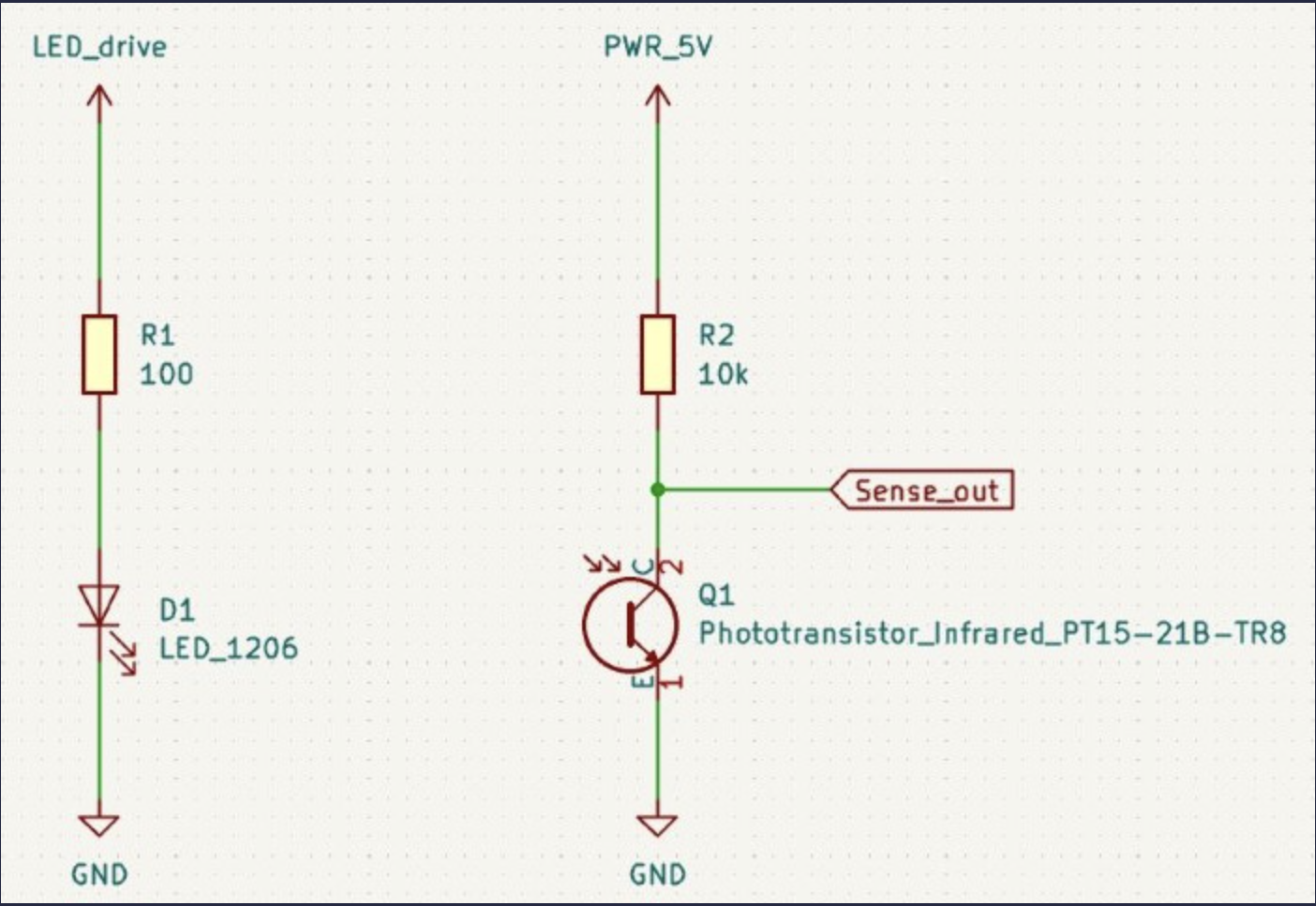
After I see this, I take this as an inspiration and start to do it.
As you can see in this, I changed the “LED_drive” with an LED flag because it would be easier for me to connect both with flags, and this is the flags combined part.
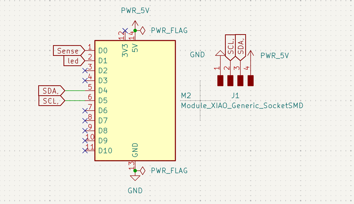
If you ask me why you make D4 and D5. I realized that I should make the connection vertical and with 4 headings, and I used 2 flags named “SDA,” and “SCL,” and used these flags at 4 vertical heading parts and empty D4 and D5 parts. And at the 4 vertical heading parts, I use a “GND” and “PWR_5V” to label the parts.
Additionally, when Mr. Kris had a quick look at this, he wanted me to change the “4 Horizontal Headers” with new vertical ones, and add 2 holes. This is how it turned out.
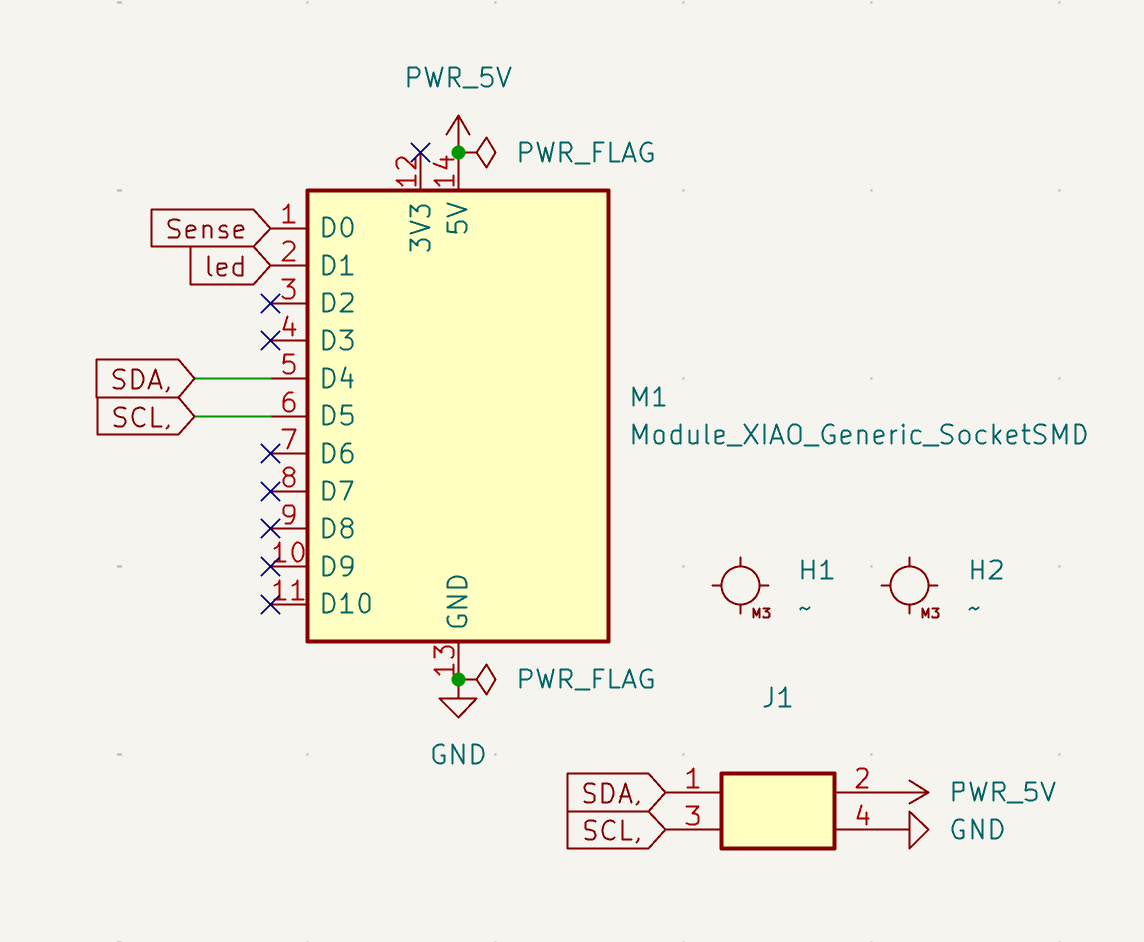

And I changed my schematic accordingly to this change once again. Here is my new schematic.
PCB Design
When I finished the “Schematic,” I directly started the “PCB” design. And because I didn’t want to do anything again, I pressed this button that converts “Schematic” to “PCB”.

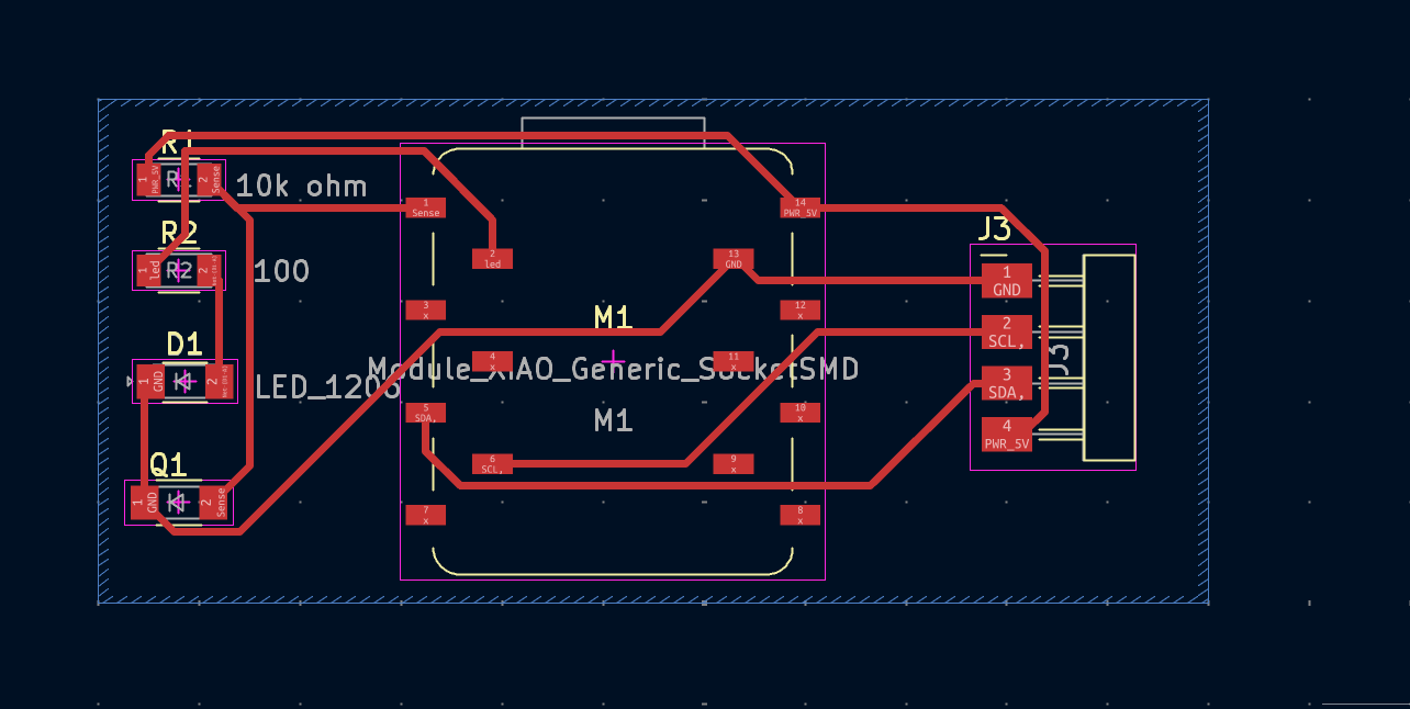
After all that, something like this came to my screen. (C and O are my initials)
This was the first model before making any changes at the “Schematic Design” and you can see that there are red parts and the outermost white part. I did the red part by clicking this button and then select “F.Cu” as the “layer” and “net” as “GND”.

The settings should look like this:
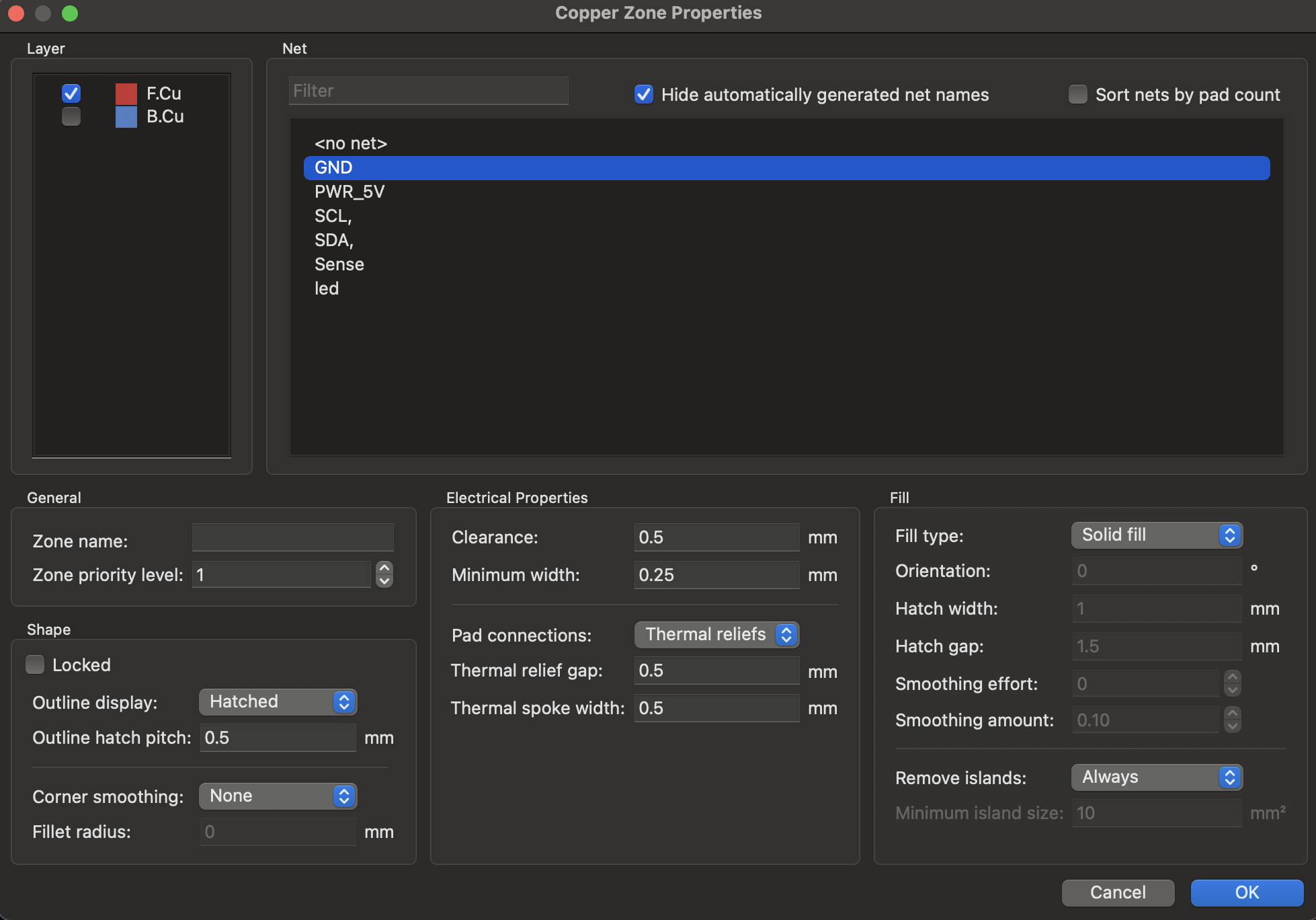
Lastly, do a right click at the red part and click on “Zone”, then “Fill the selected zone” And I did the white part by clicking this button and by selecting “Edge.Cuts” from the right side. But an obvious mistake that I made and didn’t realize was not connecting “GND” with the board, but with the cable.

Alongside this, when I do this my dear TA Omer told me that I should make the board bigger because that would make the soldering part easier, because it would give me more space to work on.
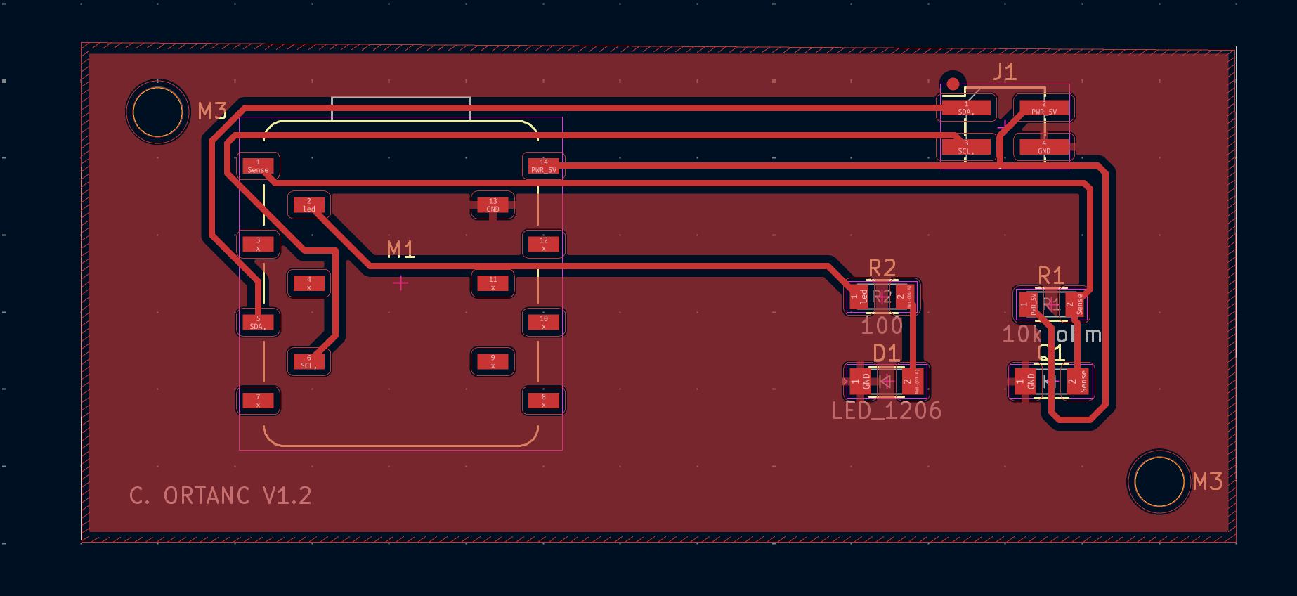
And I did the same steps in creating the red and white part, and this is how it changed.
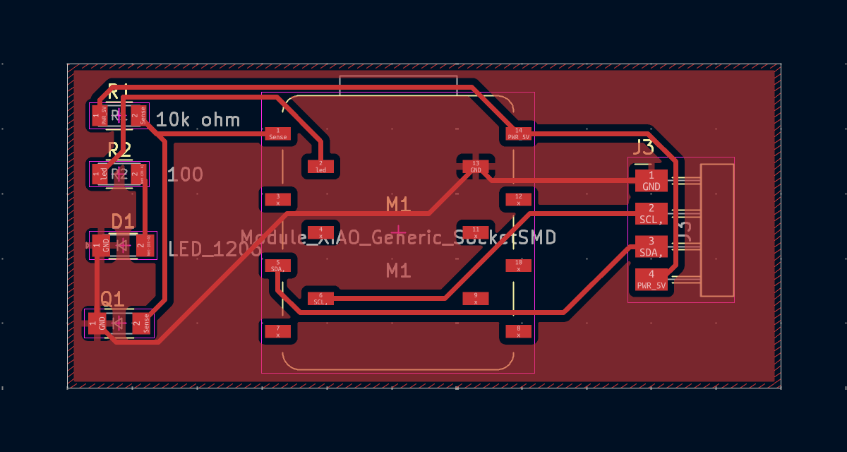
Finally, I changed the PCB design accordingly to “Schematic Design”, but I still had the same problem with the GND and the board. This is my first attempt to fix the problem, and the new board look in the PCB.
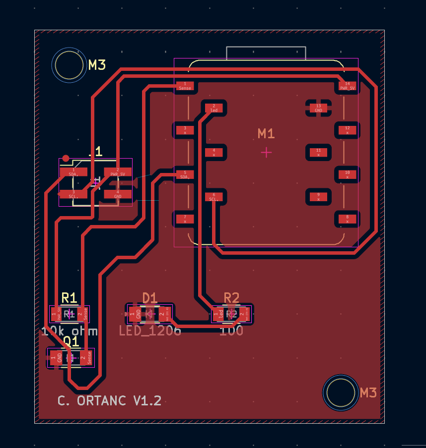
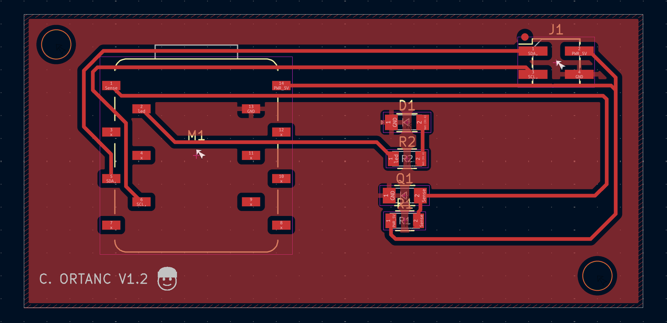
This is the second.
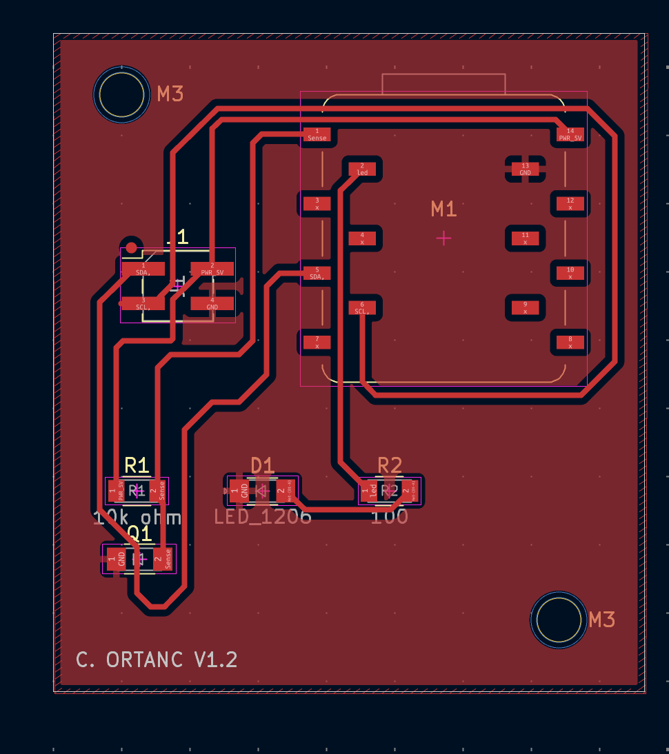
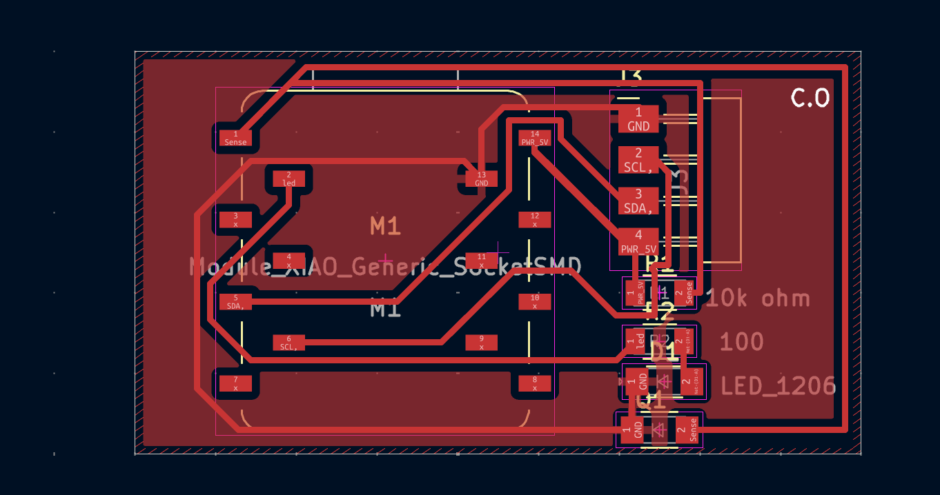
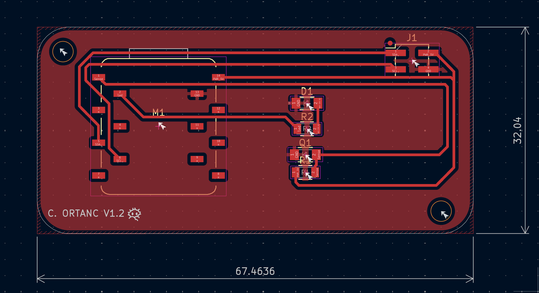
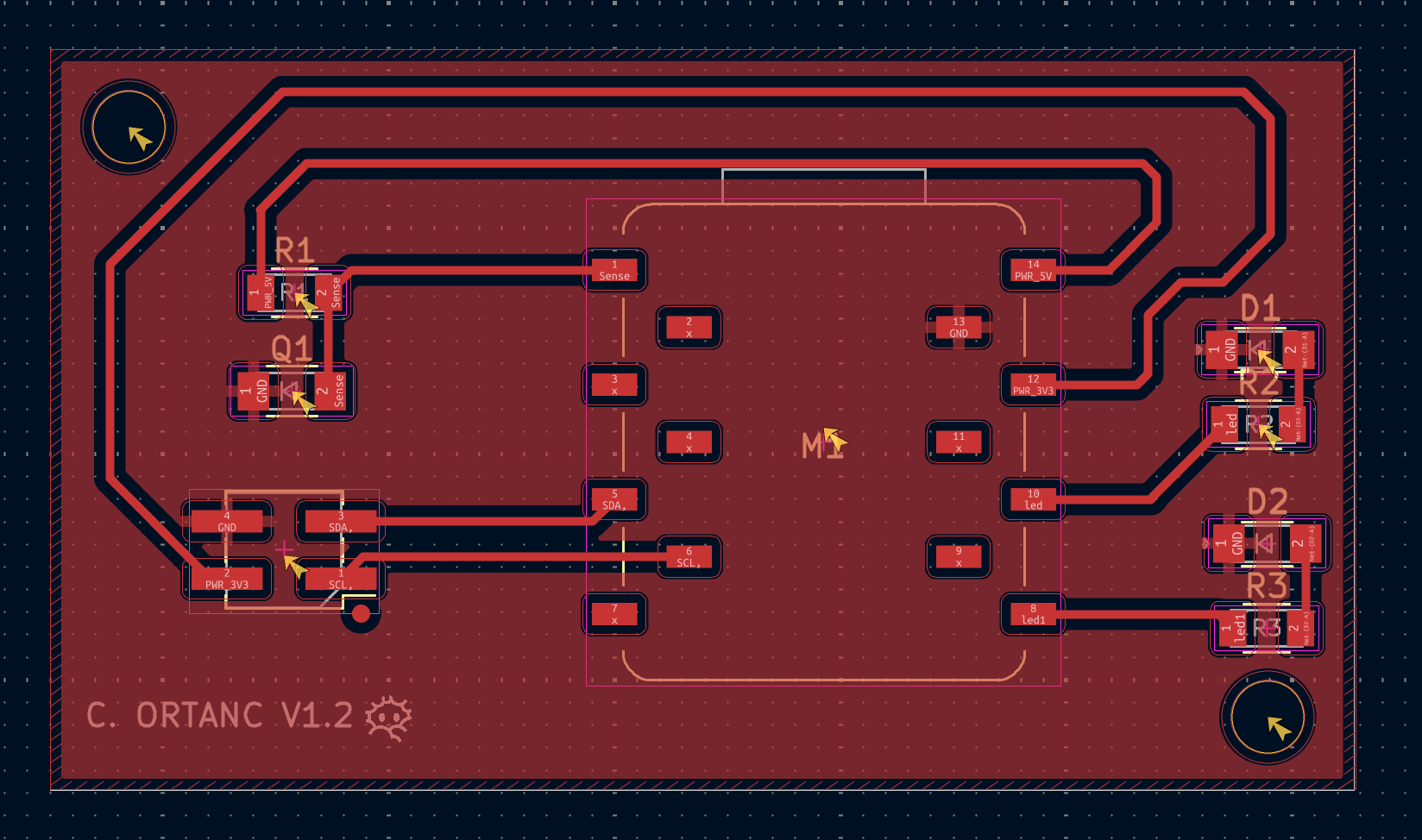
And this is the most successful and current one of the “PCB”.

And this was the final product of mine, “PCB”, with a small detail of my name on it!
PCB Design
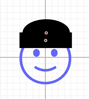
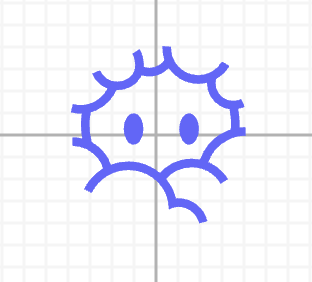
After I finished the fusion, I started to do a design for my PCB board and did a star at the middle of the board. But when I told our TA Omer my plan to draw a star, he rejected me and told me to do your design not with the lines in the PCB editor, but in Cuttle or some other design program. After my quick chat with Omer, I logged in to the cuttle and made a man smiling while wearing a beanie because Finland is cold :). And it looked like this.
But I had a little problem, I didn’t know how to add a Cuttle design into the PCB. Because of that, I get some help from Omer, and he told me that I should download my design as a .svg and then import it as a graph into PCB by clicking this at the same time.

When I clicked a menu, this popped up.
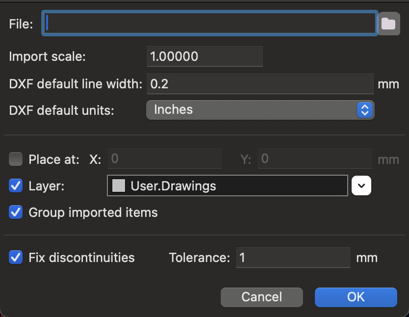
I put my file into the file section, and when I clicked OK, my design appeared on my screen like this.
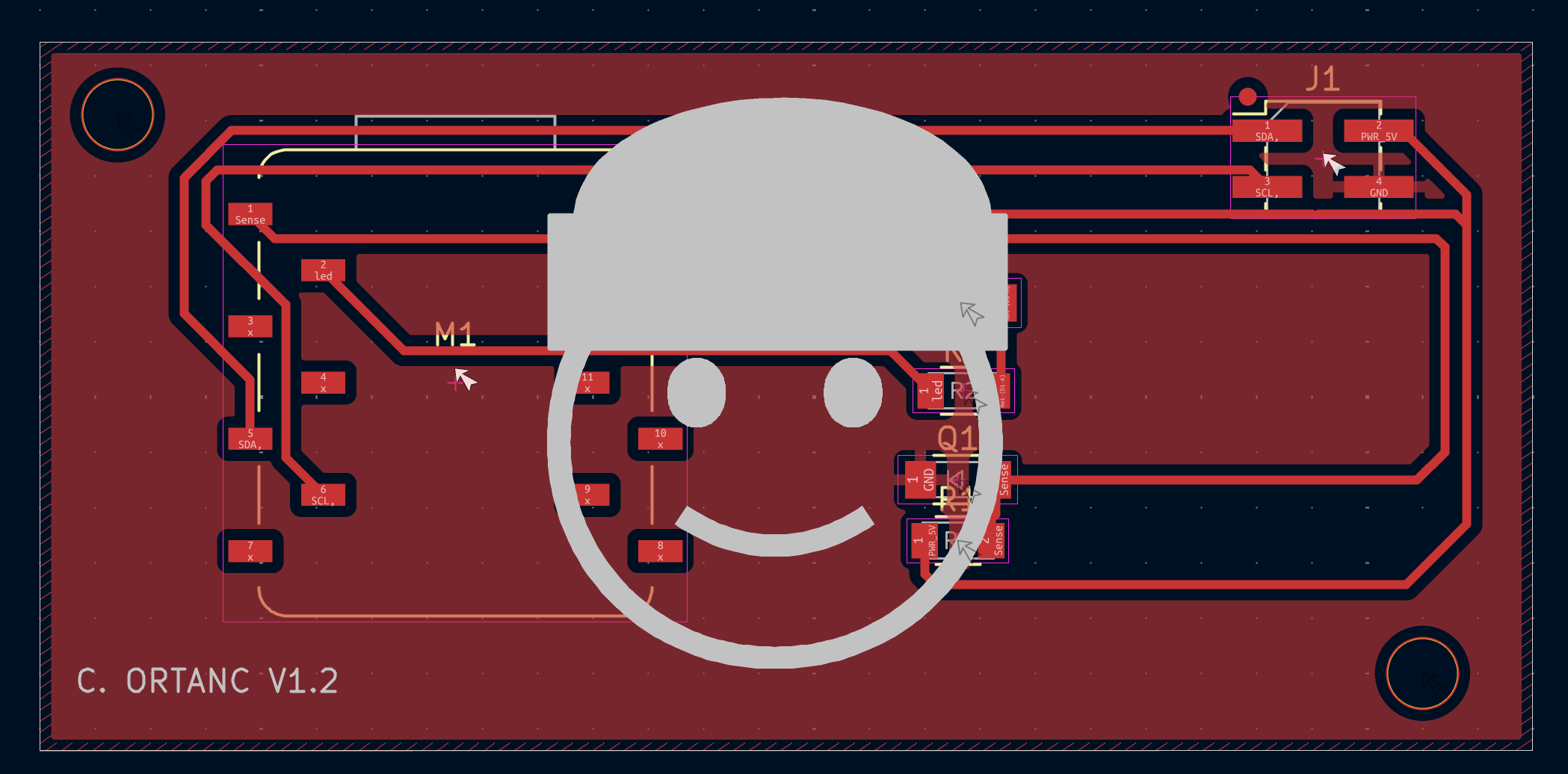
Yeah, it was massive, but I didn’t panic. I just changed the import scale from 1.00000 to 0.10000, and it turned out to be a great idea. This is how it looks after the scale change.
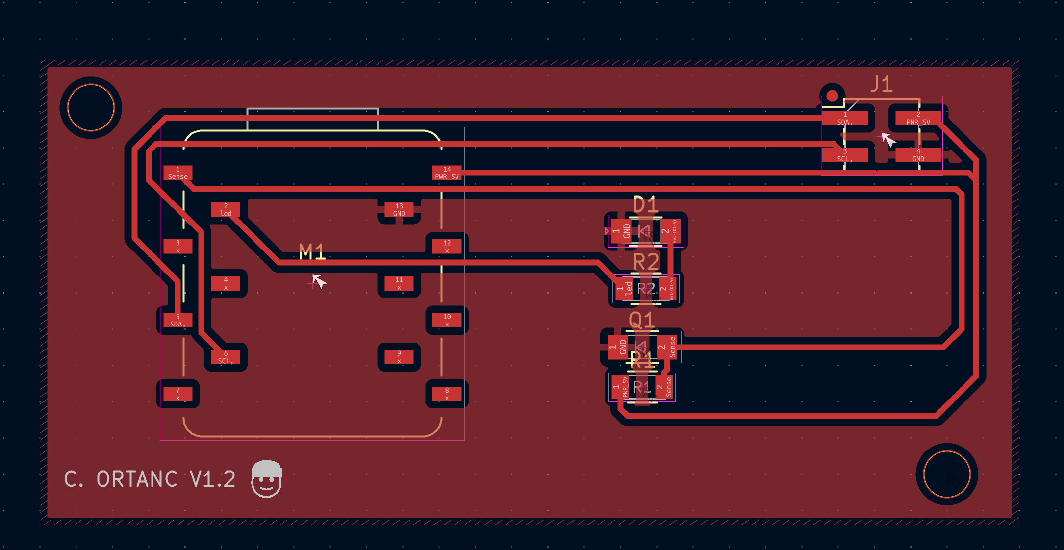
Yeah, you see the little guy at the bottom left, he is sweet, right? Besides the design, I changed the cable a little bit and put the sensors more in the middle of the platform, and I made the board smaller to not waste any copper board. This is before and after.
Before:
After:
And that’s all I did at the PCB part for now. Time 11.51 AM. When I started again, Mr. Kris told me that the guy with the beanie would be hard to put on because of that. I changed the guy in the beanie to the guy in the bush with the same things that I did when doing the guy in the beanie, and this is how it turned out.
New guy:
New guy in his new home!:
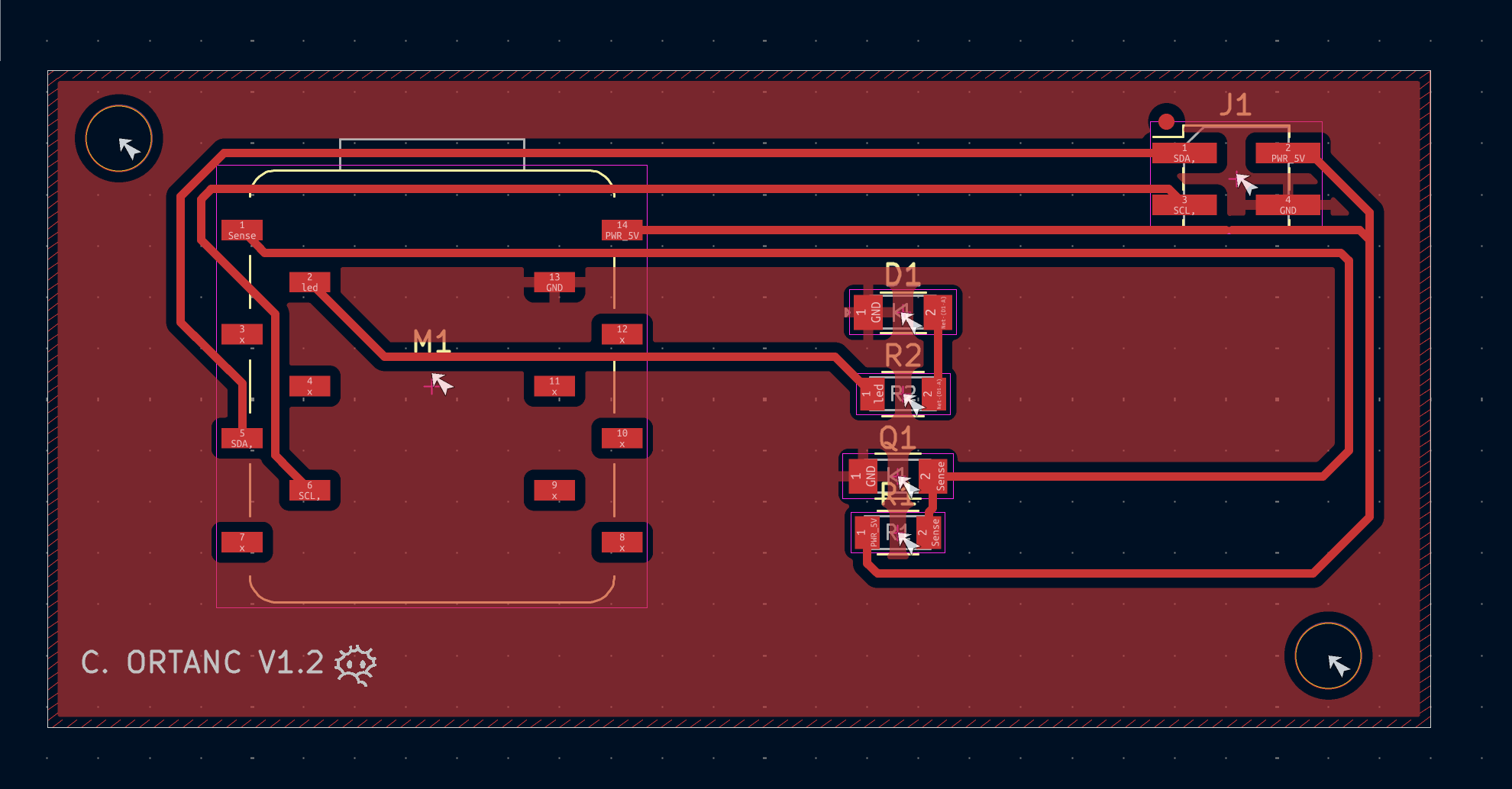
You see the guy at the bottom left? He is hiding in the copper on the PCB!
After this, I learned from Mr. Kris that actually, you can make the PCB’s corners curved, and you can see the measurements of the lines of the PCB, and I gave it a shot, and this is how it looked.
Now here is the how-to part. If you want to do the curved lines, you right-click at the white outer border and choose “Shape Modification” and then click “Fillet Lines…”. And if you want to see your measurements of your lines. Firstly, you should click this button and then click the top corner of the part you measure, and then the bottom corner, and click one more time anywhere you want to display the value.

After that, I made the area between cables bigger and with more area, and this is how it looks.
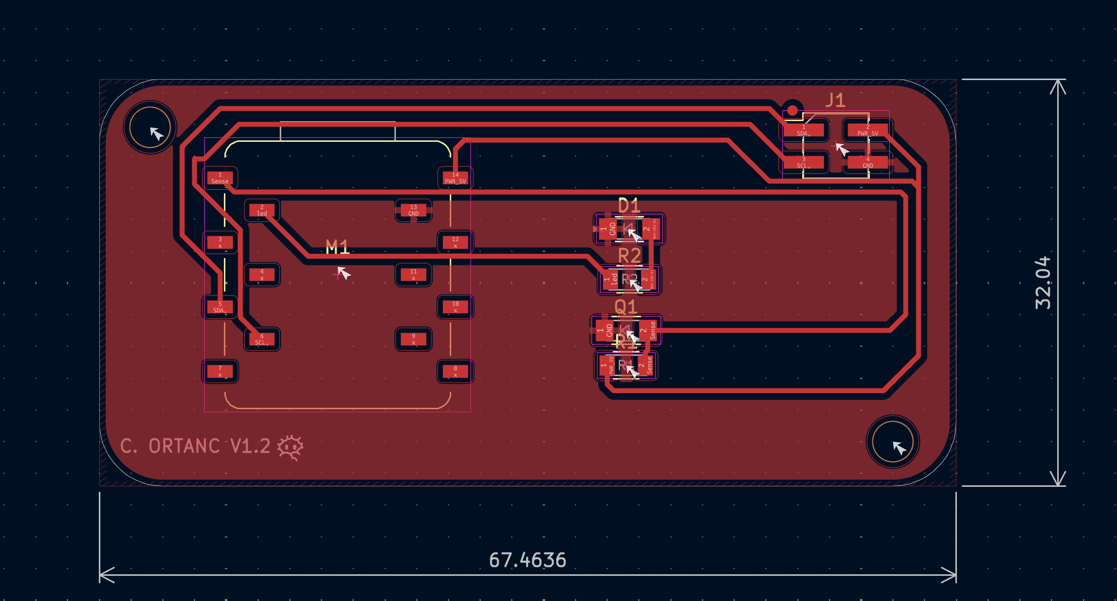
And I changed the design one more time because I predicted that it would be hard to solder it:
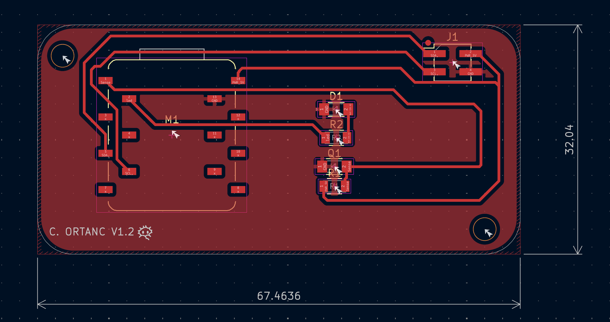
Firstly, the spacing was too small because the board size, and it was hard to do all of the panels of the board that got in the way of success. And there is the main part that creates the problem at the board, and here is how I fixed it.
I changed it once more because the line between 5, 4, 3, 2 creates most of the problem; it was creating a massive problem to be consistent with it. Because of this problem, it was obvious that I should change everything in the board, especially the milling part, and here is how I changed it:
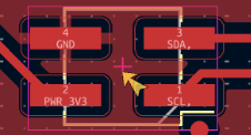
You see, I changed the structure of the board’s outer and inner layers, and I also changed the connection of the vertical header from 5V to 3V3 and moved the LED from 2 to 10. And didn’t use any cables between the 2 components because we don’t want to get new problems in the future when soldering parts (yellow arrows are there because I changed libraries mid-design).