Electronics Design
Group Assignment:
  • Use the test equipment in your lab to observe the operation
    of an embedded microcontroller
Individual Assignment:
• simulate a circuit
• use an EDA tool to design an embedded microcontroller system
  using parts from the inventory, and check its design rules for fabrication
• extra credit: try another design workflow
• extra credit: design a case
As usual, here is my schedule!

Group Assignment
Here is the link to Group Assignment : Link

Oscilloscope

An oscilloscope is a device used to visualize electrical signals as waveforms on a screen, showing how voltage changes over time. The X-axis represents time, while the Y-axis represents voltage. This makes it an essential tool for debugging electronics, checking sensor signals, and understanding signal behavior in real time.
The oscilloscope we used in our lab is the GDS-1202B by GW Instek — a digital storage oscilloscope, which means it can store and display waveforms for later analysis, not just live signals.
Key Controls:
- Power Button – Turns the oscilloscope on/off.
- Vertical Scale Knobs (Volt/Div) – Adjusts the vertical scale (volts per division) of the waveform.
- Horizontal Scale Knobs (Time/Div) – Adjusts the horizontal scale (time per division) of the waveform.
- Trigger Level Knob – Sets the trigger level for waveform synchronization.
- Trigger Source Button – Selects the input channel for triggering.
- Auto Setup Button – Automatically adjusts oscilloscope settings for optimal waveform display.
- Cursor Measurement Buttons – Enables measurement of parameters such as voltage, time, and frequency using on-screen cursors.
- CH1 / CH2 Buttons – Selects which input channel to display.
- Run / Stop Button – Starts or freezes the waveform display.
- Save/Recall Buttons – Allows saving and recalling of waveform settings and data.
- USB Port – Facilitates data transfer and storage via USB connection.
How We Used It:
To test the oscilloscope, we connected a sound sensor to a circuit and observed the resulting waveforms. We noticed the following patterns based on sound input:
- Louder sound → taller waves (higher amplitude)
- Softer sound → shorter waves (lower amplitude)
- High pitch → waves close together (higher frequency)
- Low pitch → waves farther apart (lower frequency)
- Different sounds → different wave shapes
We also observed both digital and analog signals to compare how they appear as waveforms on the oscilloscope screen.
Multimeter

A multimeter is a versatile measuring instrument that can measure multiple electrical properties — essentially a Swiss army knife for electronics. It can function as a voltmeter, ammeter, and ohmmeter all in one device.
What a Multimeter Can Measure:
- Voltage (V) – Measures electric pressure across a component or power source. (Red probe to +, black probe to –)
- Current (A) – Measures how much electricity is flowing through a circuit. (Connected in series — break the circuit and let current flow through the meter)
- Resistance (Ω) – Measures how much a component resists the flow of electricity. (Circuit must be turned OFF)
- Continuity – Checks if a wire or connection is complete. (Beeps if the path is good)
Some multimeters can also test diodes and measure capacitance.
Quick Reference for Use:
| Measurement | Connection Method | Circuit State |
|---|---|---|
| Voltage | Probes across component | ON |
| Current | Probes in series | ON |
| Resistance | Probes across component | OFF |
| Continuity | Probes across wire/connection | OFF |
Reflection
This week's group assignment was genuinely one of the most engaging sessions we've had so far. Having our local instructors, Dawa and Yangtshel, walk us through the oscilloscope and multimeter made a huge difference.
What stood out most to me was how the oscilloscope made electricity visible. Concepts like frequency, amplitude, and signal behavior that once felt abstract suddenly had a clear, physical representation on the screen.
Using the multimeter also reinforced how important it is to understand how you connect a measuring tool — the difference between measuring in series vs. parallel, or remembering to turn the circuit off before measuring resistance, are small details that matter a lot in practice.
Doing this group assignment with our classmates as well helped us work on collaboration and communication skills as we discussed why something was happening, shared insights, and worked together to come to an actual conclusion that made sense (to us).
Individual Assignment
Hero Shot

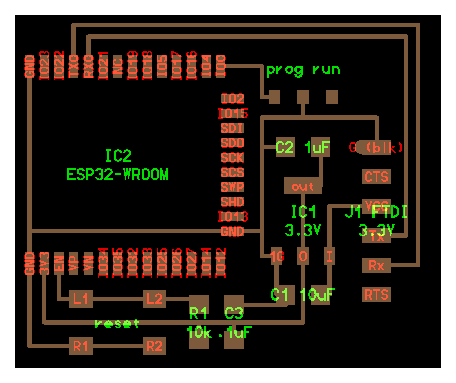
So for this week's assignment, I wanted to do something that I could actually use for my final project. I decided to make my final project board. I was planning to make it using the XIAO ESP32 S3, but unfortunately our lab doesn't have that right now, so I just went ahead with the ESP32 Wroom 32D board instead.
During our pre-fab time, we got introduced to the basics of KiCad. So I figured, why not keep going and learn more about it?
What is KiCad?
KiCad is a free, open-source tool that lets you design electronic circuits and Printed Circuit Boards (PCBs). Basically, it lets you draw out your electrical schematics and then smoothly move on to designing how the actual physical board is going to look — like where each component goes and how the traces are routed.
Before I Start — Libraries and Footprints
Before jumping into the design process, I think it's important to first understand what libraries and footprints are.
Libraries
In PCB designing, libraries are basically collections that store schematic symbols and footprints. They represent electrical components and how they physically sit on the board. The cool thing about libraries is that they keep everything consistent — so you don't accidentally pick the wrong component across different projects.
Footprints
Footprints represent the physical layout of an electronic component. They define the actual size, shape, and pad placement for soldering. Making sure your footprints match your schematic symbols is really important because it ensures that your electrical connections are correct and that your physical components actually fit and work during soldering.
Let's Start!
Before we start here are some Shortcut keys that I found Useful in Kicad.
KiCad Shortcuts
| Key | Action |
|---|---|
| A | Add component/footprint |
| M | Move item |
| R | Rotate component |
| W | Wire (Schematic) / Route Track (PCB) |
| V | Add via (PCB) / Edit Value (Schematic) |
| E | Edit component properties |
| C | Copy component |
| Del | Delete item |
| Esc | Clear selection/cancel |
| Spacebar | Set relative coordinate origin |
| Ctrl+S | Save project |
I reinstalled KiCad and here's how I did it.

First, go to the KiCad Download Page and download the latest version.

After that, just follow the instructions on the screen and install it on your computer.

After that, I downloaded the fab libraries from this link.

To import them, I opened KiCad and clicked Preference > Manage Fab Libraries. Then I selected the fab libraries and imported them.


Components
| No. | Component | Qty |
|---|---|---|
| 1 | 0Ω | 9 |
| 2 | 100nF | 5 |
| 3 | 10kΩ | 8 |
| 4 | 10µF | 1 |
| 5 | 1µF | 2 |
| 6 | 330Ω | 1 |
| 7 | 4.7kΩ | 2 |
| 8 | 499Ω | 2 |
| 9 | AMS1117-3.3 | 1 |
| 10 | Conn_PinHeader_FTDI_1x06_P2.54mm_Horizontal_SMD | 1 |
| 11 | Conn_PinHeader_UPDI_1x02 | 2 |
| 12 | Conn_PinHeader_UPDI_1x02_P2.54mm_Horizontal_SMD | 5 |
| 13 | ESP32-WROOM-32 | 1 |
| 14 | LED_1206 | 1 |
| 15 | PinHeader_01x04 | 3 |
| 16 | Switch_Slide_RightAngle_CnK | 1 |
| 17 | Switch_Tactile_Omron | 1 |
Schematic Design
Once everything was set up, I started my design process. I created a new project and opened the schematic editor.


This is the KiCad Schematics Interface.

Using the Place Symbol (A) tool, I placed all my components on the schematic.

I started off by making the basic ESP32 Wroom circuit, but then I realized I also needed to add pins for my other components.

After that, I reconnected all the components and the schematic ended up looking like this.

Now that everything was connected, I ran the Electrical Rule Checker to check for any issues with my circuit. I got 1 error and had to do some fixes. (I removed the PWR_FLAG symbol ^-^)


I ran the test again and got no errors. Yay!! Though I did get a bunch of warnings telling me to add footprints for the components.
I used the Assign Footprint tool to add the footprints as shown below.


Yay!! Only 6 warnings left, which are fine to ignore.

This is the final Schematic Design.
PCB Routing
After finishing the schematics, I moved on to PCB routing.


In the PCB editor, I first set the Trace Width:
- 0.4 mm = For Signal Traces
- 0.6 mm = For edge cutting traces and Signal Traces
- 0.8 mm = For Power Traces


After that, I started routing the traces. Honestly, this was the hardest part of all my previous assignments because I had so many components to route. (It took me 10 hours to route everything using nine 0Ω resistors ^...^)


After 10 long hours, I finally finished it. Yay!! 🎉
Mods CE
After that I exported my PCB as a SVG file.

Then I imported the image into Inkscape and made the EDGE and the Interior files. This is how I did it:


I went to the document properties and clicked fit to design.

After that, I ungrouped the shapes and expoerted the different files in SVG format.


I then imported the files into Mods CE
In my lab We have the Roland SRM 20 milling machine and I chose the following settings.
Programs -> mill 2D PCB


This is the interface you should get to start making the RML file for the PCB.

First I imported the SVG file and Click Invert

Then I chose the 1/64 for the mill bit size

After that select the 2 programs and click the delete button.

I then created a new module( save ) Modules -> Save

Then Join the modules together like shown above.

After that Click CALCULATE!!

After calulating your file will be automatically be downloaded to your computer and you can view the tool path by clicking the VIEW button like shown above.

Yayyy this is my toolpath for the PCB!

After that we have to do the same process for the EDGE cut but the only difference is that in the mill bit size its 1/32 instead of 1/64.


After clicking the calulate button you will get the toolpath and the RML file for the EDGE cut.

Yayyy this is my toolpath for the EDGE cut!
This is how my PCB will look like after millling. Not Gonna Lie it looks pretty good.

Reflection
This week has honestly been the most time consuming and frustrating week so far, but it also came with a ton of new knowledge, experience, and a good lesson in resilience. Especially during the PCB routing, that part was a complete nightmare. It literally took me 10 hours to finish. My initial goal was to route the entire circuit without using any 0Ω resistors, but I ended up using 9 of them. Oh well.
On the bright side, I'm really happy that I got to learn a lot about circuits and even some physics behind resistors, capacitors, and the components themselves. On top of that, I got to design my very first board for my Final Project, which honestly feels like a huge achievement for me.
From here on, I plan to keep going with the same energy and dedication — and honestly, I'm lowkey looking forward to the next nightmare. ^0^!!
Files
References
Hello.ESP32 Wroom 32 Schematics
That's it for this week. See you next week!