Week 08: Electronics Production
Group Assignment
- Characterize the design rules for your in-house PCB production process: document the settings for your machine.
- Document the workflow for sending a PCB to a boardhouse
- Document your work to the group work page and reflect on your individual page what you learned
Click here to see our group page.
In class we followed this MakerCAM Workflow to create the toolpaths for making a PCB on the Carvera. We did not drill any through hole connections. Mr. Dubick would like us to use surface mounted soldering.
We were given an edge cut and F_Cu .gbr file. Even compressed, together they are 8KB, so I will not attach them here.
Key notes:
- .8mm Corn flat-end bit is used to remove the bulk of the material
- The .2mm*30ºEngraving(Metal) engraving bit will be used to cut out the copper traces
- The Makera Milling machine affixes the FR4 using clamps, rather than adhesive, so tabs are necessary to keep the PCB in place.
- 2D contour is used for edge cuts
- 2D pocket is used for copper traces
- 2D drilling is used for drill holes
PCB Toolpath Workflow on MakeraCAM
-
Open Makera CAM and select New Project
- choose 3 AXIS project on the welcome screen, since we are not rotating
-
Set the stock in the "Stock Setup" panel on the left
- click "Edit"
- enter dimensions of your PCB stock:
we used this standard size of FR4 boards available in our lab. Should I use a different board, I would need to measure the dimensions.
- Material: PCB
- Length (X): 127 mm
- Width (Y): 101 mm
- Height (Z): 1.7 mm

- click OK to save
- In the top toolbar, click the icon titled “import PCB” and individually insert all Gerber files into the workspace.
- The imported gerbers will likely populate outside of the workspace, so select all 2D layers, hover over the “Adjust object” and “Transform” drop-down menu and select the “Move” tool

 When layers are dotted, that indicates that they are selected; when layers are solid, that indicates that they are unselected
 - Select the bottom left corner as the anchor point
- Set both the X and Y location values to 6 mm, which positions the file in the bottom right corner of the workspace

This image shows that my pcb is way too big. I stopped, and spent the rest of the night working to resize my pcb. I hoped that Claude would be able to help, but as I feared, after may hours, I had to do remake on KiCad from the schematic.
I worked in Claude.ai to detail the attempt to fix the problem, and create a markdown document with screenshots referenced, and saved in a separate folder. Click here see that document.. The document ends when I realized Claude could not fix this, and I restarted from KiCad. Click here for the chat transcrip and screenshots
continuing on with my smaller pcb design: I made sure to take many screenshots, but I can't find them!
- Keeping all layers selected, hold the shift key and deselect the outer edge of the Edge_cuts
- Toggle the visibility such that only the “F_Cu” and the “Edge_cuts” layer are visible
- In the top toolbar, hover over the “2D Path” drop-down menu and select the “2D Pocket” option
- In the dialogue box, adjust the “End Depth” value to .05mm
- Under “Tools,” click the “Add Tool” button, select “.8mm Corn tool” and click “Choose”
- Click “Add Tool” again, select the “.2mm*30ºEngraving(Metal),“ and click “Choose”
- Ensure that the material selected is “PCB”
- Click “Calculate”; you should see a “2D Pocket” toolpath fall under the Path dropdown in the hierarchy
- If you have drill files, untoggle the visibility for all “F_Cu” and “Edge_cuts” layers and toggle visibility for all drill files
- In the top toolbar, hover over the “2D Path” drop-down menu and select the “2D Drilling” option
- In the dialogue box, adjust the “Drill Tip End Depth” value to 1.7mm
- Under “Tools,” click the “Add Tool” button, select “.8mm Corn tool” and click “Choose”
- Click “Calculate”; you should see a “2D Drilling” toolpath fall under the Path dropdown in the hierarchy
- To design a toolpath for the edge cuts, untoggle the visibility for all drill files and toggle visibility for solely the “Edge_cuts” layer
- Select the inner outline of the “Edge_cuts” layer
- In the top toolbar, hover over the “2D Path” drop-down menu and select the “2D Contour” option (synonymous with a “Pocket” cut)
- In the dialogue box, adjust the “End Depth” value to 1.7mm
- Under “Tools,” click the “Add Tool” button, select “.8mm Corn tool” and click “Choose”
- Under “Strategy,” select “Outside”
- Under “Tabs,” select “Custom,” and click “Add”
- Add appropriate tabs around the selected “Edge_cuts” layer (typically, 3 will be sufficient)
Tip: Ensure that these tabs are staggered and not directly across from one another
- Click “Calculate”; you should see a “2D Contour” toolpath fall under the Path dropdown in the hierarchy
- In the top toolbar, click the icon “Preview Toolpaths,” and select all toolpaths in the pop-up dialogue box
- Click “Preview” and press the play button to view a simulation of the toolpaths
- In the top toolbar, click the “Export” button, ensure all toolpaths are selected, and click “Export”
- Rename the .nc file to your last name, your first initial, and your project name, followed by “gcode”. This helps when pulling up your specific file on the FabLab's computer.
PCB Milling workflow using Carvera Controller
- Connect to carvera
- Once the toolpath .gbr files are downloaded onto the computer connected to the carvera, open the carvera program, and connect it to the computer by unlocking it from the top toolbar by clicking on the button with the status "N/A disconnected."

- Choose unlock.
 It will then be connected through COM3.
If this doesn't work you may need to restart the machine, the emergency stop may have been pressed.
-
In the menu in the top right corner, click “Switch to display manual control interface” followed by the “Home” button.
-
Check that the probe battery has enough power. The number marked in red needs to be greater than 3.6V. This is so that the machine operates properly in the z-axis.

-
Secure your material with the double sided tape in the center, and the clamps on the sides.

-
Check the vacuum to see if there is a clog and if the bin is full. I had a clog in my vacuum tube, but couldn't reach it to unclog it. I eventually got it by putting the vacuum directly to the vacuum nozzle of the machine. It sucked it back out!
This is me securing my material.

We are using FR1 board material because they are made with phenolic paper unlike FR4 that use fiberglass. It doesn't conduct heat like the FR4 boards so you must use heat from above to do surface mounting.
-
In the bottom left corner, open the G-code from your files.
-
Before starting the mill, open the menu in the top right corner and click the “Switch to display file preview interface” to preview the toolpaths.
-
Click the gear icon on the bottom left, “Config and run,” the auto vacuum should be on, set work origin to match your material placement, and make sure auto leveling is on.

-
Double check your settings, and click "Run"
-
The machine first runs a laser over the edgecut to check placement. Make sure the laser does not go off the board.
Cutting the pcb:
After the pcb was cut I had to cut the tabs that we set to hold it in place as it was cut.


This week we were only able to use the CLS Fab Lab 1 day. We were planning on 2 days because the school is closed for spring break, which was bad enough. However, there was a big storm that dropped a tree on the powerlines, canceling our 2nd day. The lab will not be open until next Monday the 23rd. I tried to have some components sent home with my son so I could solder the components on at home, but they didn't make it. When I found out they hadn't made it home, I ordered some parts on Amazon to be delivered ASAP. They didn't make it before we left for our family trip.
I attempted to use the surface mounted soldering resistors and LED, but they were too tiny.

During the Global lecture I took this screenshot of that shows solders using different techniques. In conclusion, there are many ways to solder. It is personal preference as to which method you choose. A good solder joint is smooth and shiny.

Once I arrived home from vacation, I used the female headers I had shipped to attach the esp32-c6 microcontroller to the board we made in class. Mr. Dubick had said this was a blinking board, which would mean there must be a resistor and an led. I remember seeing a schematic that showed the circuit connecting to the 5v pin and p17. I used a resistor that measured 465 Ohms, and a red led.
I used my soldering iron and solder wire to attach the female headers. They did not look pretty.

I used soldering paste, and my embossing heat gun to connect the resistor.

I used soldering paste and the soldering iron for the led, and it did not work as nicely as the heat gun. The led kept falling over as I was not steady enough to hold it still, and the paste couldn't hold it like it did for the resistor. The soldering iron burnt the board a bit. I also couldn't make the solders nicer, because when I tried, the led would fall over.

I set up this code in Arduino IDE by starting a new sketch, choosing my board and location (esp32-c6, usb port), declaring my integers in, setting up my pin output through pinMode, and creating a digitalWrite and delay blinking light code. I just wanted to make sure it worked.
const int led = 17; const int quick = 500; const int slow = 1000;
void setup() { // put your setup code here, to run once: pinMode(led, OUTPUT); }
void loop() { // put your main code here, to run repeatedly: digitalWrite(led,HIGH); delay(slow); digitalWrite(led,LOW); delay(slow); digitalWrite(led,HIGH); delay(quick); digitalWrite(led,LOW); delay(quick); }
Since, I had not yet made a circuit like this one running from the 5v to an output/ input pin, I wanted to check to see if my hypothesis was correct. I think that connecting in this way will always have current running through the circuit so the led will dim, but not go off. For current to flow there must be a voltage difference, like water flowing downhill. This would mean that if pin 17 is set to HIGH 3.3v will be coming from that pin, and 5v would be on the other side of the circut. This has a voltage drop of 1.7v over the circuit, where as if pin 17 is set to LOW the voltage drop would be 5v. Therefore the led should be bright when pin 17 is set to LOW. I tested this with the following code that had the delay set to a much longer time for one digitalWrite(led,HIGH). The other delays were set to quick. This allowed me to see the pattern, and specifically when the pin was set to HIGH.
const int led = 17; const int quick = 500; const int slow = 3000;
void setup() { // put your setup code here, to run once: pinMode(led, OUTPUT); }
void loop() { // put your main code here, to run repeatedly: digitalWrite(led,HIGH); delay(slow); digitalWrite(led,LOW); delay(quick); digitalWrite(led,HIGH); delay(quick); digitalWrite(led,LOW); delay(quick); }
As expected the led was dim when the pin was set to HIGH.
Individual Assignment
Make and test a microcontroller development board that you designed
Since I only had 1 day in the lab this week I got creative in designing, and making my own pcb boards at home. I was able to build and test a 3d printed board coated in copper tape, and a sewn board that used lilypad components. I used my idea-pcb layout from week 6 in hopes that I will be able to mill the same board once I get into the lab.
The rest of the week I spent my time this week fixing up my documentation, as my global evaluation has brought it to my attention that files are missing in my early weeks from when I had so many GitLab issues.
Although it is frustrating that I couldn't get my board printed, and tested this week, I see the silver lining of being given the opportunity to look into different PCB board production techniques. This is what I find the most fascinating. I love learning the properties of materials, the chemical equations and reactions, and how we can use everyday items to make magic happen. For years I have been dreaming, sometimes literally, of different methods to make circuits.
I usually only allow myself to dive into a new scientific curiosity if I can relate it to my real work, my kids. Then I go deep! Last year I was inspired by rocks, and created the programming for "camp rocks" Girl Scout encampment that had over 200 scouts attend. I was able to show the scouts how piezo electric crystals are used to make fire by rewiring a lighter to a LED, so that when they clicked it the red light flashed. And they are used in some native american cultural traditions as they create cold fire when banged or rubbed together. As there was a high risk for wild fires during encampment, the scouts found much joy in seeing these sparks without having an actual fire.
Two years ago Mr. Dubick showed me how to wood turn pens. This led me to learn all about wood, carving, harvesting, treating, turning. I thought it would be fun to create magic wands with wood turned handles that the kids could fill with their choice of core material, and hid a small magnet in the tip. I also created small toys with magnets inside that were just the right weight and shape to move around without being obviously magnetic. The kids used their wands to practice kinetic spells with the toys. I called it rare earth magic as they used rare earth magnets. I also created an electromagnet with a coil of copper that completed a circuit when balanced upright. The kids used their wands to spin the coil. I hope to use my wands in my final project to control some circuits.
I want my magic table to use unusual ways of connecting simple circuits. I like the kids, and adults, to ask why and how the "magic" happens, and see the true wonder of science.
Soldering practice
In prefab Mr. Dubick went over soldering with us, and gave us practice boards to use. Here is my documentation on that practice, which I did at night while helping my mother after her surgery this fall. I traveled with my soldering kit in my suitcase, and was very worried I would get questioned by airport security because of it. Luckily, I had no troubles with security. I had created my documentation in a Pages document, which I copied into a .md file. I pulled each image and video from the document, then edited, and saved them in a folder. I had Claude.ai add them into my .md file after each image was referenced. I also learned how to edit my videos to be 4x speed, which I added to the end of my week02 video-compression.md.
Different PCB board production techniques I am curious about:
Copper taped 3D printed PCB boards
I found this tutorial on 3D printing a PCB board. 3D Print Your Own PCB by QZW Labs. The process is:
1. Open project in KiCad pcb editor.
- 2mm minimum trace width.
- route traces on the back copper layer. He does this to use through hole components, which make his board look very clean at the end.
- Through hole pad diameter at least 1mm
> I set these rules in the Board Setup so that I could see with the rule checker if my board met the criteria

    2. File -> Export -> STEP
        - check Export board body only under board options
        - Under conductor Options check only Export tracks and vias
        - Under Coordinates, choose Drill/ place file origin
        - Under other Options, check substitute similarly named files, Overwrite old file, Don't write P-curve to STEP file

    3. Open STEP file in Fusion
        - extrude traces 0.6mm

- also make them wider

Some of my traces did would not extrude. I used the push function to make them wider. If you don't do this, thin traces won't print.

 (or the traces can be indented)
    4.  Combine the layers of your pcb using the combine tool.

    5.  Save 3mf file, and open in Bambu 3D printer.  Follow these steps to get a better quality print.
        - in preview under Quality set "Wall Generator" to Arachne
        - in preview under Strength set "Top surface pattern" to Rectilinear

I used copper tape to cover the extruded traces.

Almost all the copper tape is trimmed off, but I needed to go to bed.

I soldered the led to the copper tape, and left the legs. I was then able to spread the solder out a bit along the leg to attach to the copper without melting the pcb.

I had troubles with the soldering, because the traces were so close, the tape thin, and the pla being easily melted. Fortunately also because the pla was easily melted, I was able to disconnect the shorted joints with repeated sweeps of my soldering iron.

In some cases it would melt the pla a bit, and create a channel through the solder. I was also able to melt the pla to hold some components more securely as I soldered, like the resistor.

Testing the circuit:
The button doesn't work, but the light is on!
the button doesn't work because I haven't added the resistor or programed it to do anything! I forgot that the switch was not inline with the light. It is an input device.
Voltage test shows 3.29v

Voltage test reads 0v. I have a problem.

I tried to add more copper tape to help, but it didn't work.
I added a piece of wire along the path attached with a bit of copper tape on either side, and it fixed my problem. For some reason there must have been too much resistance in that section of the circuit. The wire gives it an alternate pathway, and current follows the path of least resistance.
Voltage test reads 2.44v over LED.

3D printed with copper tape problems:
1. The traces were very close together
2. The copper tape was hard to trim.
3. Bits of copper tape are worse than glitter. They get everywhere, but they feel sharp.
4. I needed to carefully go over every trace to make sure it connected where it should.
5. Thin connections did not print, and I used trimmed wires to connect those missing areas.
6. I could not use a heat gun.
I also tried using an indented board, and copper conductive paint, used for automotive defrosting window repair. It had come up in my research years ago, but I have never had the chance to try it.
I filled in the cavities of my printed board with the paint, not worrying about being precise.

I wiped off some of the excess while it was still wet.

I let it dry a few minutes, and lightly sanded the top of the board. This removed the excess copper paint, leaving the paint in the cavities.

I measured the resistance of the copper paint as 2.8 Ohms in the larger spaces of the board.
Copper tape board
I wanted to test a light sensor, but was not able to mill the pcb board for it. I created my own using an oval scrap of acrylic, and copper tape. I was afraid of melting the acrylic like the 3D printed boards, but worse for my health. I used a piece of copper tape that I removed the backing from the ends of. I used those sticky ends to tape the tape down to the soldering table. I then soldered directly onto the copper tape, and was able to remove the tape from the table to be placed onto the acrylic oval later.
I was also able to cut the tape to prevent a short circut. Here is an image of the headers being soldered onto the tape. I bent the ends to make them horizontal so that I could attach it to the side of the oval.

See week09 for the light sensor in action.
LIG Laser into Graphene
This is like the idea I mentioned in week06.  I thought I could wood burn a circuit, but wasn't sure the result would be as conductive as pure carbon graphite because the burning would take place in an oxygen rich environment.  I wondered if I could fill the machine with an inert gas that wouldn't burn.  Or house a plasma beam in glass filled with CO2.  The index of refraction of air will differ from that of Carbon Dioxide, CO2, or other gasses.  I wonder how much that would effect the beam of the laser?
This article on [charcoal-making from Virginia Tec](https://ext.vt.edu/natural-resources/charcoal/charcoalmaking.html#:~:text=Charcoal%20is%20made%20by%20heating,own%20biochar%20or%20wood%20charcoal.) explains the process of creating charcoal, a pure carbon compound, through the process of pyrolysis in which an organic material such as wood is heated to temperatures greater than 400 degrees Fahrenheit in an oxygen-starved environment.  Since wood burns at 451 degrees Fahrenheit (thank you Ray Bradbury for never letting me forget that) it is possible to create charcoal without burning it.
    - what temperatures do the lasers heat the wood to?  Since the edges often flame up, I assume the temperature is greater than 451 degrees F. So laser engraving a circuit board will not produce high quality charwood, and therefore have lackluster performance as a circuit board.
    - I did some tests with graphite by testing different pencils, and a liquid made of graphite powder and 90% isopropyl alcohol.  I made sure the alcohol had evaporated before testing with my multimeter.  I discovered the thicker layers of the graphite powder-alcohol mix was the best transmitter of the group, and my multimeter is not accurate on the largest resistance measurement, M Ohms.

- I thought I could try 3D printing a circuit, and painting it with the graphite powder. The graphite would work as a connector, but you can't solder to it. I thought I could electroplate the graphite, but it wouldn't work unless all the graphite leads were connected together so they could be charged for the electroplating. Then I would have to disconnect those connections after electroplating. This seems like a lot of work to get a pcb board, but it could be made with the tools I have at home.
> I tried to solder indented pcb that I had filled with graphite mixed with isopropyl alcohol. But it being 2am, I had forgotten that I couldn't solder it. I melted the plastic, and the solder doesn't stick.
- I will try electroplating eventually as I have all the chemicals at home. I use them for my magic shows. I am very safe thanks to my 3 years as a chemistry lab assistant in college.
- I later saw this, [Project E-Lig](https://www.media.mit.edu/projects/e-lig/overview/#:~:text=E%2DLIG%20(laser%2Denabled%20additive%20fabrication)%20is%20a%20method,electroplating%20Electroplates%20the%20circuit%20to%20form%20E%2DLIG)
This graphic is from the above link, and shows the process of E-LIG

This video references the paper; "Kitchen Chemistry 101: Multigram Production of High Quality Biographene in a Blender with Edible Proteins" DOI: 10.1002/adfm.201503247", which I had found before watching the video, and was very excited to see referenced! They were able to produce stable graphene that could be dried by using a kitchen blender to shear the layers of graphite into graphene, a single layer of carbon atoms.
Graphite is composed of many layers of graphene. The layers are not strongly bonded to each other, which makes graphite great for pencils, and dry lubrication for a Boy Scout's Box Car Derby car! Graphene, the single atom thick layer of graphite, is extremely tough, the measure of force needed to break it, and extremely conductive, because the electrons can easily flow above and below the single atom thick crystalline structure.
The problem with creating graphene is that it is only 1 layer thick, and the electrons do not move as freely in the multilayers of graphite. Furthermore, keeping a material 1 atom thick is almost impossible. The above study found that they could coat the graphene with a protein to prevent it combining back into graphite once it had been separated through the shear forces created by the blender. They concluded that whey protein worked best in their test which also included egg whites and blood.
I wonder if plant based proteins would work? When my son was a baby he had terrible collic that was cured by an elimination diet. It turned out his body could not yet digest the proteins in cow's milk, chickpeas, and soy beans. With further research I found that the proteins in cow's milk, chickpeas, and soybeans are similar. So could chickpeas or soybeans be a suitable substitute?
My research was done 13 years ago, and was done with the sole purpose of helping my child. So my memory may not be accurate in regards to the relationships of the proteins. I do know it was a protein problem, not a lactose issue. Anyway, gentle baby formulas say they break down the proteins to make it easier for babies with the same problems. This is done by adding enzymes or by heating.
On a related note, I find enzymes fascinating. We have hydrocortisone because enzymes are used to break molecules into smaller parts, which are then formed into the steroid.
Why do I feel all of this relates to this week? Because I want to know why protein keeps the graphene layers separated? Why particular proteins work better? Is it possible to use only part of a protein to have a similar effect? Can those molecules be combined in some way to create new full protein strands?
What about gluten? When water is added to flour, and mixed, gluten strands start to form. This is particularly evident in wet dough methods, which have a higher water to flour ratio. Dough must rest before baking to allow these strands to "relax," which is when they rearrange straighter strands, allowing the dough to be more elastic. Could the graphene be combined with gluten, and be able to form strong strands? I really want to find out.
Luckily I had a cup of really old milk hidden in my fridge from when I had a guest stay that was not lactose intolerant like my family. It was so old it had naturally separated into curds and whey. Bacteria ate the lactose sugars, creating CO2, a bulging container, and acid. The acid coagulated the casein forming a cheese, and leaving a yellowish liquid that is whey.


I strained, and then heated the remaining liquid to 190 degrees Fahrenheit.
I tested a small amount of the liquid as it was heating by adding some baking soda. There was a bubbling reaction, which told me that there was still acid in the solution. This was expected as a good amount of curds had already formed. The heated mixture sat for 20 minutes to separate more curds from the whey. Then I strained the mixture.
 It is now waiting for me in my refrigerator... unless my cleaners just threw it out, because I asked them to clean out my fridge! Oh no, I will have to see when I get back.
I did this while making dinner. So I wasn't wasting time when I could have been doing other school work.
The next step is using the $5 blender I picked up at a thrift store to attempt to make graphene. I could also test if gluten, or a potato protein would work. (I was given a specialty potato protein to test out in my baking that I can try too.)
Can it then be?...I'm not sure. What will I do with it? Can it be turned into chains by linking the proteins surrounding the graphene into chains? I can use the liquid to create worm like jelly strings with my "jucy worm magic." It can be made with an electrolyte solution too so that it can join circuitry more effectivly. I could infuse thread for embroidered circuits.
Sewn Circuits
Since I would be away from my craft room, and the Fab Lab this week and next, I thought it would be a good opportunity to try the lilypad sewing circuits. I bought the Starter Learning Kit for Lilypad from Kookye. The kit was inexpensive, and included leds, power sources, the lilypad microcontroller board, a photosensor, and a speaker.
I sewed the components as closely to the layout of my designed pcb board as I could. The photo sensor is where my "eye" design was that lead to the connections for input devices. I added extra LEDs around the lightbulb, as was suggested in class when I shared my design. The lightbulb light is a RGB light that uses multiple outputs to control the color. There is even a switch.
I started sewing on the photo sensor, and the power pcb using the embroidery back stich. I just taught myself basic embroidery this fall when I was caring for my mother after surgery. The back stich creates a solid line on both sides of the fabric. This was great to see where my lines went, but used a lot of thread, took more time, and it leaves no room to cross paths. So I switched to basic stitching. I worked on this during my vacation. Here is a picture of it along with my view out the plane window.


I did find a crossed thread from the speaker that I fixed. I used my multimeter to test the voltage in the circuit. My simple circuit that has 3 leds in parallel should turn on with the battery power being turned on. It should be able to be turned on and off by the switch. However, the switch doesn't work. No voltage is measured in line with the switch when it is on or off. The leds though, have 80mV, 65mV, and 55mV, but no light shows.
 I switched to measure resistance, and at the multimeter setting of 2000 Ohm the lights came on!

At the 200 Ohm setting the lights got brighter, but I couldn't measure any resistance.

I was able to secure the probe by sliding it through a stitch. This made it easy to take a photo while measuring.
Milled Idea-PCB
I was finially able to mill my Idea pcb board!
PCB.gbr files that are scaled down from week 6: idea-pcb20260325-job idea-pcb20260325-F_Cu idea-pcb20260325-Edge_Cuts
Unfortunatly my first try was not secured correctly. I forgot the 2 screws on the left and bottom of the board. This allowed the board to flex when being milled, and the drill could not penitrate the board. I stopped the cut so that it would not waist more time.

I ran the cut again with the board secured.

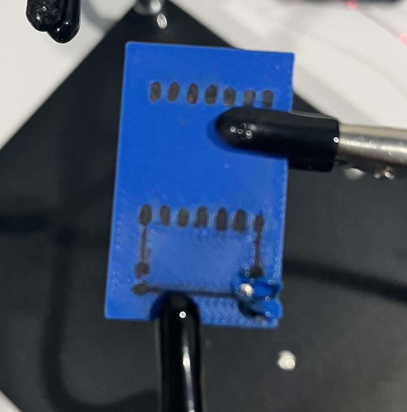
I did not mill the lightbulb on the pcb, because my toolpath ended up crossing my traces. This would have broken my circut. Instead I used the engraving tool my dad got me for Christmas last year, and drew it by hand. Thanks Dad!
When trying to attach the headers, I noticed the pins were very long. I cut them so that they would not cause a short.

I used soldering paste to attach the headers. I found both the heat gun and the iron to work well.

I must have touched the header with my soldering iron, it melted. I replaced it by heating the solder, and pulling the damaged header off the board.
this is why you should solder the small interier components first
This image also shows a mess of solder. I found that if the component fell over while hot, with solder on it, it was impossible to remove the solder from the copper areas.
You can also see the wires I used to jump over the traces in the board. There are 2 of them.

All soldered except for a switch, which I need to get.

I used the blink program I wrote earlier to test the board. I changed the pin to be GPIO4.

const int led = 4;
const int quick = 500;
const int slow = 3000;

void setup() {
  // put your setup code here, to run once:
  pinMode(led, OUTPUT);
  Serial.begin(9600); // Initialize Serial communication
}

void loop() {
  Serial.println("I have an idea!");
  // put your main code here, to run repeatedly:
  digitalWrite(led,HIGH);
  delay(slow);
  digitalWrite(led,LOW);
  delay(quick);
  digitalWrite(led,HIGH);
  delay(quick);
  digitalWrite(led,LOW);
  delay(quick);
}