Week 8:Electronics Production (PCB Rules)
Assignments
Group Work :
- Characterize the design rules for your in-house PCB production process.
- Submit a PCB design to a board house and document the workflow.
- Document your work to the group work page and reflect on your individual page what you learned
individual assignments:
Make and test a microcontroller development board that you designed
Group Work Assignment Reflection
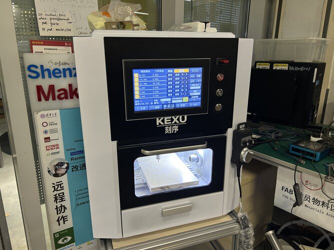
CNC Milling Machine Settings-KEXU(刻序)
- Touchscreen interface for control and monitoring
- Includes a small enclosed working chamber with internal lighting
- Equipped with a physical controller for manual adjustments
- Commonly used in industrial or educational makerspaces for engraving materials
Specifications:
- Working area: 190 mm (X) × 120 mm (Y) × 110 mm (Z)
- Spindle speed: 0–24,000 RPM
- Supported tool diameter: 1–6 mm
- Depth per pass: 0.1–0.3 mm
Copper FR4
Copper-clad FR4 is a widely used material for printed circuit board (PCB) fabrication.Properties:
Substrate: It's a thermoset plastic laminate made from woven fiberglass cloth bonded with an epoxy resin that is treated to be self-extinguishing.This creates a strong, rigid, and very good electrical insulator.
Copper-Clad Layer: This is a thin layer of copper foil that is laminated (bonded under heat and pressure) onto one side only.
Board Thickness: 1.5mm (standard thickness for many PVB applications)
40° V-Carbide Milling Bit
- Used for engraving fine PCB traces and cutting board edges
- The sharp angle allows for precise detail and narrow trace isolation
- Suitable for shallow cuts and high-precision milling tasks
- Suitable for shallow cuts and high-precision milling tasks
Individual Assignments
- Used for engraving fine PCB traces and cutting board edges
- The sharp angle allows for precise detail and narrow trace isolation
- Suitable for shallow cuts and high-precision milling tasks
- Suitable for shallow cuts and high-precision milling tasks
Individual Assignments
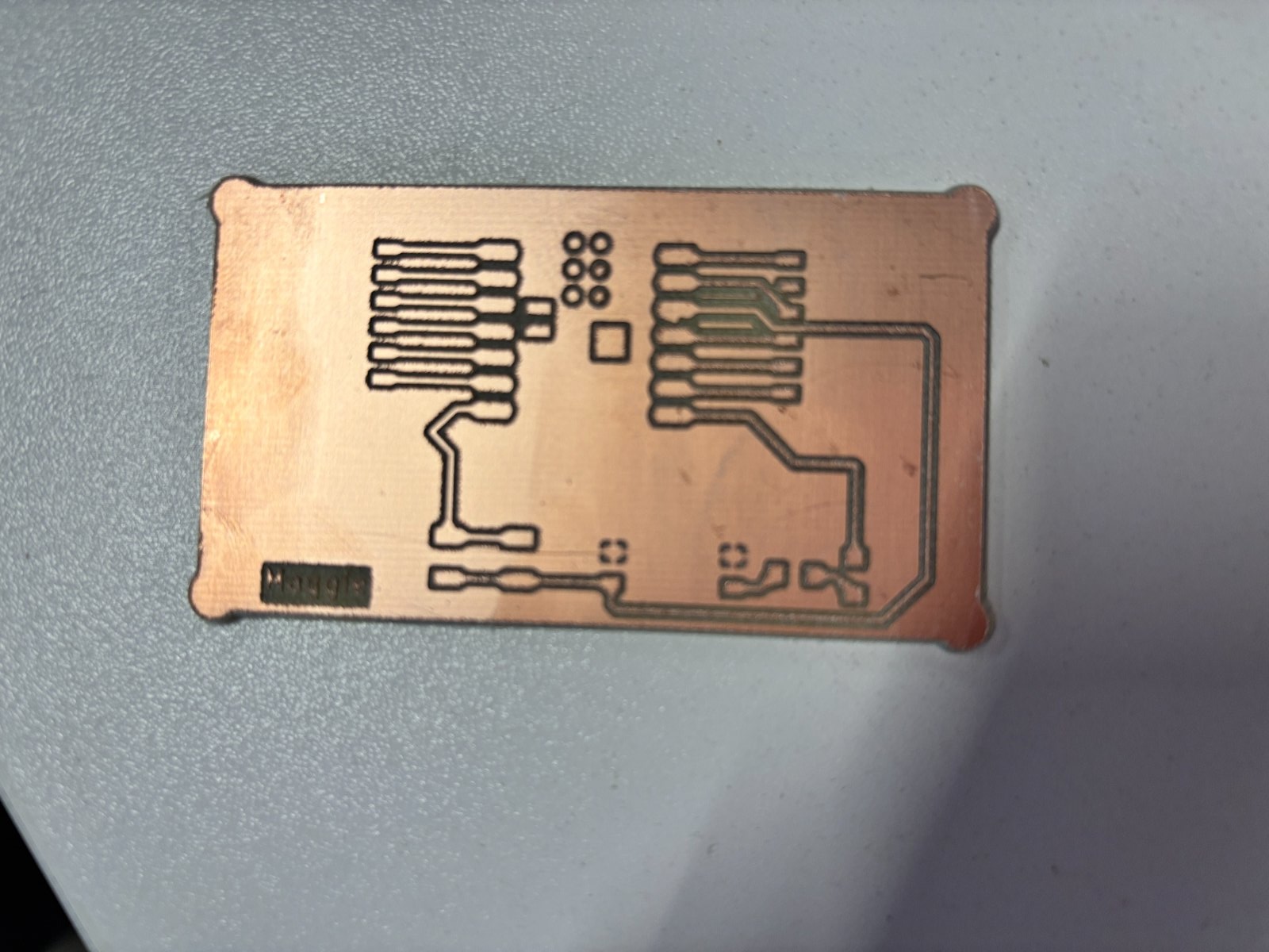
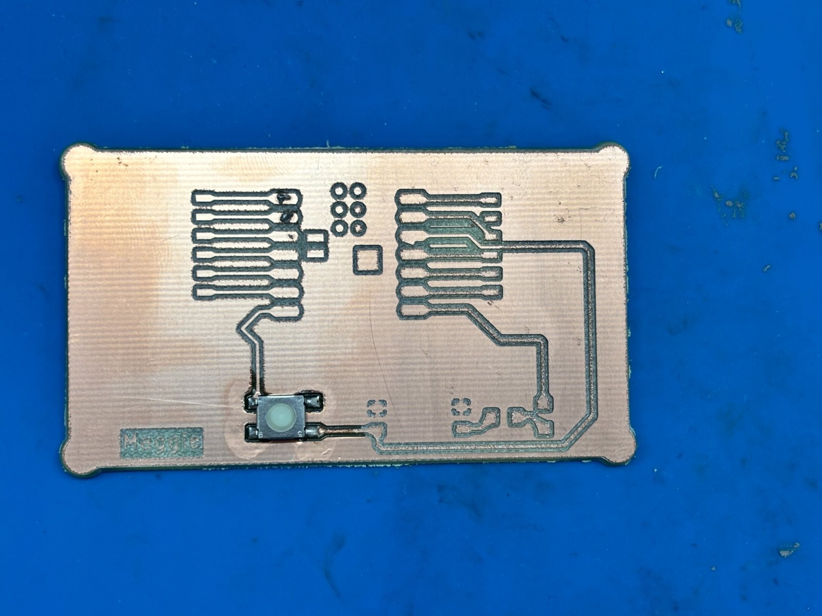
I had fininshed the PCB design on week 6, so firstly, I need to prepare the Gerber file from Kicad.
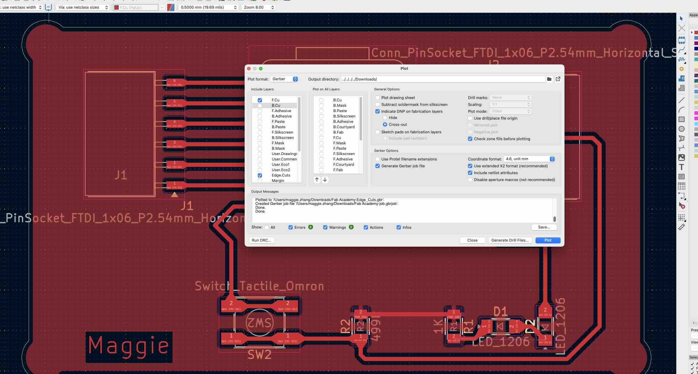
Go to File -> Fabrication Outputs -> Gerbers (.gbr)
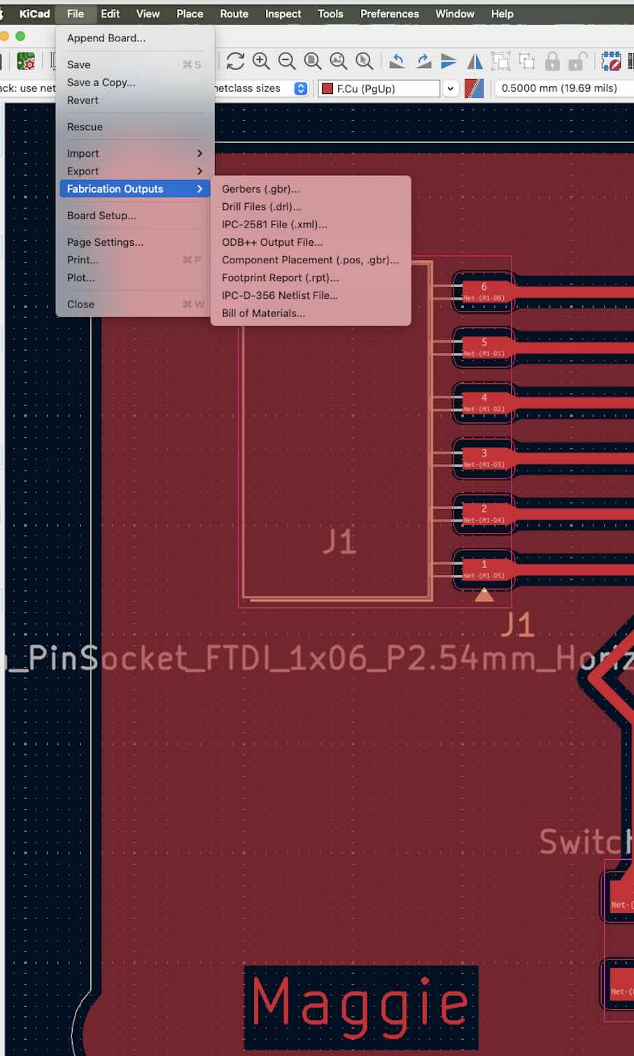
Select the layers that you want to export.After that the Gerber files will appear in the designated folder.
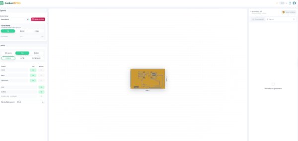
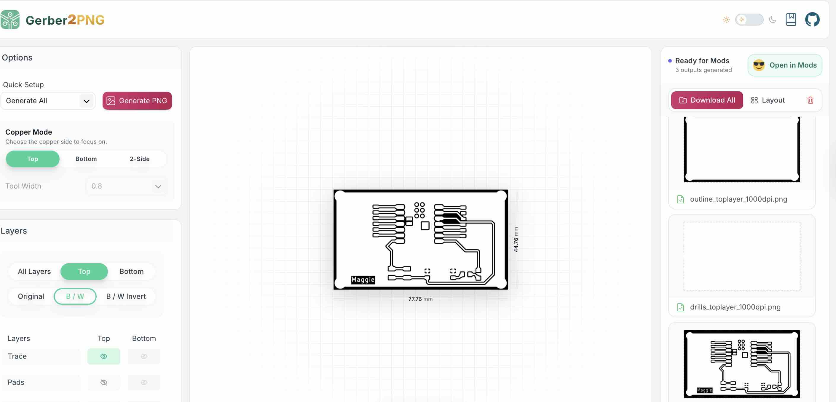
Next,convert the Gerber files to PNG files using Gerber2PNG
,make sure to upload the whole zip file not the single gerber file.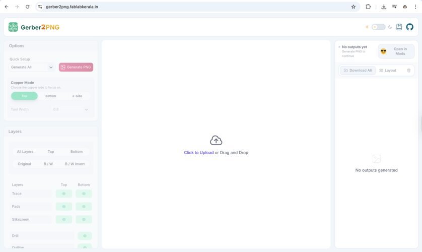
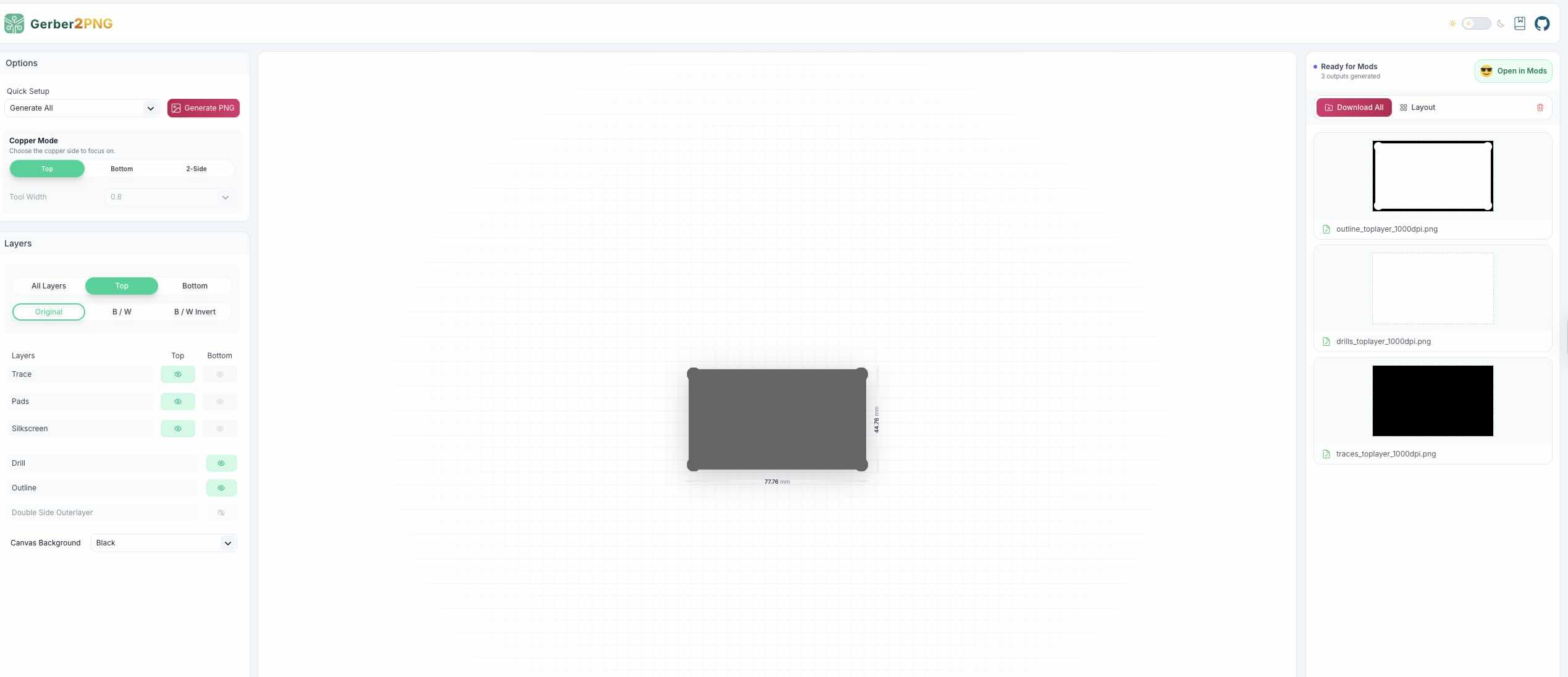
After generated the output files will appear on the right side of the screen,then you can download them separately including the outline file and the traces file.
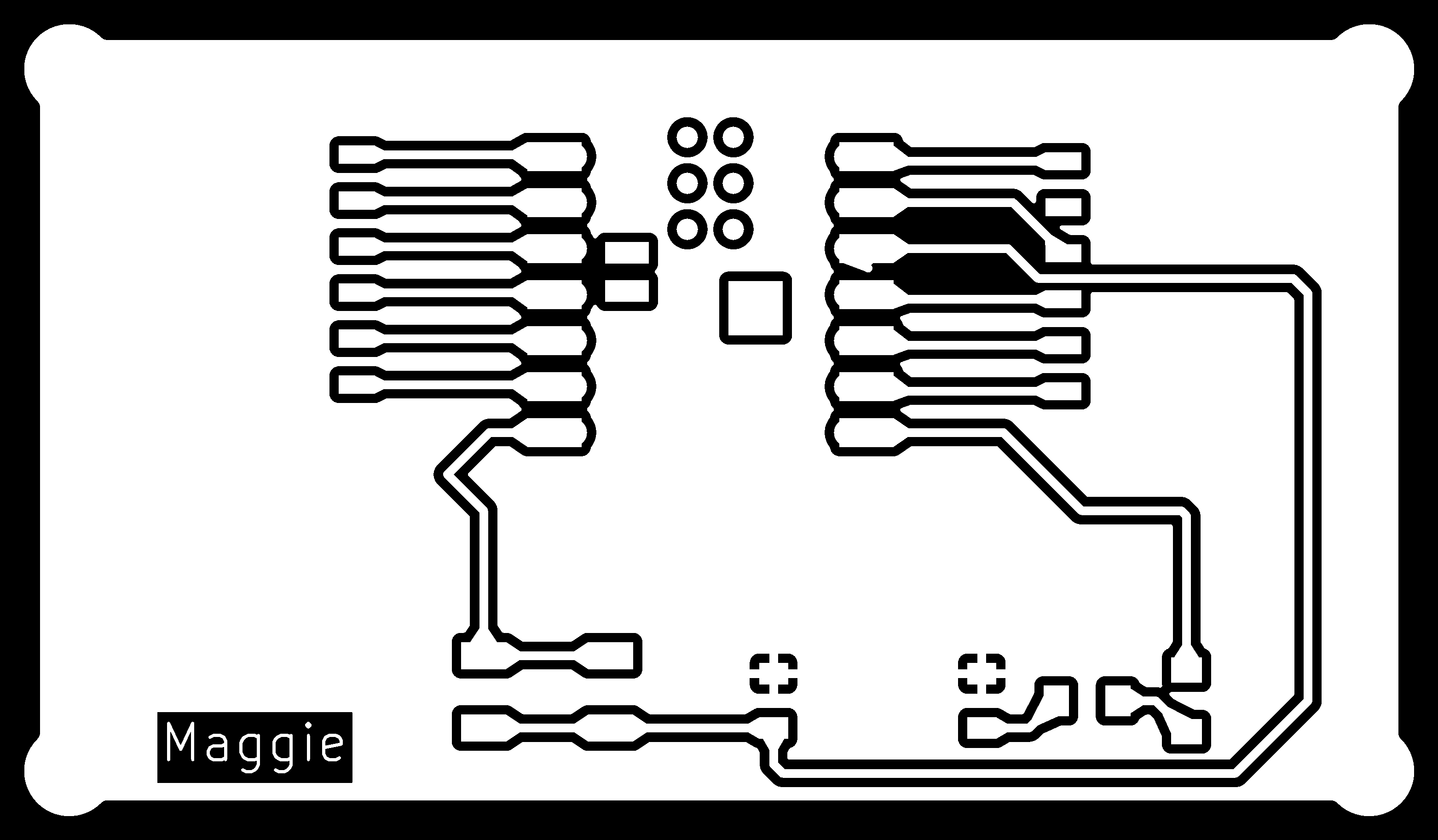
If the trace file is correct the traces should appear white, and the backgroud should be black. If you upload the single Gerber file, the trace file will not appear to black and white and cannot generated,only the outline file will appear.
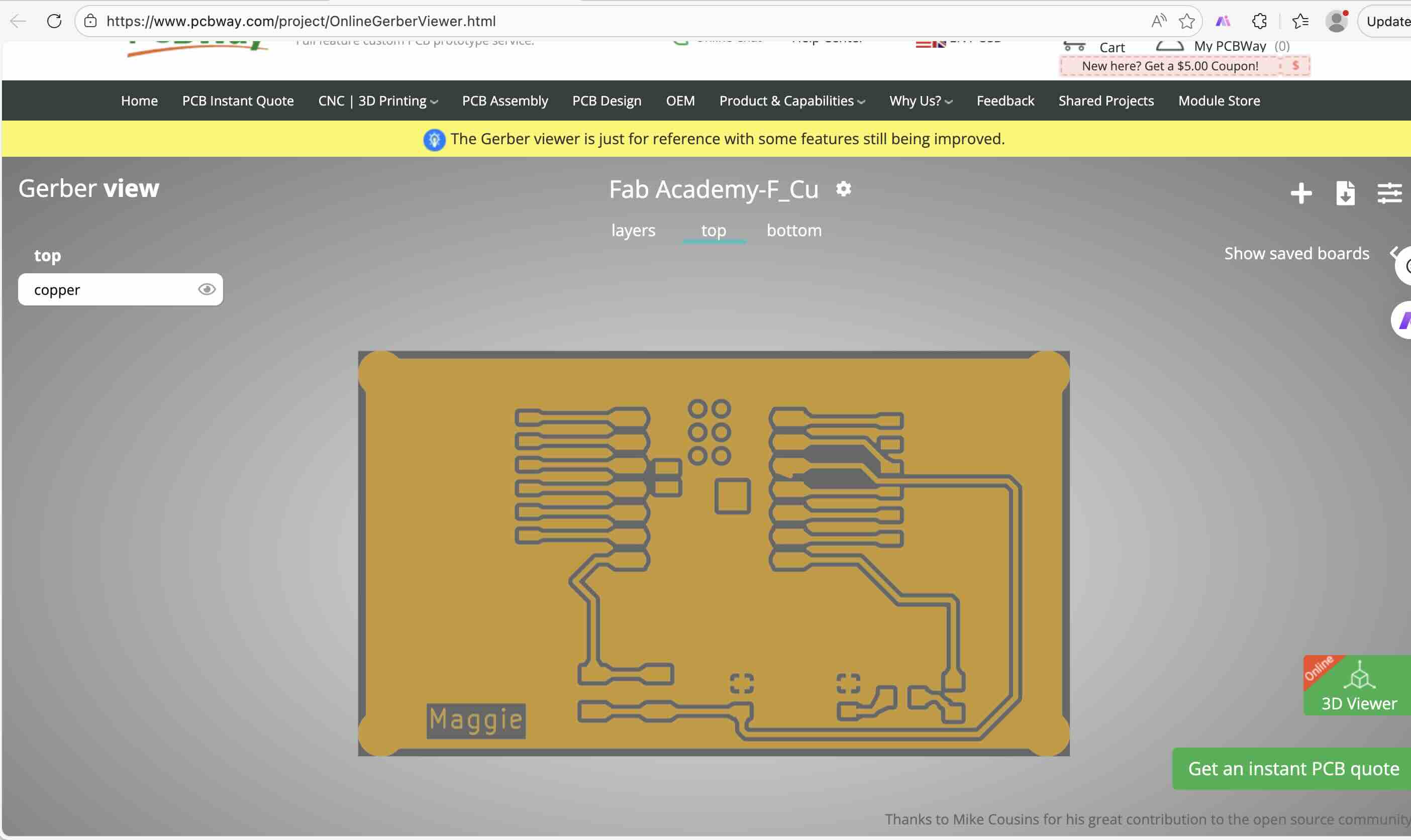
I also tried the other tool that canbe used to convert Gerber file into SVG file,GerbView

Next step, we should convert the PNG files to G-code file using Mods Project
Both files should be as the input for Mods.This tool works with both SVG (top section) and PNG (bottom section).
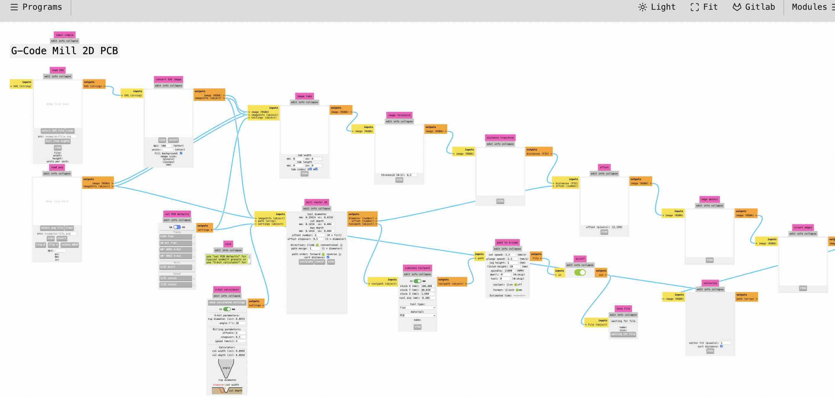
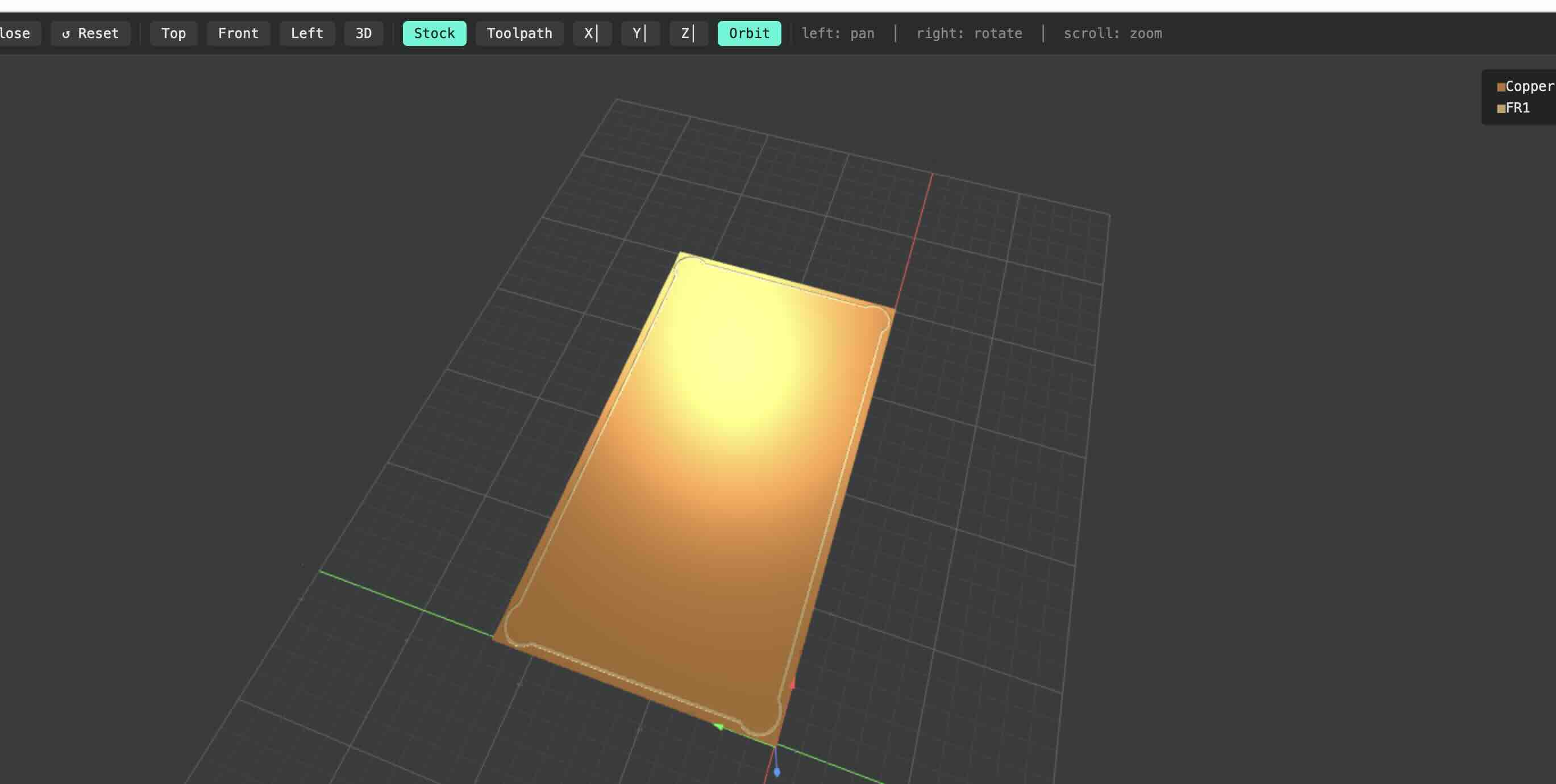
Select the outline png file, it will appear in the preview like this:
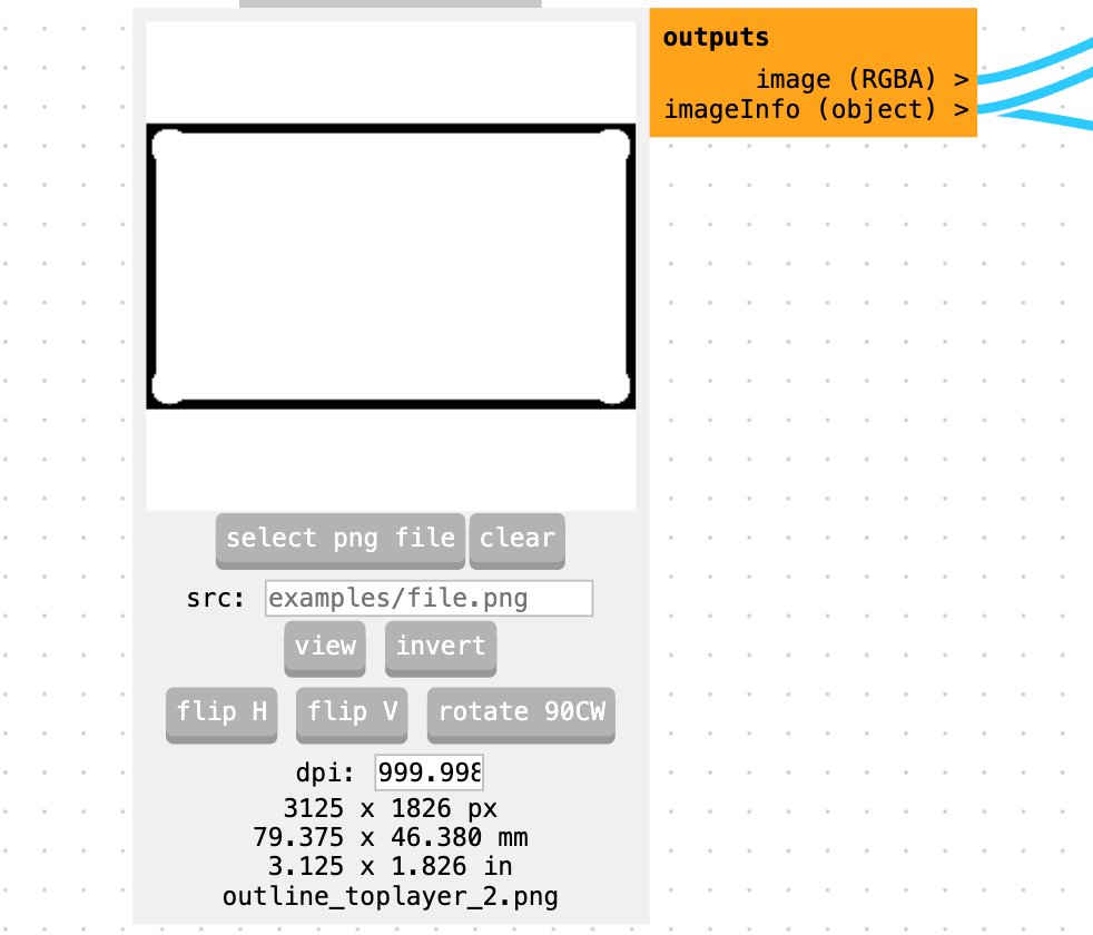
Set the PCB milling preset: Choose “40°#502 V-bit”
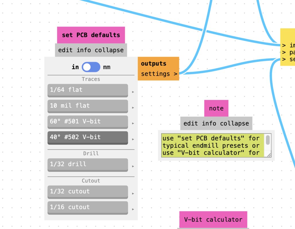
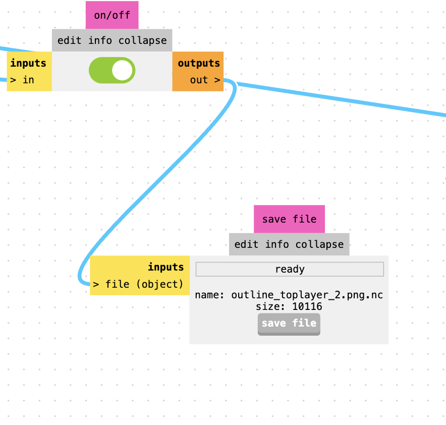
In Mill Raster 2D, click “calculate” to generate the G-code, then you can see the 3D view like below,then Click “save file” to download the G-code.
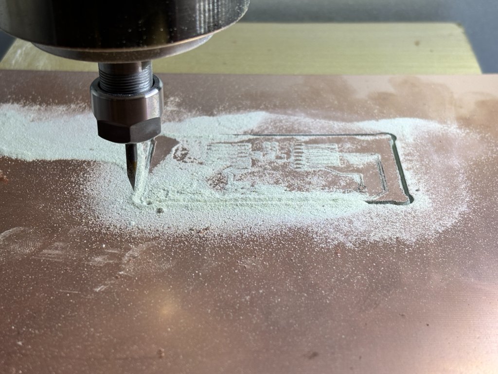
After prepareing the G-code file, we need to upload the file to the CNC machine and run the program.
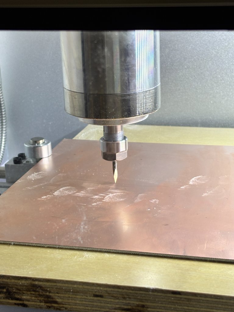
- Fix the copper plate onto the machine bed.
- The milling process will start from the bottom-left corner of the board, so we need to set the zero points for the tool.
- We can move the tool along the X, Y, and Z axes using this controller.
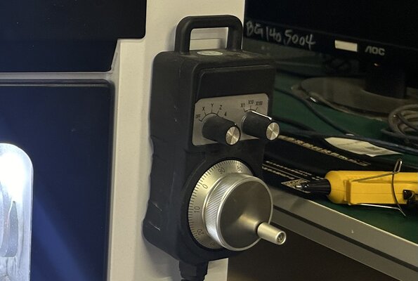
First, fix the copper plate onto the machine bed.
Then reset the coordinates to zero.
Since we manually moved the axes, the coordinates are no longer zero. Press “手动” (Manual) to display coordinates:
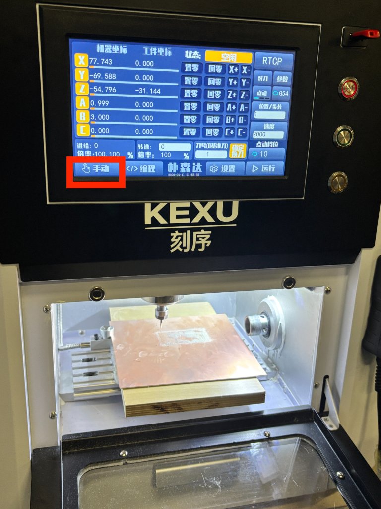
Press “置零” (Set Zero)then click confrim, repeat for X, Y, and Z until all values are zero:.
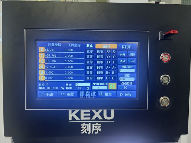
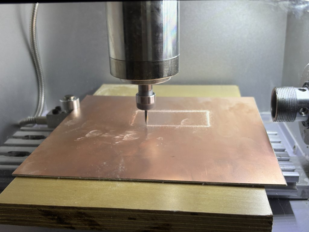
Select the file to start milling. Press “运行” (Run) to select the file, I chose the trace file first then change the dill for the outline file carving.
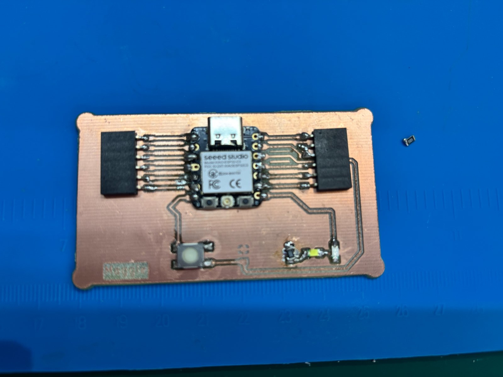
Assemble the PCB Board
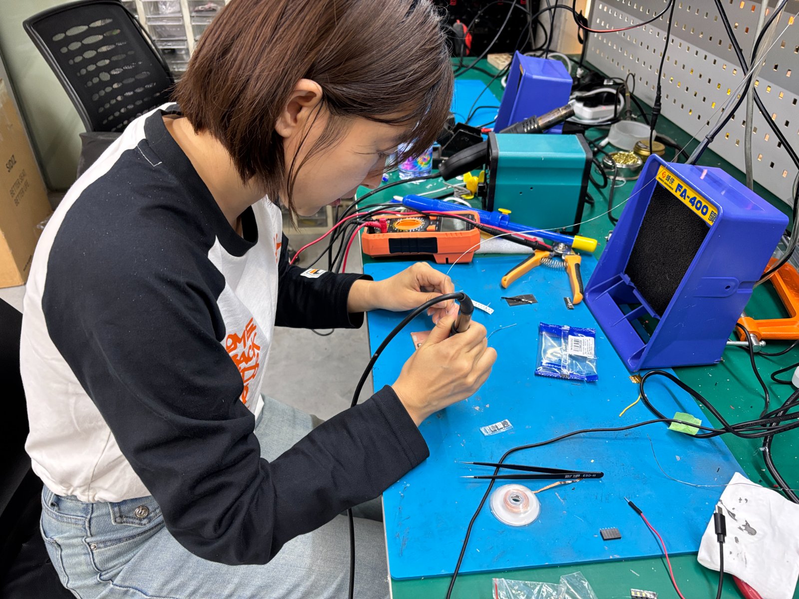
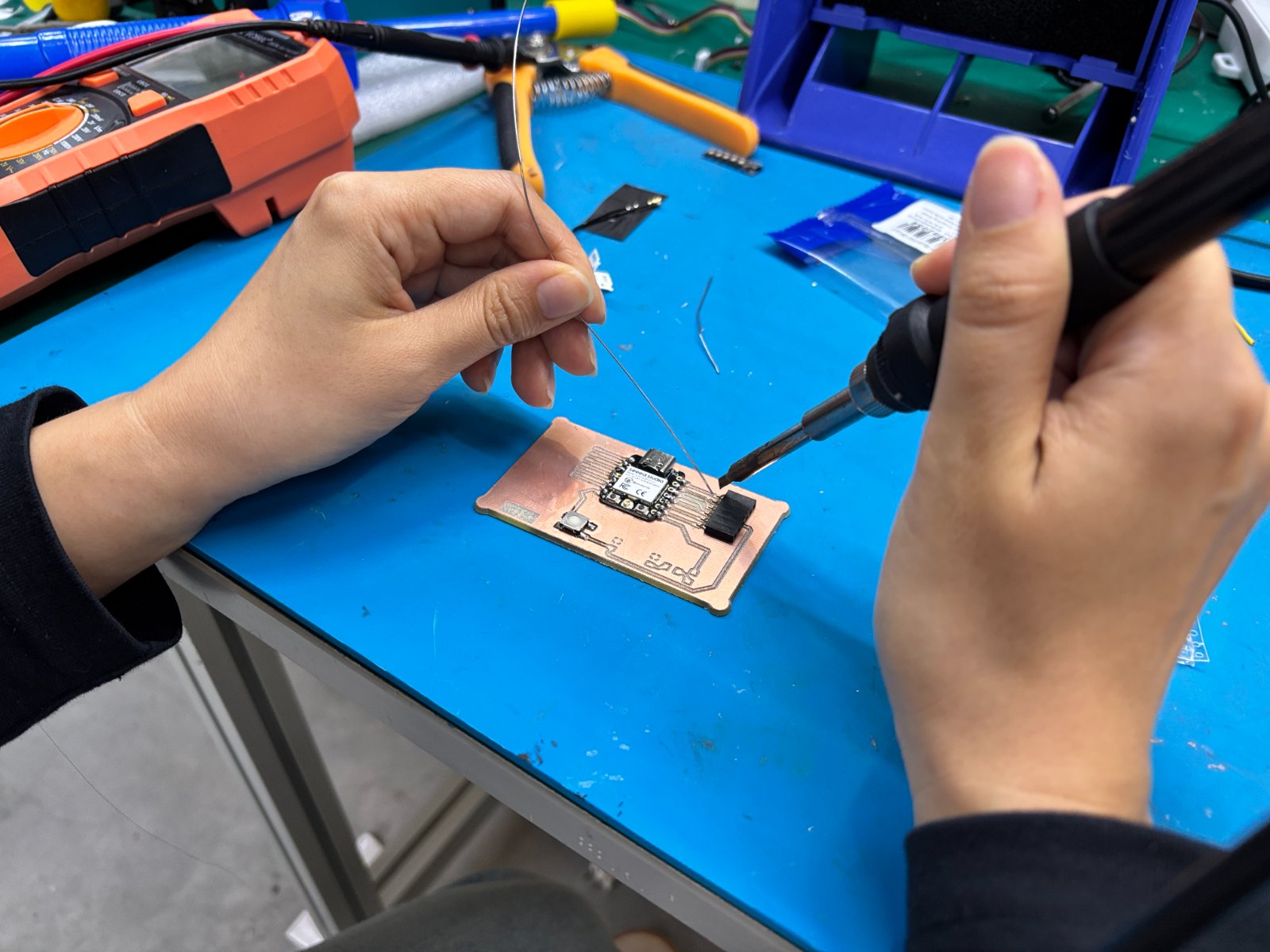
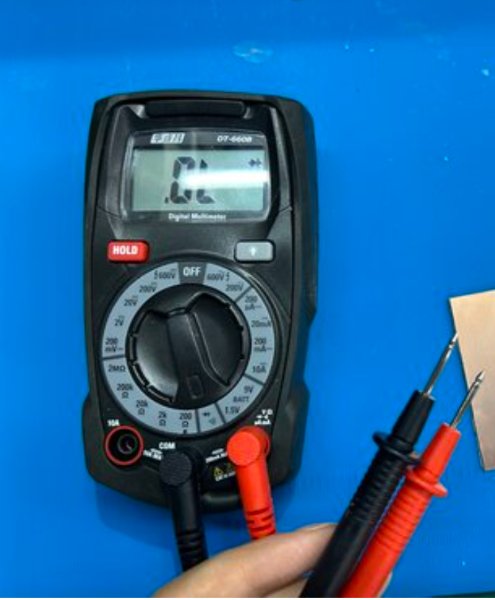
After milling the PCB board, we need to assemble the board using solder paste or solder wire, placed the components on the board and solder them together. After fninshing the buttons,leds,resistors and XiaoESP32, the PCB board is ready,but I need to test the board is working or not. So I Used a multimeter to check whether the circuit on the PCB is functioning properly and if there are any short circuits.
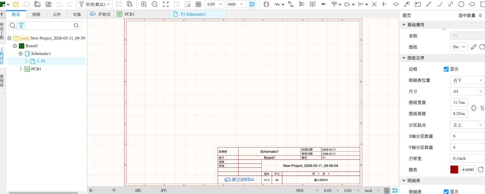
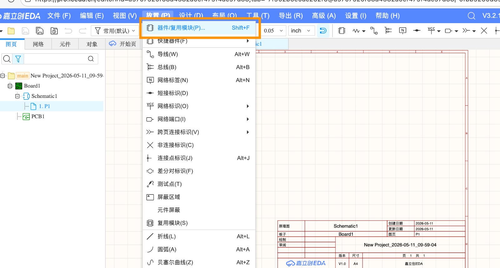
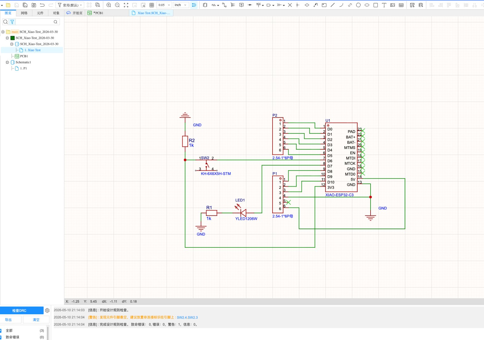
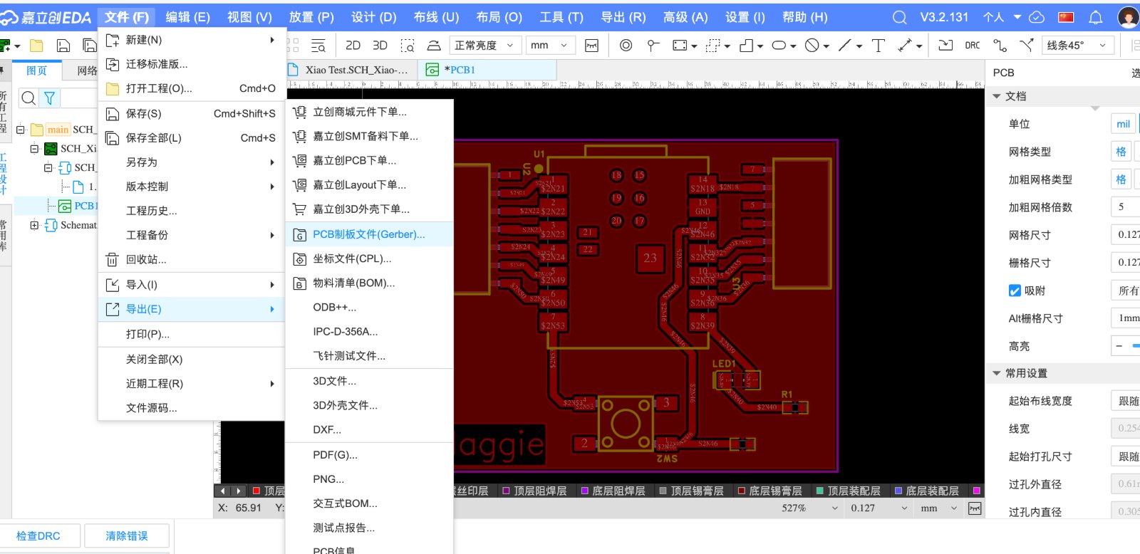
I also tried to use EasyEDA, to create a new PCB design and to convert the Gerber file to PNG file,to see the differences and the comments by using the Kicad and EasyEDA(嘉立创EDA). Because I'm worried my own will not working well, and I want to send to the factory to see the difference.
- First, Create a new project-Log in to EasyEDA, click "New Project", name it, and optionally add a description.
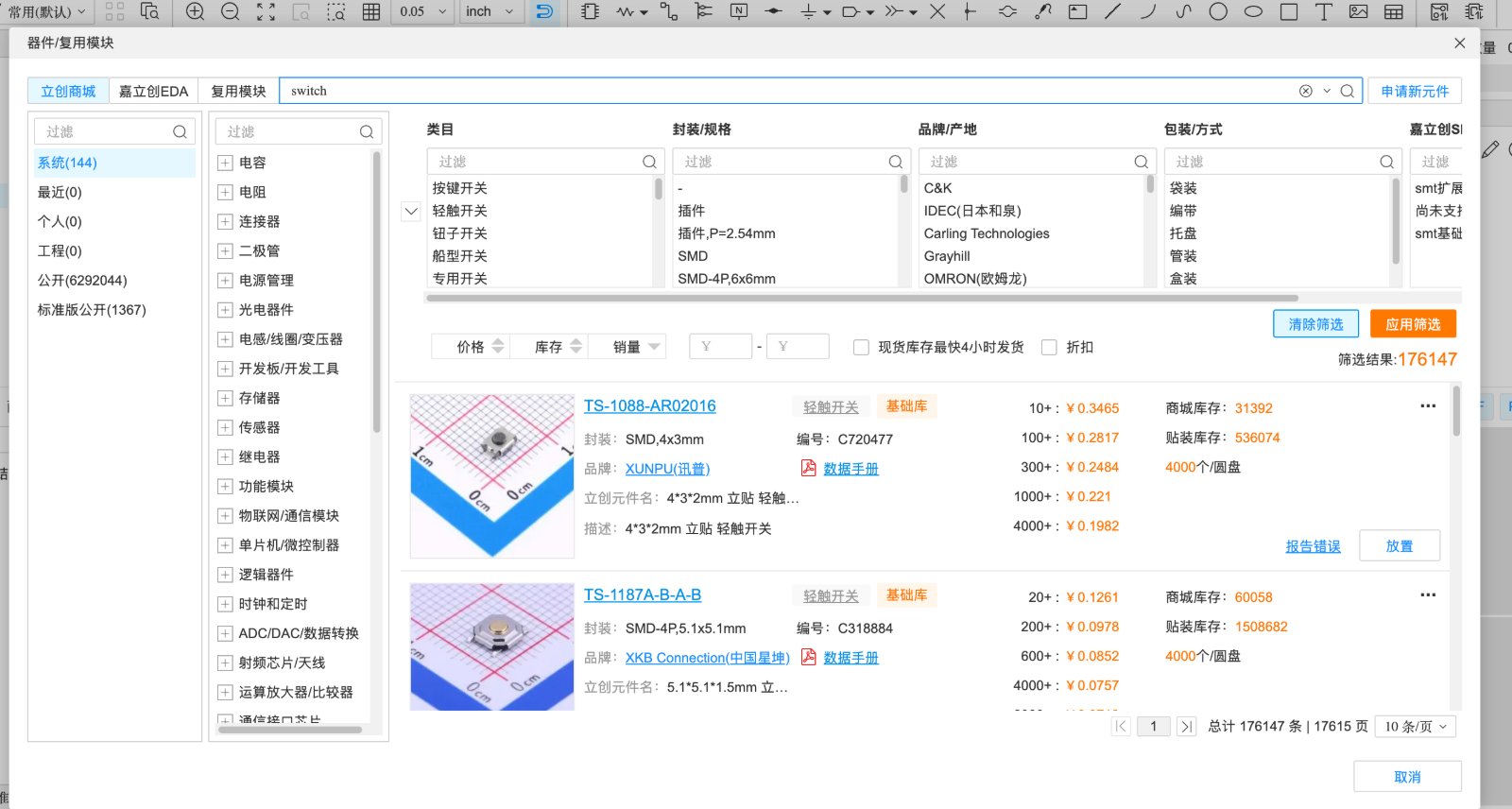
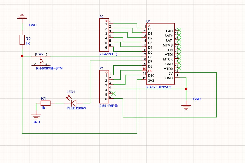
- Then, add the components you need to the project. You can search for the components you need in the library.
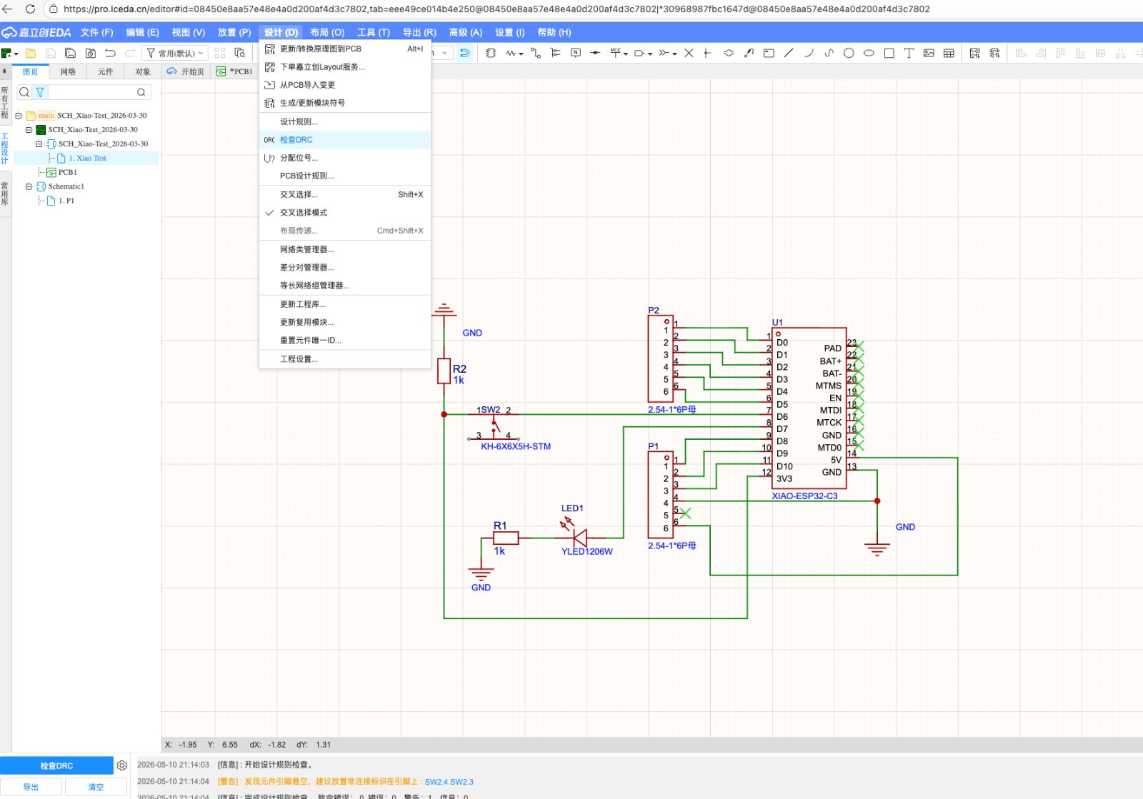
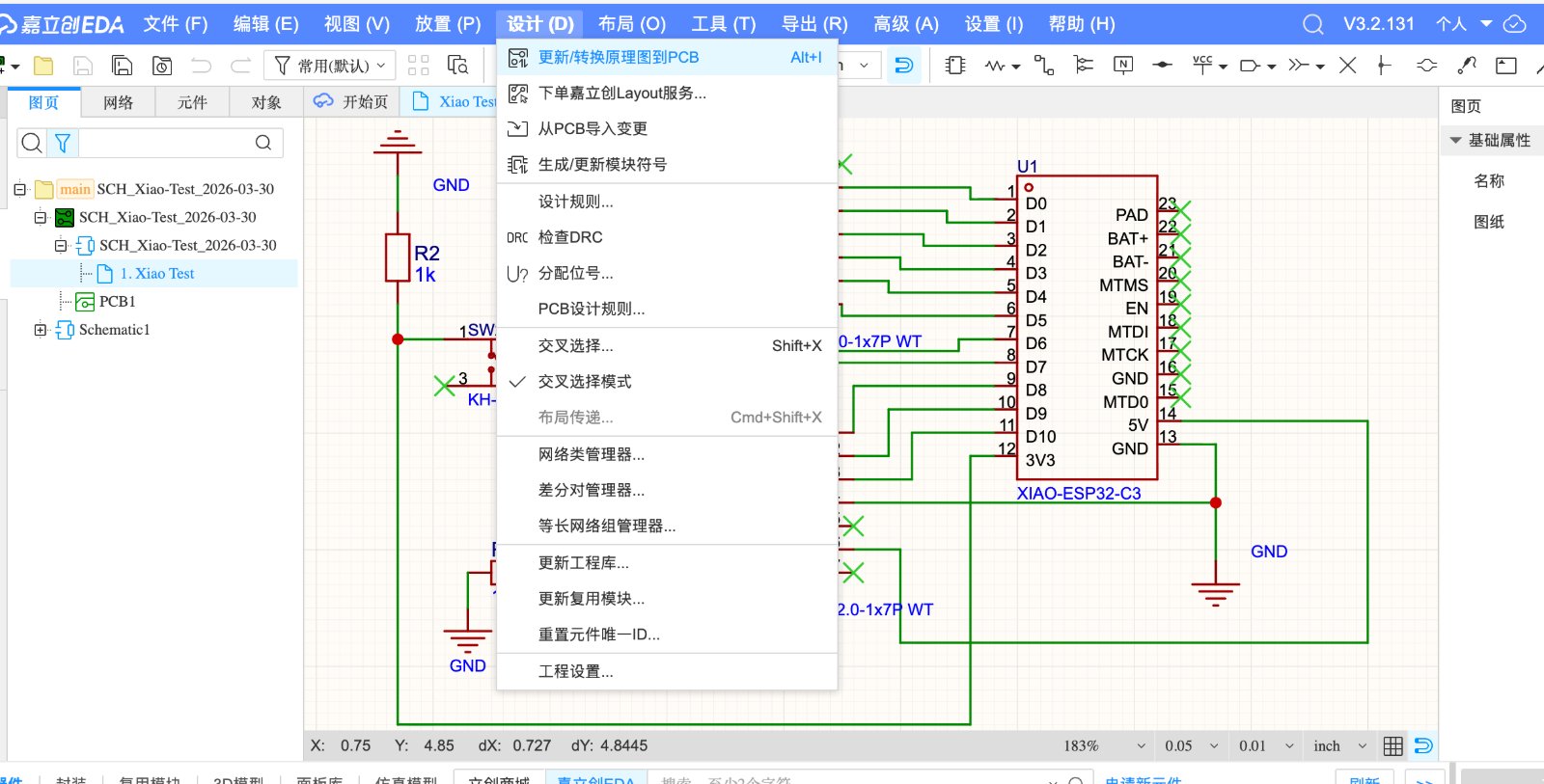
- Convert Schematic to PCB Layout – Go to Top Menu > Design > Convert to PCB. EasyEDA will transfer the components and nets to the PCB editor. Before conversion, verify all components have correct PCB footprints; missing ones will generate errors
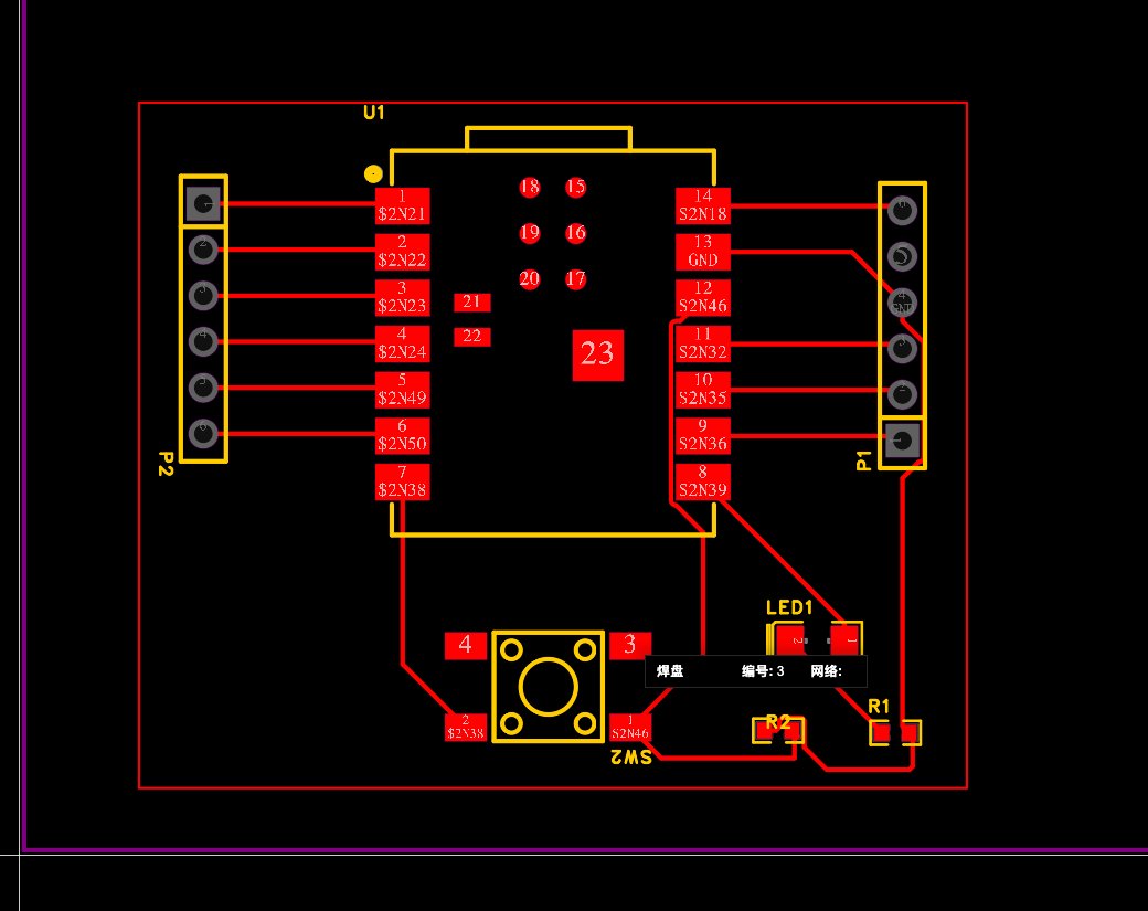
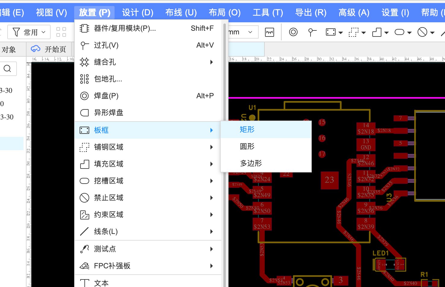
- Set Board Outline – Before placing components, define the physical board shape. Switch to the Board OutLine layer and draw using lines/arcs. For standard shapes (rectangular, circular, rounded rectangle), use Top Menu > Tools > Set Board Outline Wizard
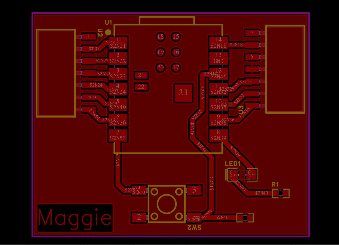
- Place Components – Arrange the transferred footprints inside the board outline. Group related parts together (minimize trace lengths) and consider mechanical mounting and connector placement constraints.
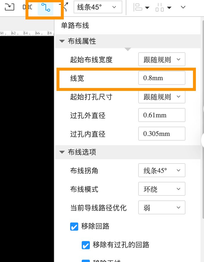
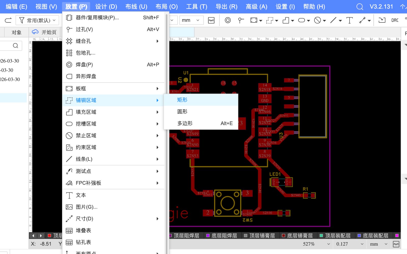
- Route the Traces – Use the routing tools (Track, Via) to create copper connections according to schematic nets.Remember to adjust trace width to 0.8mm
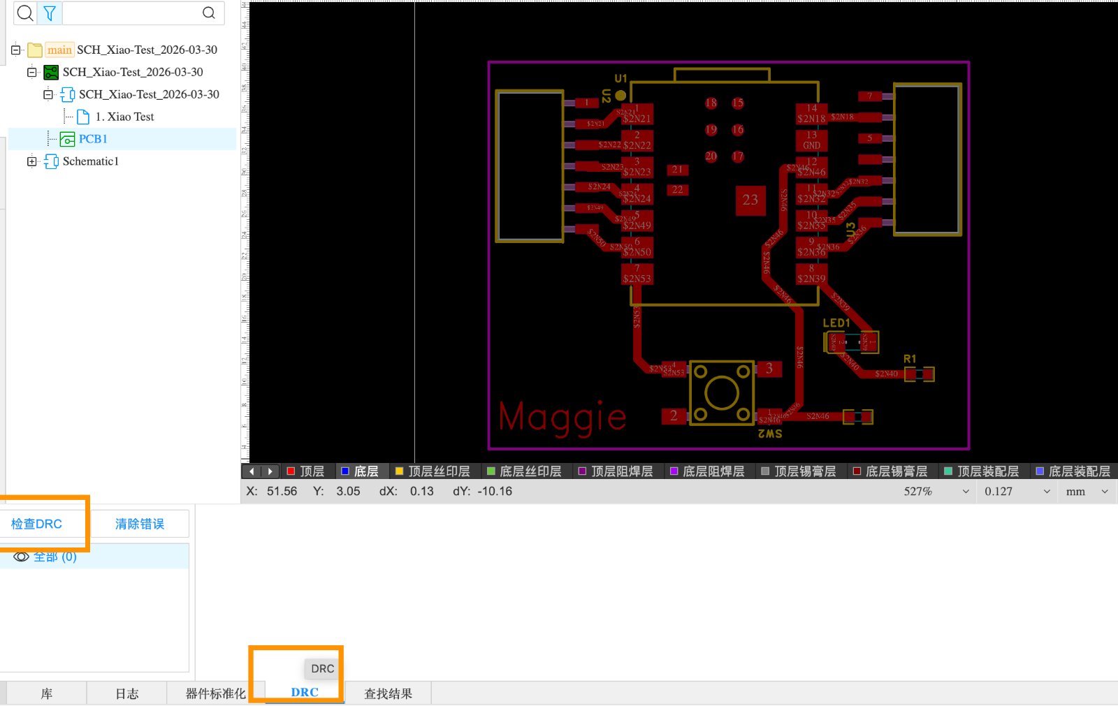
- Run Design Rule Check (DRC) – Before finalization, run Top Menu > Design > Design Rule Check to ensure no design rule violations exist and that the board is ready for manufacturing
- Generate Manufacturing Files & Gerber Files.
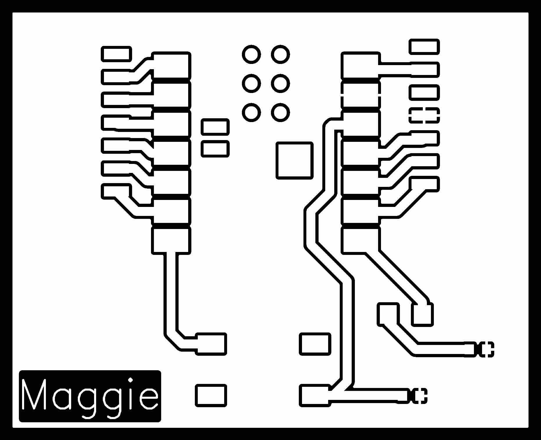
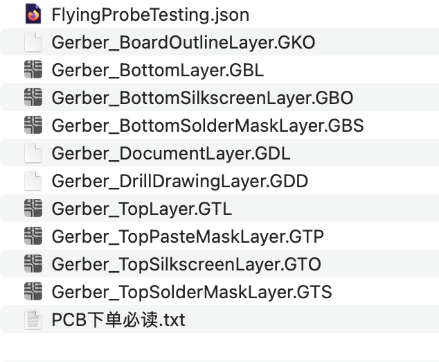
- At last using Gerber2PNG to convert the Gerber file to PNG file then download.But the difference is that EasyEDA will export a Zip file with the Gerber format, when import to the Gerber2PNG, you need to upload the whole zip file, instead of the single Gerber file. The unzip file looks like below:
Comparison between in-house milled board and the board from the factory
| Aspect | In-house milled board | Board house (factory) |
|---|---|---|
| Process | Subtractive CNC milling — copper is removed with a V-bit to isolate traces. | Chemical etching + plating in a professional PCB line (Gerber → manufacture). |
| Layers | Typically single-sided; double-sided is possible but alignment is harder. | Multi-layer boards (2, 4+ layers) with reliable layer registration. |
| Trace / feature size | Limited by bit diameter and mill resolution; wider traces and larger pads are safer. | Finer traces, smaller pads, tighter design rules (e.g. 6 mil / 0.15 mm and below). |
| Through holes & vias | No plated through holes — only top-side pads; wire jumpers or careful routing needed. | Plated through holes and vias; components can be soldered on both sides. |
| Solder mask & silkscreen | None — bare copper exposed; easier to bridge traces when soldering. | Green (or custom) solder mask and white silkscreen labels for assembly. |
| Surface finish | Rough edges, burrs possible; uneven trace depth depending on bed leveling. | Flat, uniform copper; HASL, ENIG, or other professional finishes. |
| Turnaround & cost | Same-day in the fab lab; material cost only (FR4 blank + bit wear). | Days to weeks shipping; low unit cost at volume, but minimum order and shipping fees. |
| Best for | Rapid prototypes, learning the full workflow, testing a design before ordering. | Final boards, SMD parts, repeatable builds, and designs that need vias or fine pitch. |
Gerber source file designed by EasyKAD: week8 Gerber File
Gerber source file designed by Kicad: week8 Gerber File