8. Electronics Production
This week we were given the opportunity to manufacture the circuit boards we had designed a few week ago. My big takeaway for this week is something that hadn't sunk in the few weeks before. I learned that the schematic is a plan, conceptual and symbolic giving information about how the circuit will function. One cannot expect that the same layout of wiring will be used in the PCB layout. Instead the PCB, is the physical resprentation of EXACTLY how the traces will be layed out, complete with location of the components and how the traces will connect with them.
Group Work: Characterizing PCB Production @ Wheaton Fab Lab
Examining a Test Board
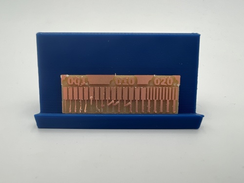
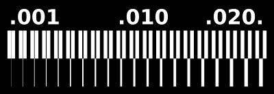
In groups we examined a test a board as pictured above. From the photo it is evident that the size of the traces in terms of width is incredibly important. If the traces are too close together the board will not function properly and there is also a risk of accidently soldering two traces or components together which should not be connected. The thicker the trace the better chance it would have to conduct current and most importantly remain affixed to the FR1 copper board without lifting. The cut off seems to be about 0.16 where anything small than that measured in mm would lift off the board. See Design rules section for mitigating these types of problems.
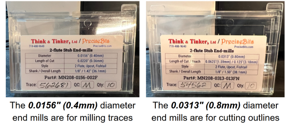
Our Machine and Endmills
The Machine we have in our lab is the Roland SRM-20. This is important to note as we will need to select this machine in the mods project interface in order to create cutting files that will work with our machine. We will be able to calibrate the x, y, and z axes on our machine using software called V-Panel.
There are two different size end mills we will use which will influence the size of the traces and the amount of spaces between traces. This is particularly important for moving current across the circuit uninterrupted and without a short. We ended up using 0.0313" (0.8mm) for the edge cuts and 0.0156" (0.4mm) for the traces of the development board.
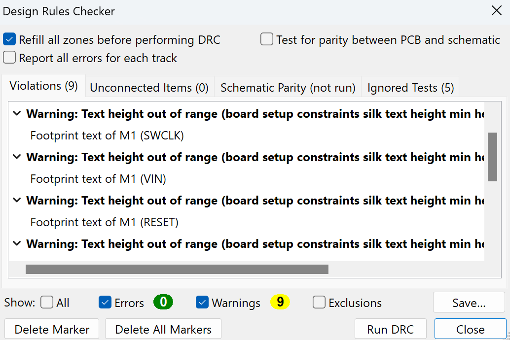
Design Rules Checker
In the Design Rules/Constraints menu I changed minimum clearance, copper to hole clearance, default clearance, and default track width to 0.44mm. Once those were set it only allowed me draw wires in PCB mode that our specific machine could mill based on kerf. That way I wouldn't end up with traces that were too close together but were thick enough to form good connections. Any time that I needed to edit the drawing in PCB mode I was able to run the DRC feature again to make sure that the board could actually be cut and had no errors. Design Rules checker can be found on the Board Set Up Tab on the File Menu.

Useful Files & Links
- Data Sheet for RP2040
- Tactile Button Data Sheet
- Moving KiCad to Mods & Roland Mill Tutorial
- Mods Project Website
Design Rule Warnings
I changed the design rules to align with the values documented above. Regardless when running the inspection I still received warnings but all warning had to do with the text height and after reviewing the warnings my instructor encouraged me to continue as this text would not be include in the footprint of the milled final project. Below in the picture is a sample of the text warnings.
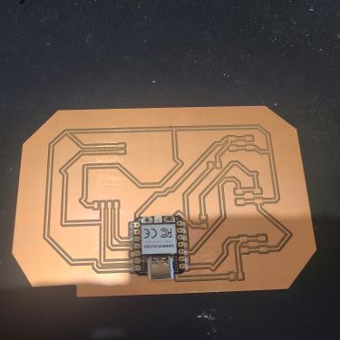
Development Board Design (Schematic and PCB Layout)
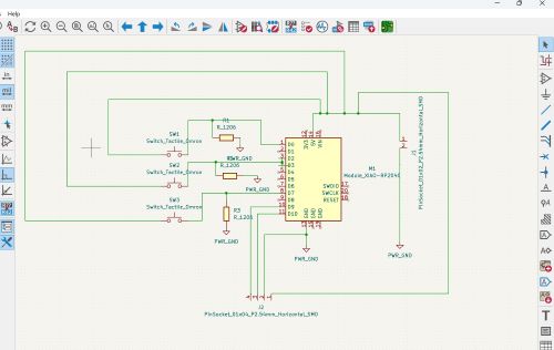
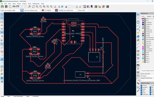
I first started by making an update to board design for an issue that was not caught by the KiCad inspection in PCB mode. I did not realize that each 10k Ohm resistor would need its own dedicated trace, so I went ahead and added a dedicated trace for each resistor going from each of the 3 buttons through its own resistor and then out to ground on the Xiao rp2040 chip. I had to make this change both on the schematic drawing in KiCad and then update the PCB sketch to reflect those changes as well. Something I had overlooked in previous weeks was making sure to add components, grounds, resistors, etc from the KiCad library that actually have footprints in the footprints library. When you click on the components to add a footprint image is generated for those components which have footprints in the library. To avoid issues when moving into PCB mode making sure you have the correct footprints or a footprint in general for each component is key! For my design I am using the Xiao RP2040, 3 tactile buttons, one 4 pin SMD socket, and one 3 pin SMD socket. The final board design after receiving feedback is pictured above.
Development Board Plotting
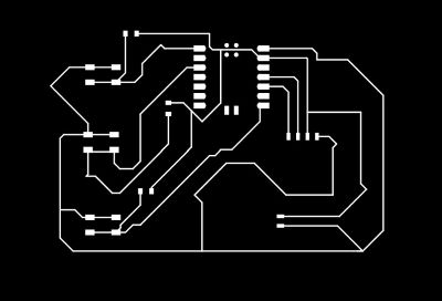
On the file menu I clicked on plots and in the layers menu I ticked the boxes for F.CU and edgecuts to specify the traces from PCB and the final shape of the board. I also ticked the box for negative plot and selected "generate drill files." This created two SVG files, one of the outline shape of the board and one of the traces. Both with black background and sketched in white as pictured below on the traces photo. The black and white photos display lots of white space in the background when the files are opened so the files need to be altered to exclude the surrounding white space in Adobe Illustrator and converted to .png files to be used in MODS. The goal is to combine the two files into one but as separate layers that can be milled by the machine in two different steps. The steps that I used for layering can be found in the Moving KiCad to Mods file in the useful links listed at the top of this page.
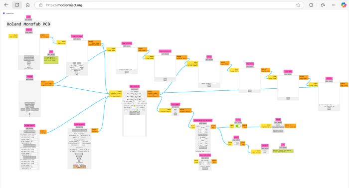
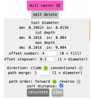
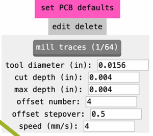
Using MODS Web Application
We used the MODS web application to create two RML files that could be read by Roland Machine. The mods applcation, as seen in the picture below allows you to upload the png files for both the traces and outline for the development board to the web application. There is also a module for the milling machine where I was able to adjust the speed to 10, and the x, y , and z axes to 0. See pictures below for additional module settings. When all the settings have been adjusted and you've uploaded your png you can click calculate and this will generate a tool path file for your traces. You follow the same process over again to create an RML file for your outline however in the PCB defaults module be sure to click mill outline (1/32)
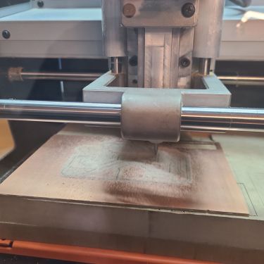
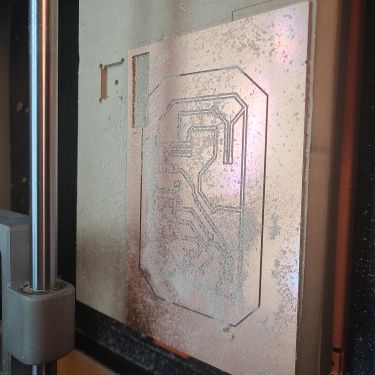
Milling the Board on the Roland SRM-20 Milling Machine
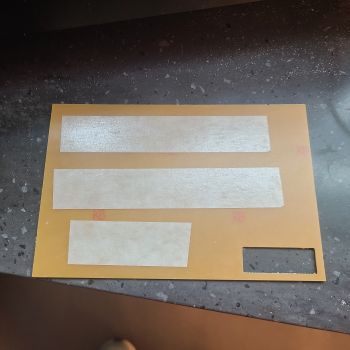
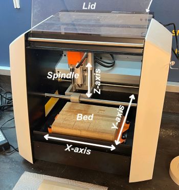
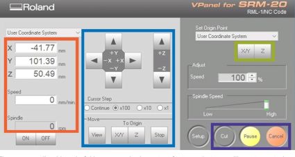
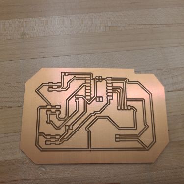
To mill our boards we used FR1 Copper Clad that was single sided. The board would be milled with the shiny side up and we needed to use several pieces of strong double sided tape to affix the board to the bed. See pictures below of the machine and double sided tape. I first had to load the end mill with the correct size to mill the traces first. The traces required 0.4mm end mill while the outside edge cuts required 0.8mm. The end mill can be added by losening the collet with a allen key and placing the end mill bit into the neck of the collet and then tighten. Next I had to check the height of the end mill while setting the X,Y, and Z origins. This can be done by using the x an y buttons on VPanel to move the end mill to the front/bottom/left corner of the copper clad. I lowered the Z on Panel to adjust the endmill and then set the X, Y, and Z origins. Next I raised the Z axis to pull the endmill away from the board by at least 5mm. I then clicked "cut" and chose my RML file for the traces file and added it to VPanel and then clicked output for the machine to begin cutting. When the traces were done cutting I opened the machine to vacuum, removed all the dust, and checked that the traces had cut properly. I then repeated the steps with the RML file for the edgecuts. But first I had to change the end mill again by removing the 0.44mm bit and replacing it with the 0.8mm bit that would be used to do a clean cut around the shape of the development board. When the edgecuts are complete, it is best to remove the development board and any scrap copper with a metal spatula. Then remove the double sided tape and check for any loose or unsmooth edges around the traces. Any rough spots can be lightly filed away using damp sandpaper.
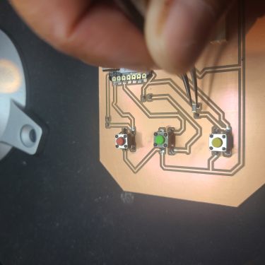
Soldering the Components and Power Test
I used the soldering station in our fab lab to do two different types of soldering. The station has a soldering iron, a hot air nozzle, lighting, magnifying glass, and a fan to pull fumes away from the work space. I used soldering paste for the rp2040 chip and for the resistors. The paste has to be applied to the copper pads and then blown by hot air at more than 700 degrees. The connections are secure when the soldering paste has turned to a shiny silver surface. The resistors are quite tiny so I used the special lighting and magnifying glass in addition to tweezers to place each resistor. They are really much too small to handle with bare hands. I used a soldering iron to add extra soldering material to the chip and also used this method to secure the 3 buttons as well as the SMD pin sockets. The method requires using the soldering iron which is shaped like a pen to heat the tip of the soldering wire and allowing the melted material to fuse itself to the copper on the board and metal on the connectors for each component. I was able to use something called a soldering wick to absorb melted soldering material in the areas where I had applied too much.
Testing
The initial power test for the chip was a failure. When it was first plugged in to the usb power the rp2040 itself never lit up but instead made a crackle and then a popping noise which was followed by an odor which made believe that something had certainly burned. The chip then began to become incredibly hot so I disconnected the chip.
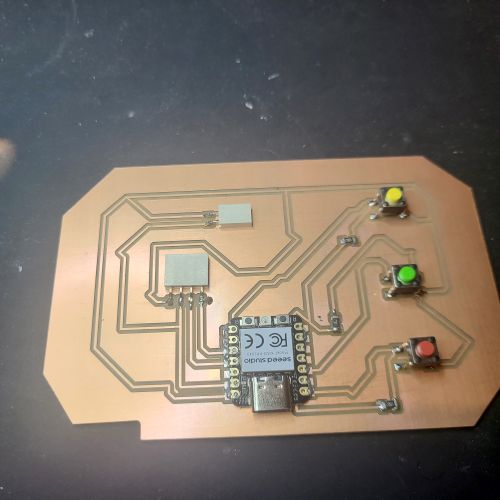
I decided to cut a new board since the first one smelled strongly of burnt electronics and one of the sockets on the 4 pin SMD socket was melted. I repeated the milling steps above since I was able to use the same files. I was extra careful to solder more neatly than last time to avoid the same problem again. This one powered up just fine when powered by USB as can be seen in the video below.
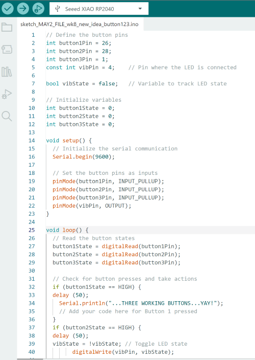
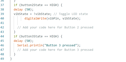
I was able to find code by googling "code for 3 button dev board with arduino ide". It brought me to the SEEED Wiki page. I of course had to alter the code to suit my needs as the original code was simply organized to send a message saying Button #x pressed for each of the 3 buttons when pressed. I changed it so that the yellow button gave an output of "button #3 pressed." When I pressed the blue button it turned on the ERM button motor. When I pressed the black button, it turned off the motor and displayed a message about there being 3 working buttons. The video is below.
Here are the screenshots of the final code used and the video:
Design Files for this Week
KiCad File for Development Board PCB KiCad Schematic File Plots for Edge Cuts svg Plots for Traces svg RML file for traces RML File for Edge Cuts Arduino IDE code to test 3 buttons