6. Electronics Design
This week we began to study electronic circuit board design, of course with the intention of soon building the boards we would design for this week's work. We also began working with a new software called KiCad which allows you to first map out your circuit board design with componenents, wires, and resistors. It then allows you to design and alter the shape of the final board and circuits in it's PCB design interface. I will share additional information on that below.
Measuring Voltage with the Oscilloscope and Digital Multimeter
In addition to exploring design, we also began to explore electronic components and equipment for measuring voltage in our lab. Specifically we learned to use two different types of equipment: the Digital Multimieter and the Oscilloscope. Both can be used to measure electronical currents, power in voltage, and for diagnosis and debugging electrical circuits. In our lab we tested batteries and LED bulbs using the microcontrollers we were most familiar with you can see our group assignment results by following this link here: Group Assignment
Introduction to the KiCad Software
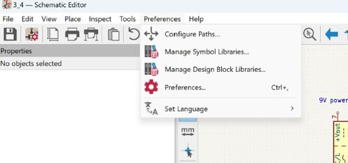
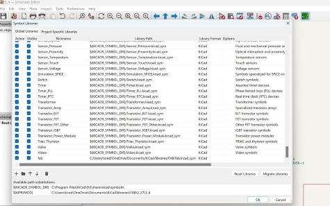
I downloaded version 9 of Kicad by visiting the following link: KiCad.Org In addition to downloading the software we also needed to dowload the Fab Academy's library of parts in terms of symbols and footprints. One can visit the preferences on the top menu and on the drop down click on manage librarys. One bit of advice here is to make sure that you pay attention to capitalization or more important lack of when typing the name of the target folder to receive the library files, otherwise your destination folder will end up empty. Having access to the libraries will allow you to add components from the fab academy library in and when in PCB editing mode the library will also supply footprints for mapout what your final circuit board design will look like. There are also additional libraries available through Digikey.
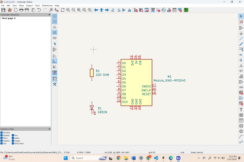
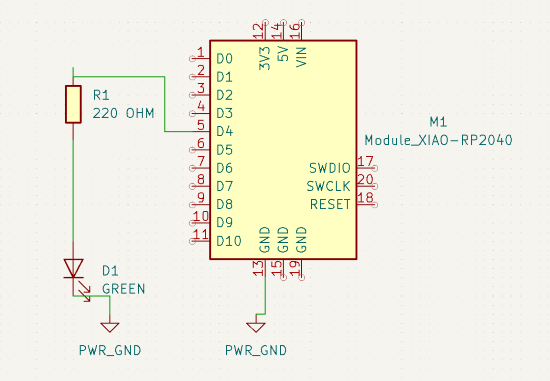
We took a look at the RP2040 microntroller on KiCad which allowed us first to begin in the schematic design screen. Here you can add components, wires, resistors, etc by clicking on "add symbols." You can add anything that is in your library but it is of course recommended that you choose components and pieces that have an actual matching footprint in the library. If there is no footprint in the library you will not be able to add that component in the PCB Design screen. Each component in the library has a description and a datasheet where more information can be found. It also lets you know if indeed there is a footprint for that component. Once you choose all your components, in this case an LED, the RP2040, and ground wires, and a resistor; you can drag and arrange the components how you'd like. Then add wire by clicking on the straight line icon that says "draw wires." Below you can see the schematic with and without wires.
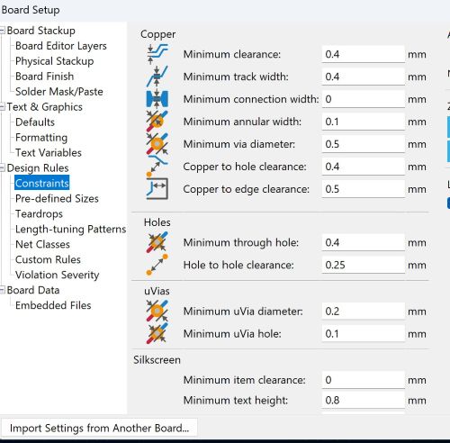
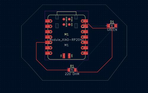
You can enter the PCB Mode by clicking on the green icon that looks like a microchip at the top of the menu. If your pieces don't copy over immediately, visit the top menu for tools and then click update pcb from schematic. From there you can add wires as I described above, similar to the menus in schematic mode. However, when in pcb mode you will need to choose a shape for your final chip once you have checked it for errors by clicking on inspect. It is key that you adjust the setting to match your labs equipment. For instance in our lab we need to adjust the board minimum track width to 0.4 as that is the smallest width our machine can work with without printing the circuit board incorrectly. These setting can be changed if you click file and then Board Setup. See the picture below. On a final note you can also sketch your circuit boards final shape by clicking on the right side menu and choosing "edge cuts". This will allow you to put lines or a shape around your board.
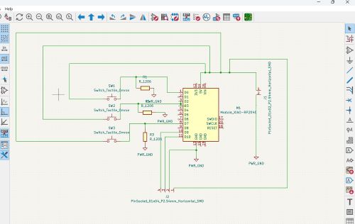
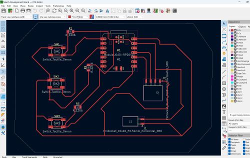
My Development Board
Our assignment for this week was to use an EDA tool to design a development board that uses parts from the inventory to interact and communicate with an embedded microcontroller. I of course continued to use KiCad and the microcontroller I chose was the Xiao RP2040. I am hoping to use this microcontroller as part of my final project and I believe the design of this board will move me into the direction I plan to go with the project in the end. With the RP2040 I also added 3 tactile buttons, a 2 pin SMD socket and 4 pin SMD socket. I have seen some output devices that have 2 wires and others that I have more so I believe this will be a great place to start. I hope to program the buttons later to control a 2 wire ERM motor or a mini vibrating motor for a specific length of time. I was able to find all the symbols and footprints in the fab academy library on KiCad. I chose each item from the library and dragged and dropped them onto the schematic worksheet. I then added ground symbols and resistors. I then added all the wires to the schematic drawing followed by a shape enclosure which gives the final shape of the circuit board in the same way that I completed the one above by using the cut edges feature on the right side menu. I am hoping to program a certain amount of time to lapse for the vibration to start and stop.
