
About this week
This week, we learned about circuit design, including how to use software to design and finalize PCBs. We worked with schematic and PCB editors to design circuits and then turned those designs into a finished printed circuit board (PCB). This process involved drawing the schematic, placing components, connecting the traces, and making sure the design is ready for manufacturing. It gave us practical experience in turning a design into a real, working product.
Objctive of the Assignment
1.Gropu Assignment -
2. Indivisual Assignment -
About Electronic design
Electronic design is an intricate process where various electronic components, such as transistors, resistors, capacitors, and other devices, are carefully selected and integrated to achieve a specific purpose, resulting in a functional circuit or device. This involves meticulously designing each part of the circuit to ensure proper operation, while also connecting these components in a way that allows them to interact seamlessly and maintain system stability and safety. The process often utilizes computer software to plan the design, which is then tested and transformed into a tangible product. This approach ensures that the electronic system not only meets its intended function but also operates reliably and efficiently.
What is Current ?
Current - Current is the flow of electrical charge carriers, which are usually electrons or electron-deficient atoms.
Type of Current
There are two types of current: AC (alternating current) and DC (direct current)
1. It contrasts with direct current (DC), which flows in only one direction.
2. AC is the form of electrical power commonly used in homes and businesses.
3. The direction of the current reverses at regular intervals, creating a cycle.
4. The standard waveform of AC power is a sine wave.
1. Unlike alternating current (AC), which changes direction periodically, DC maintains a constant flow in a single direction.
2. Common sources of DC include batteries, solar cells, and DC power supplies.
3. DC current is used in many electronic devices, such as those powered by batteries, and in applications like charging batteries.
About Voltage and Power
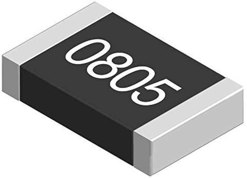
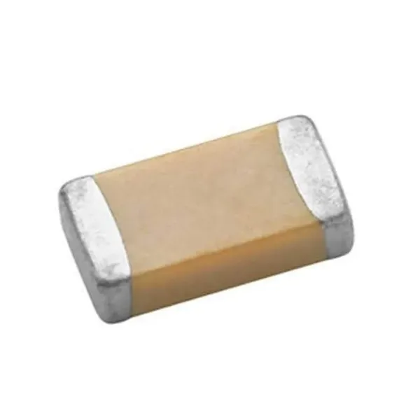
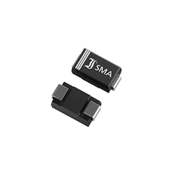
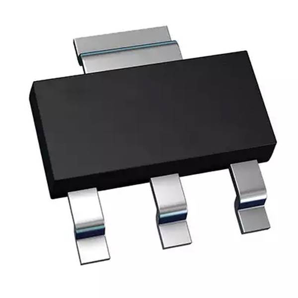
About electronic components
 |
 |
 |
 |
 |
| Resistor |
Capacitor |
Diode |
Mosfet |
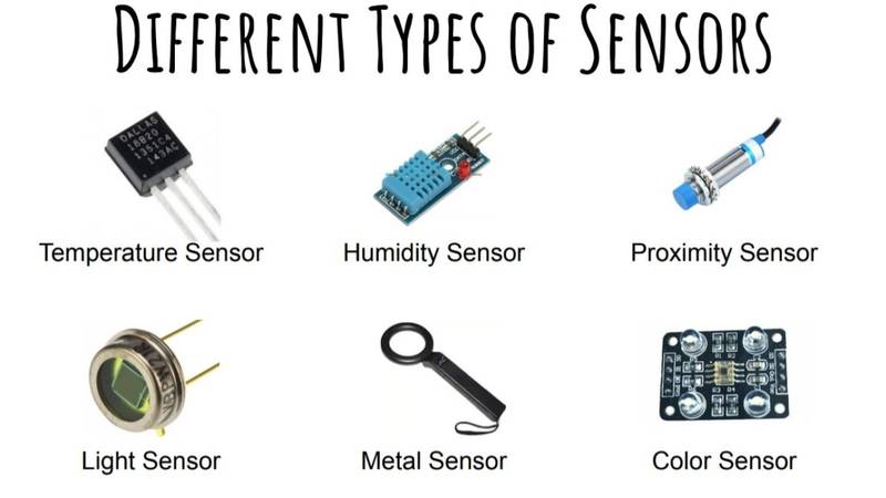
Sensor |
 |
 |
 |
 |
 |
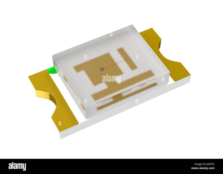
| LED |
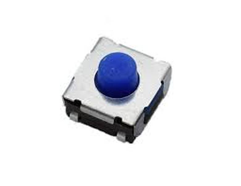
Tactile Switch |
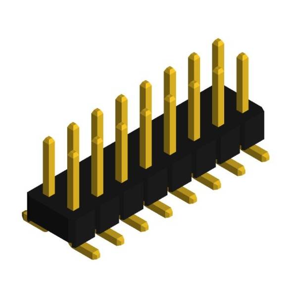
Pin Header |
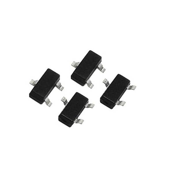
Transistor |
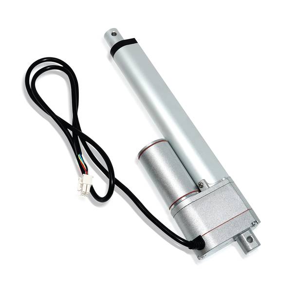
Actuator |
Type of Electronic Components
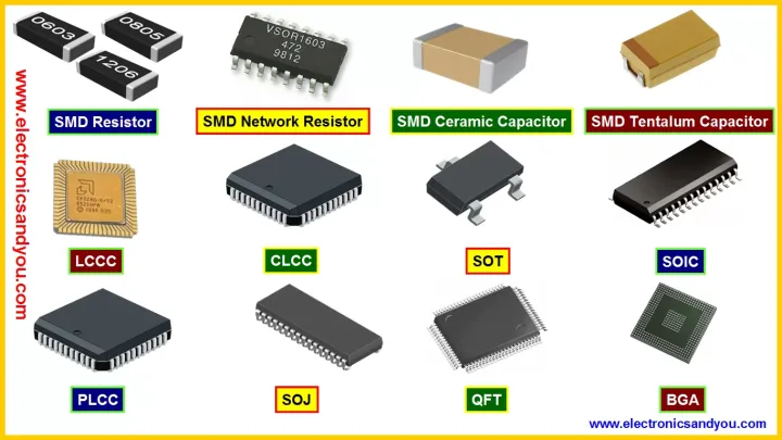
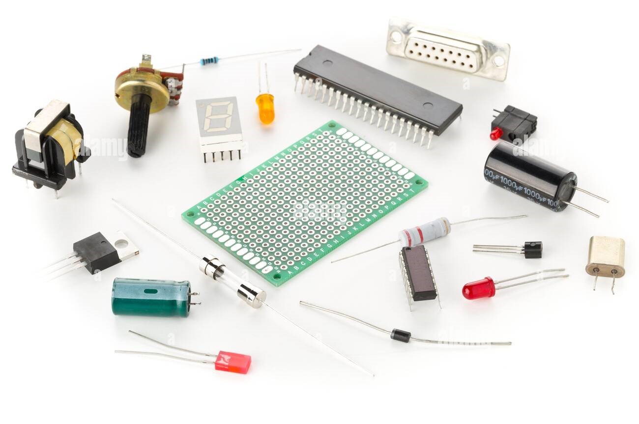
Components are of two types: SMD (Surface Mount Device) and Through-hole.
 |
 |
| SMD (Surface Mount Device) Components |
Through-hole Components |
Type of Electronic Components
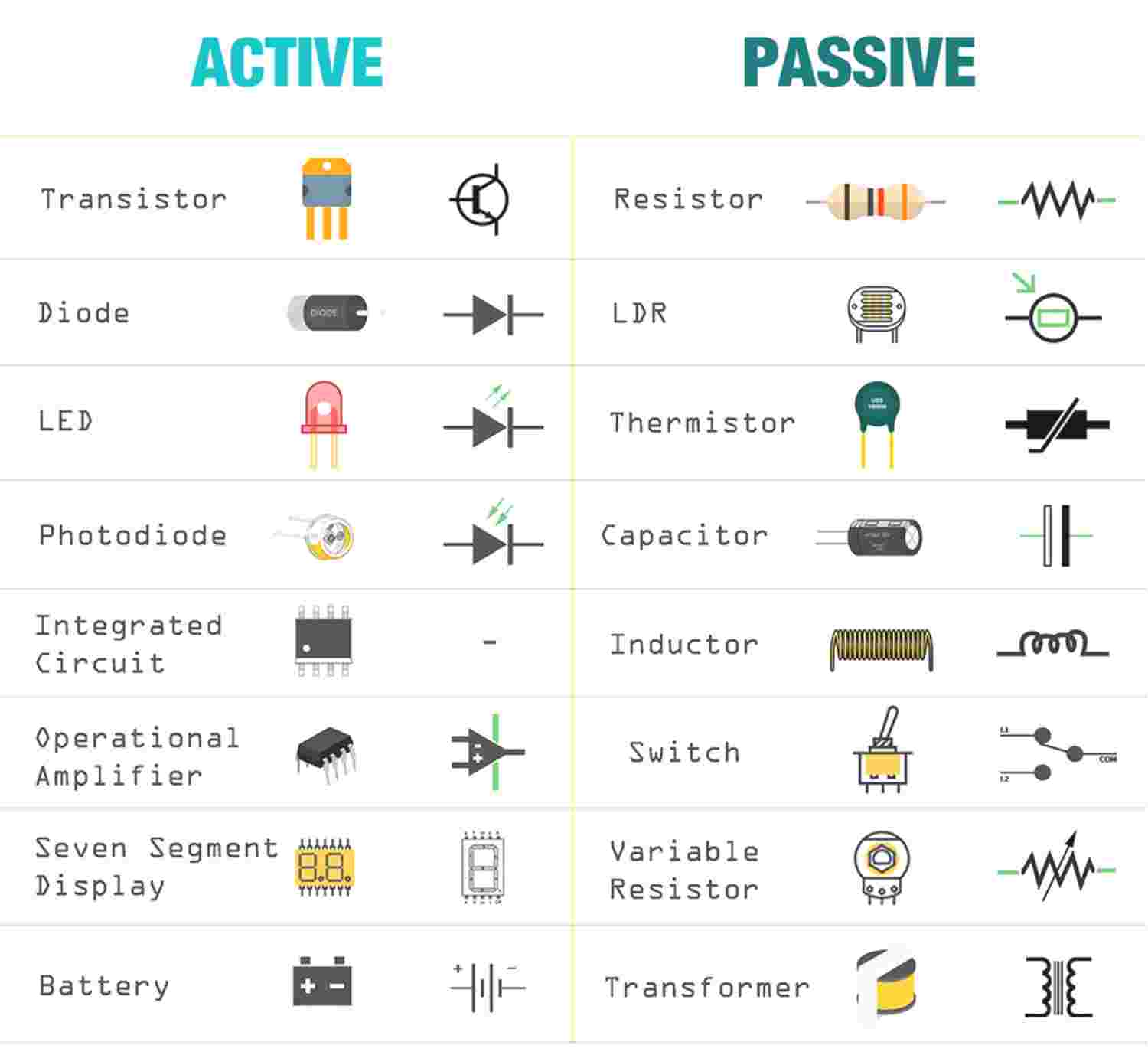
Components are of two types: Active and Passive components.
 |
|
| An example of active and passive components |
Individual Assignment
PCB Design tools
About DRC (Design Rule Check) and ERC (Electrical Rule Check)
I have used KiCad because --
KiCad has become a very popular choice for PCB design - Being open-source means a vibrant community contributes to its development, leading to continuous improvements and new features.
KiCAD Download Process
Please go through this link and follow the steps mentioned below: -
 |
 |
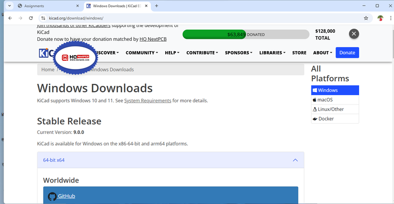
| First, click on the link above or visit the website "kicad.org" Then, click on the 'Download' option. |
After that, a new download page will open. Now, you can select the software based on your device and click on it. |
 |
 |
| After that, the software version page will open, and now you can click on 'Git' to download. |
Now, the software download will begin. Once the download is complete, you can proceed to install the software. |
Fab Library download
Please go through this link and follow the steps mentioned below: -
 |
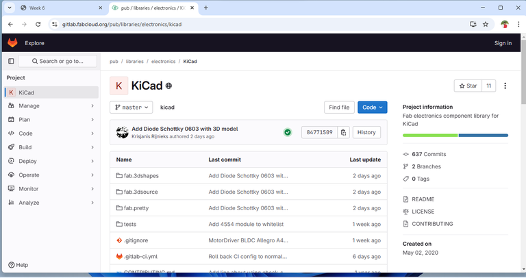 |
| First, click on the link above or visit the website "fab labraries" Then, click on the 'fabcloud.org' portal. |
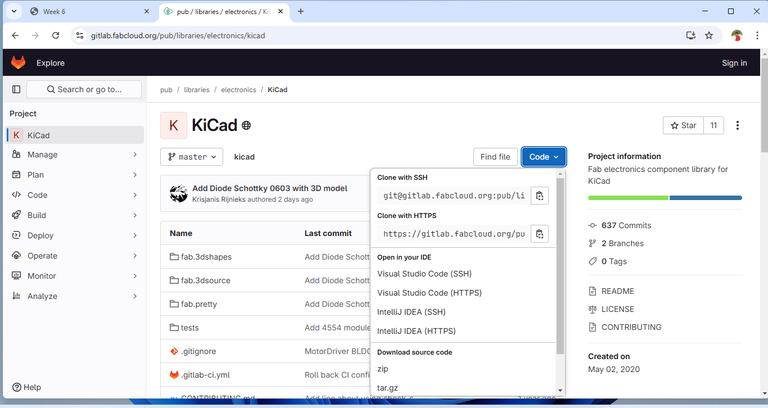
After that, the Fab Cloud page will open. Now, click on the 'Code' option. |
 |
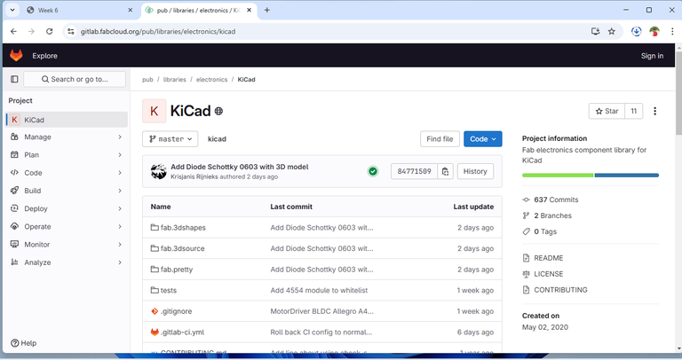 |
| After clicking on the 'Code' option, click on 'Download ZIP' to begin the download. |
Now, the fab libraries will begin to download. |
Fab Library setup in kiCAD
 |
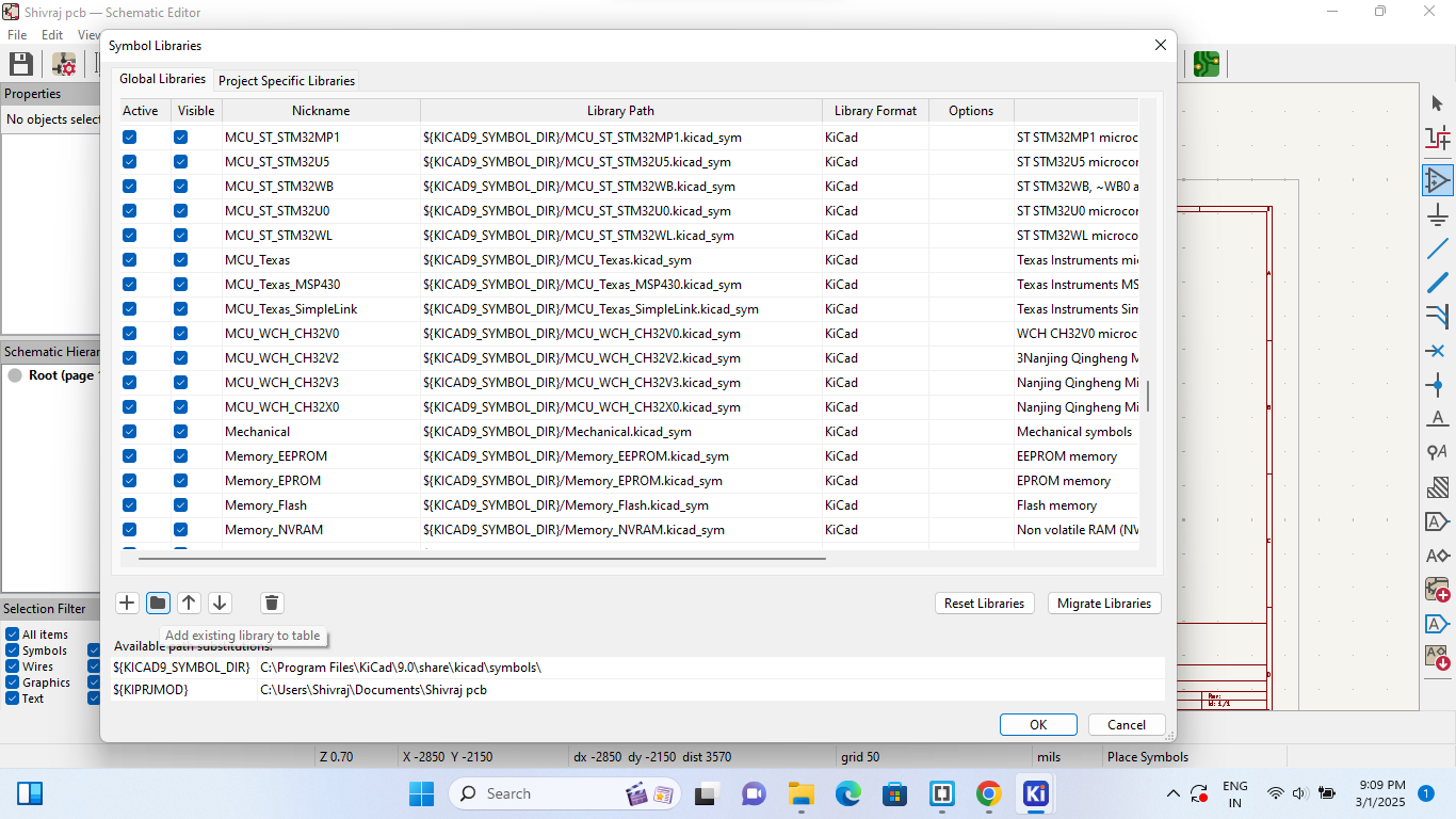 |
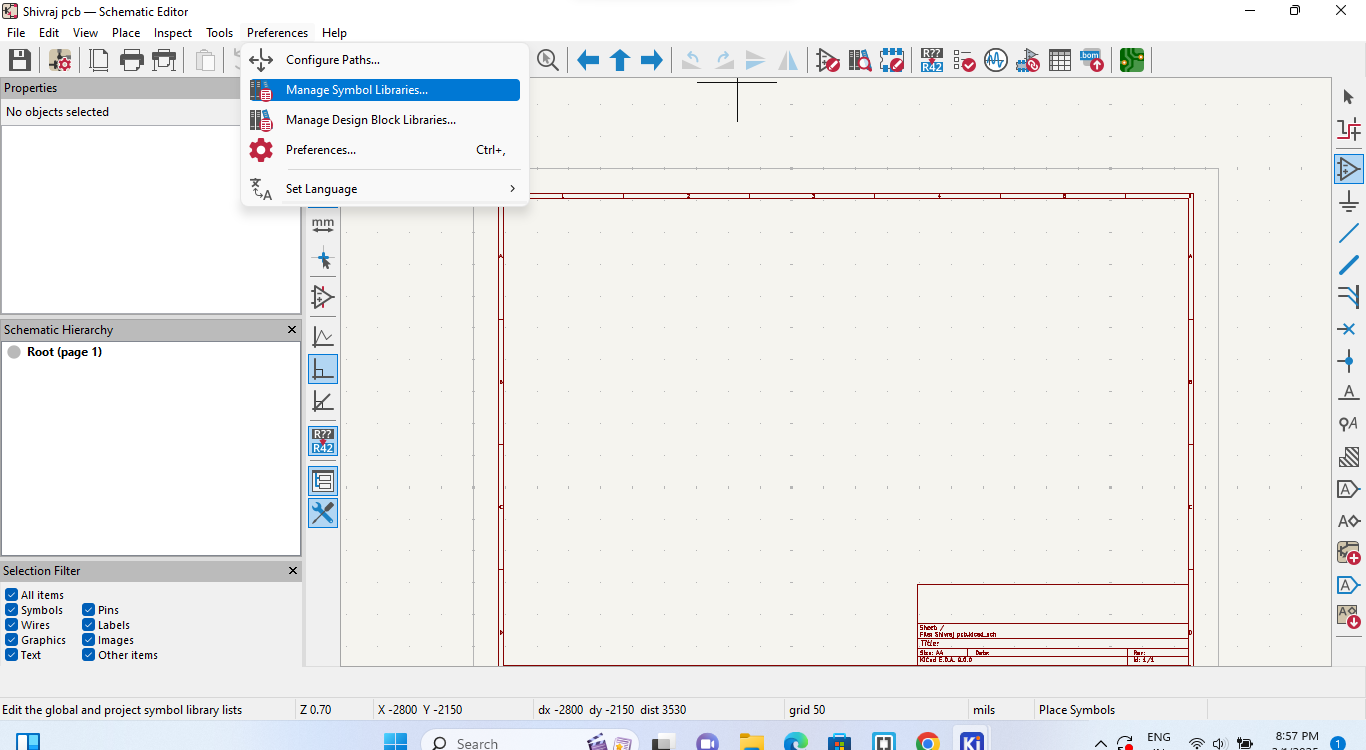
| First, Open the preference and select the "Manage Symbol Libraries" |
Then Select folder option |
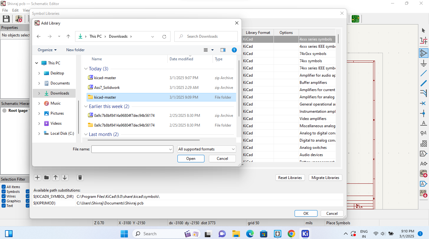 |
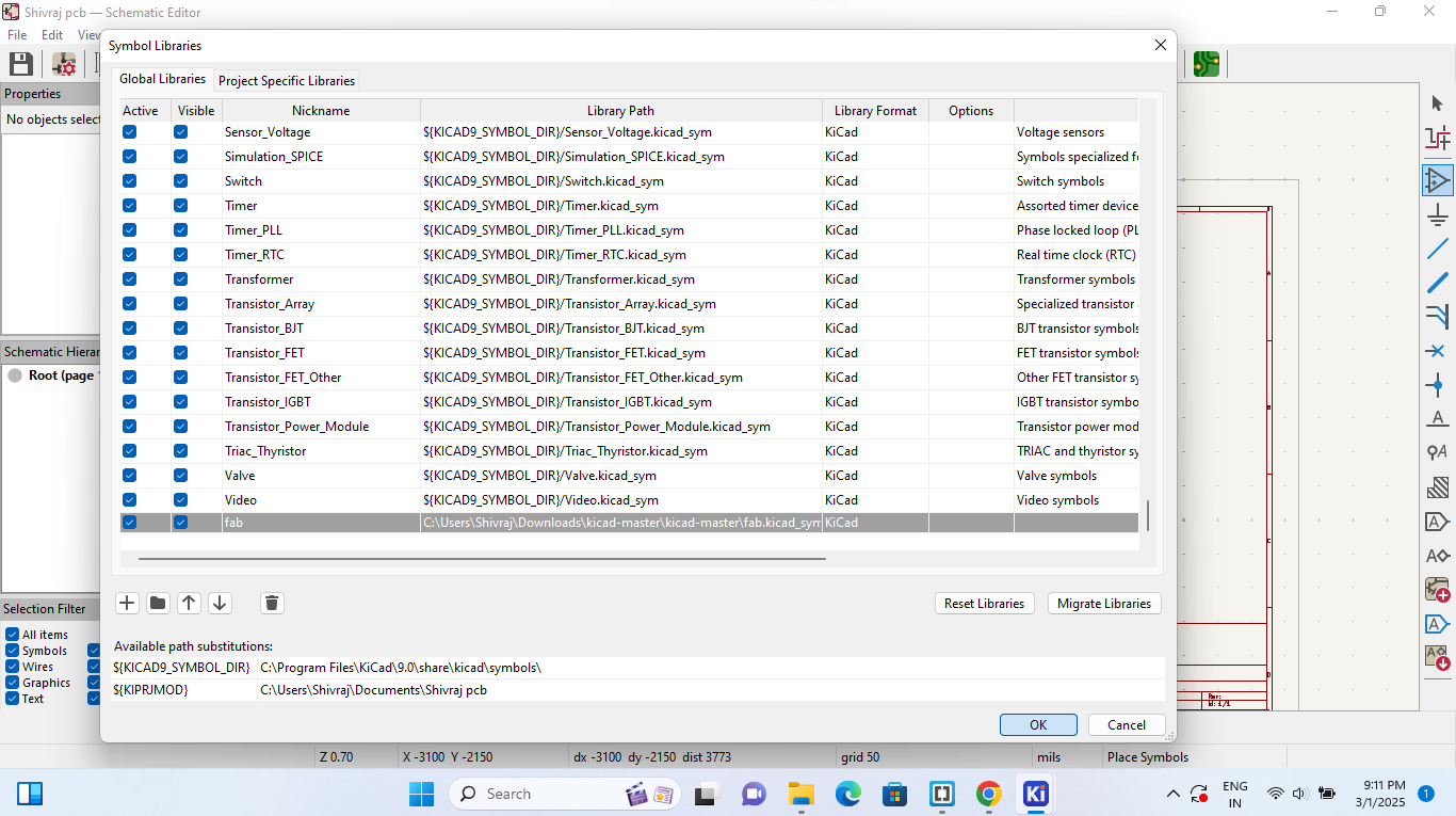 |
| Click on the folder option and select fab library file from the device |
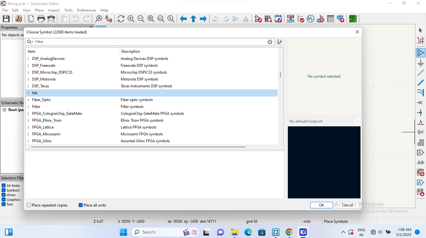
Now the feb library will visible in KiCad library |
 |
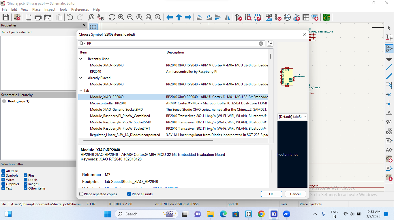 |
| Now, We can search this feb librry and components in KiCad |
|
PCB Schematic Designing
KiCad is a powerful open-source tool for designing PCBs, from schematics to manufacturing files.
 |
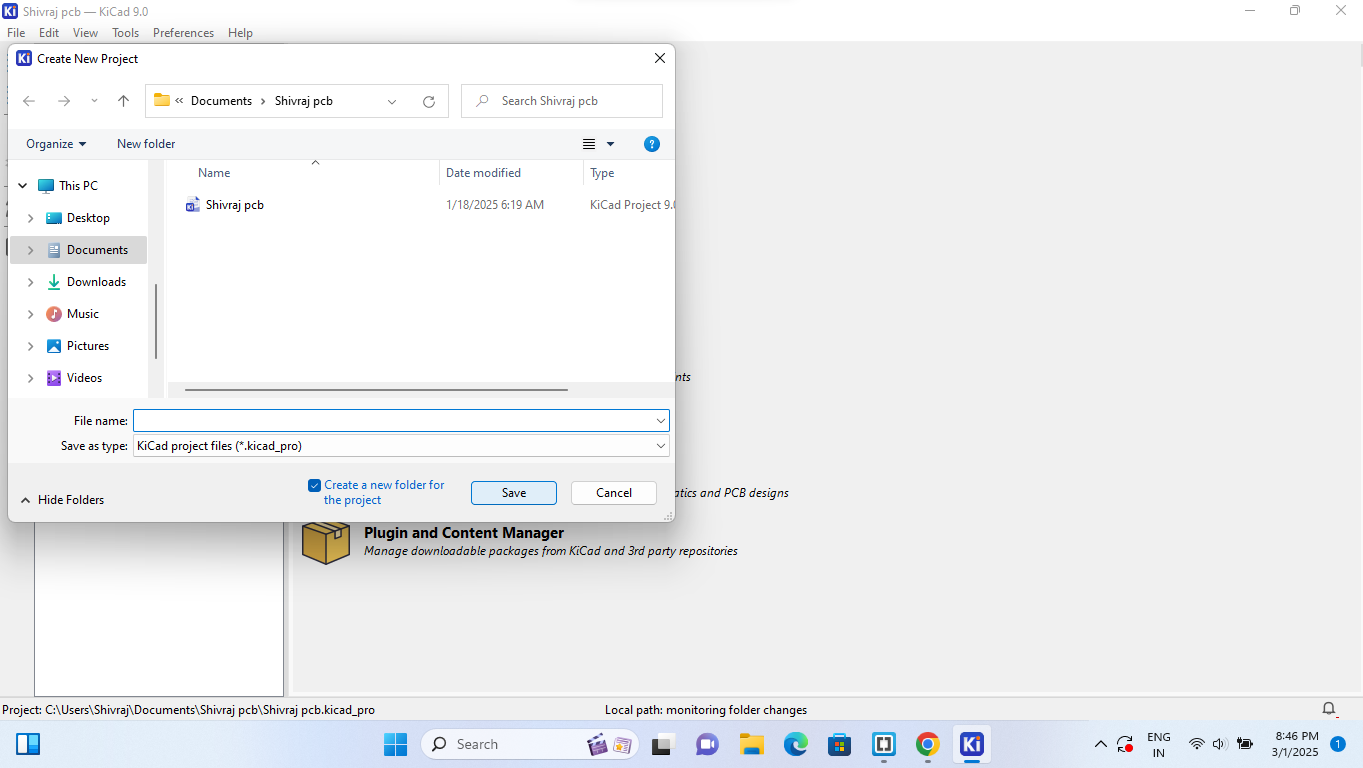 |
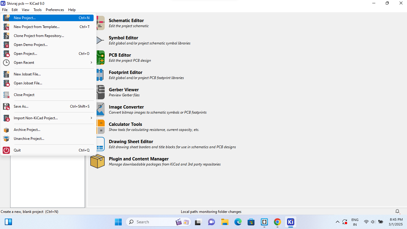
| First, open KiCad. Then, click on the "File" menu and select "New File" |
Save new file to device |
 |
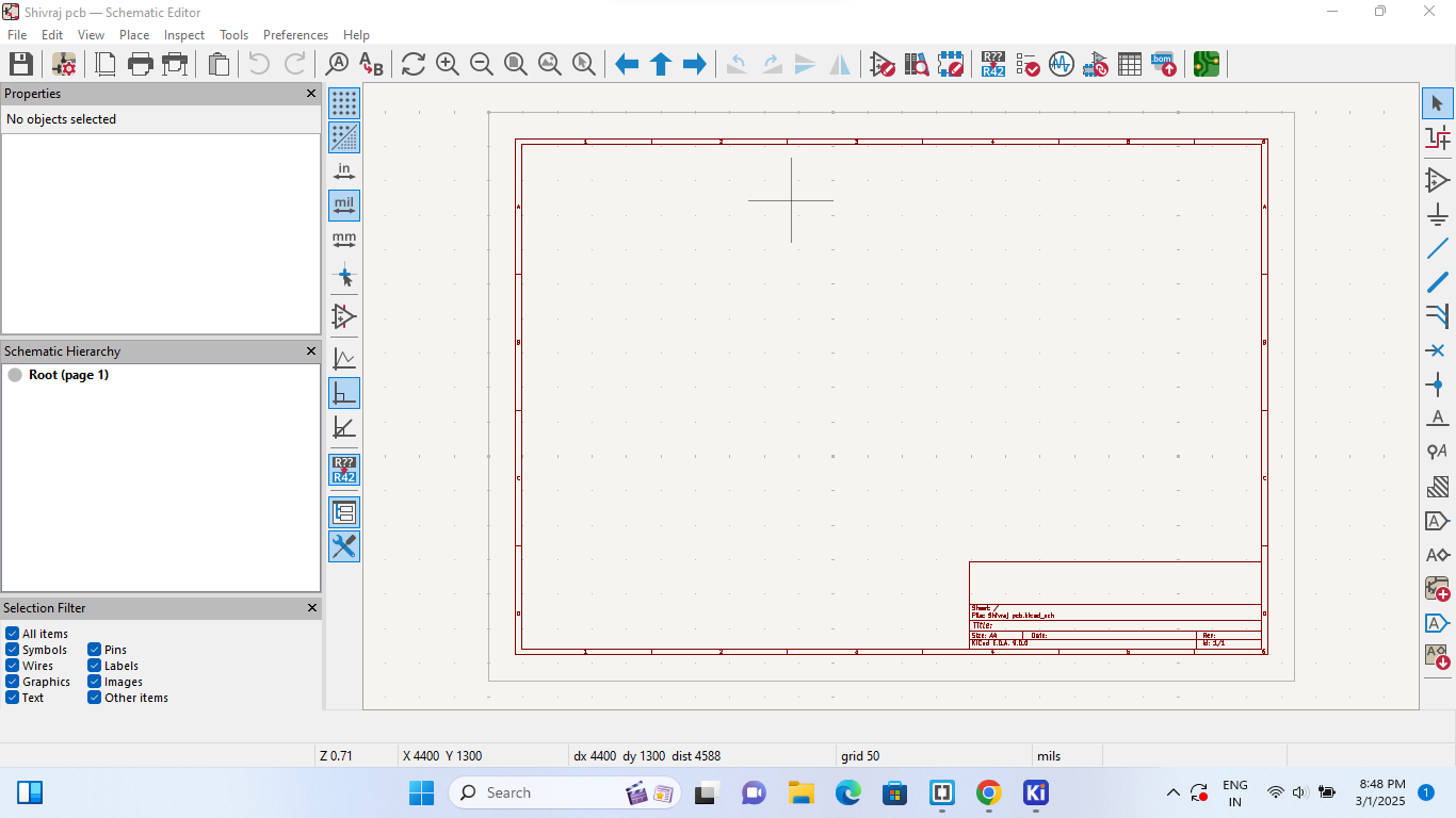 |
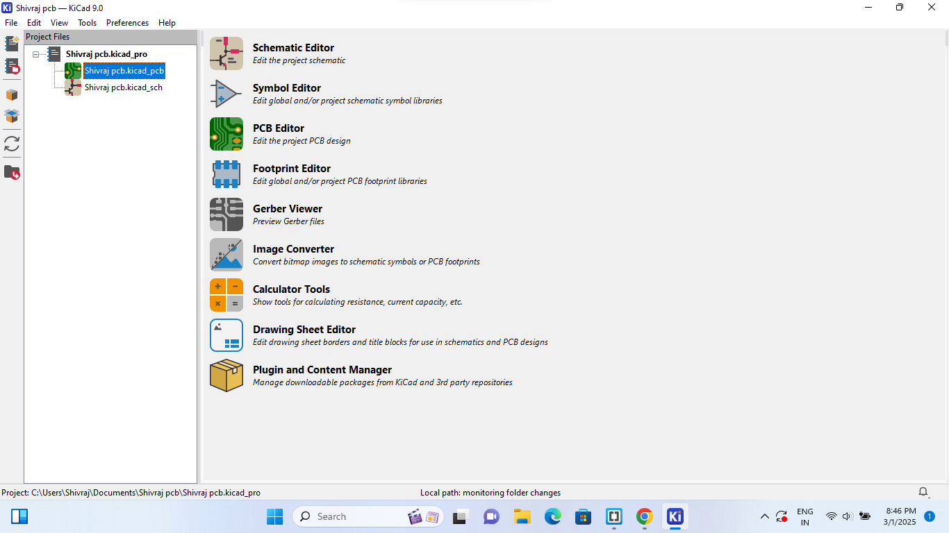
| After this, KiCad will generate two files: one for the "Schematic" and the other for the "PCB Layout". Then, select the "Schematic File". |
After this, the Schematic Editor workspace will open. |
 |
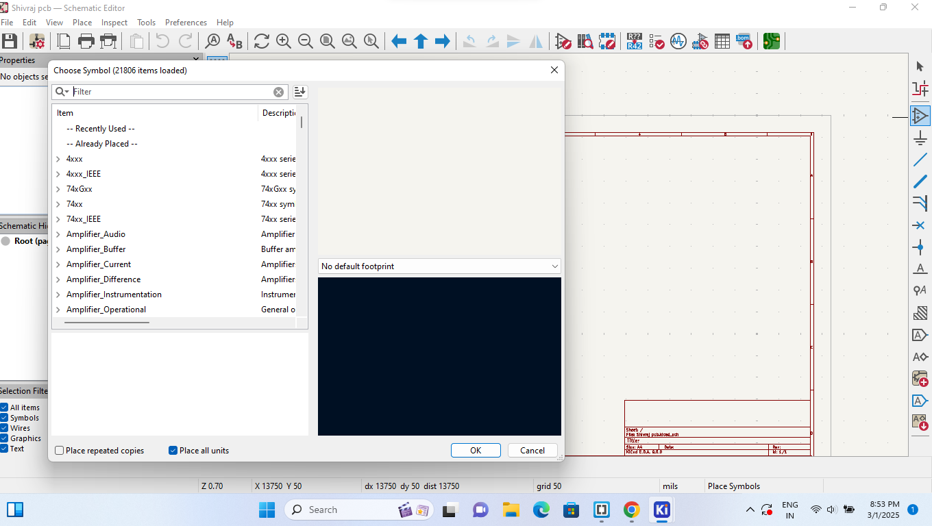 |
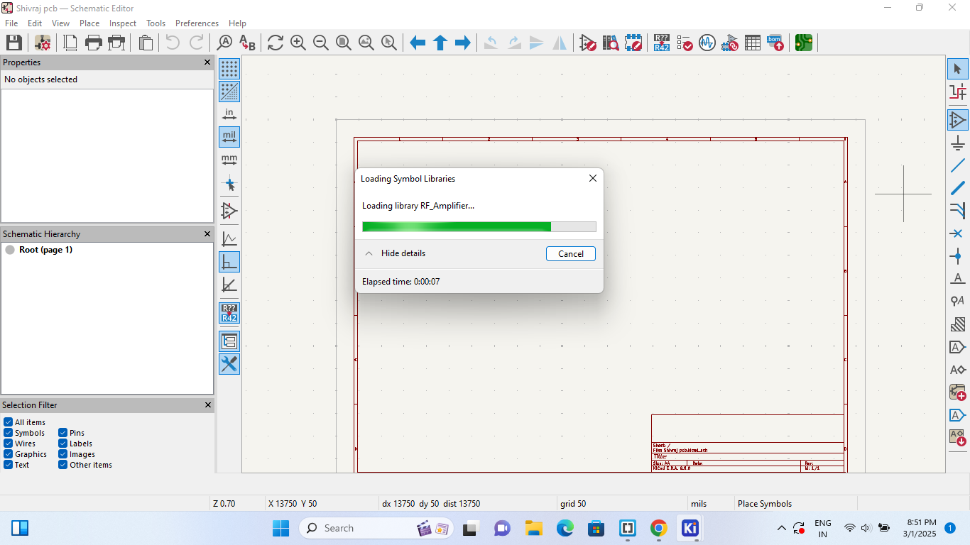
| After this, clicking on "Place Symbol (A)" will open the library |
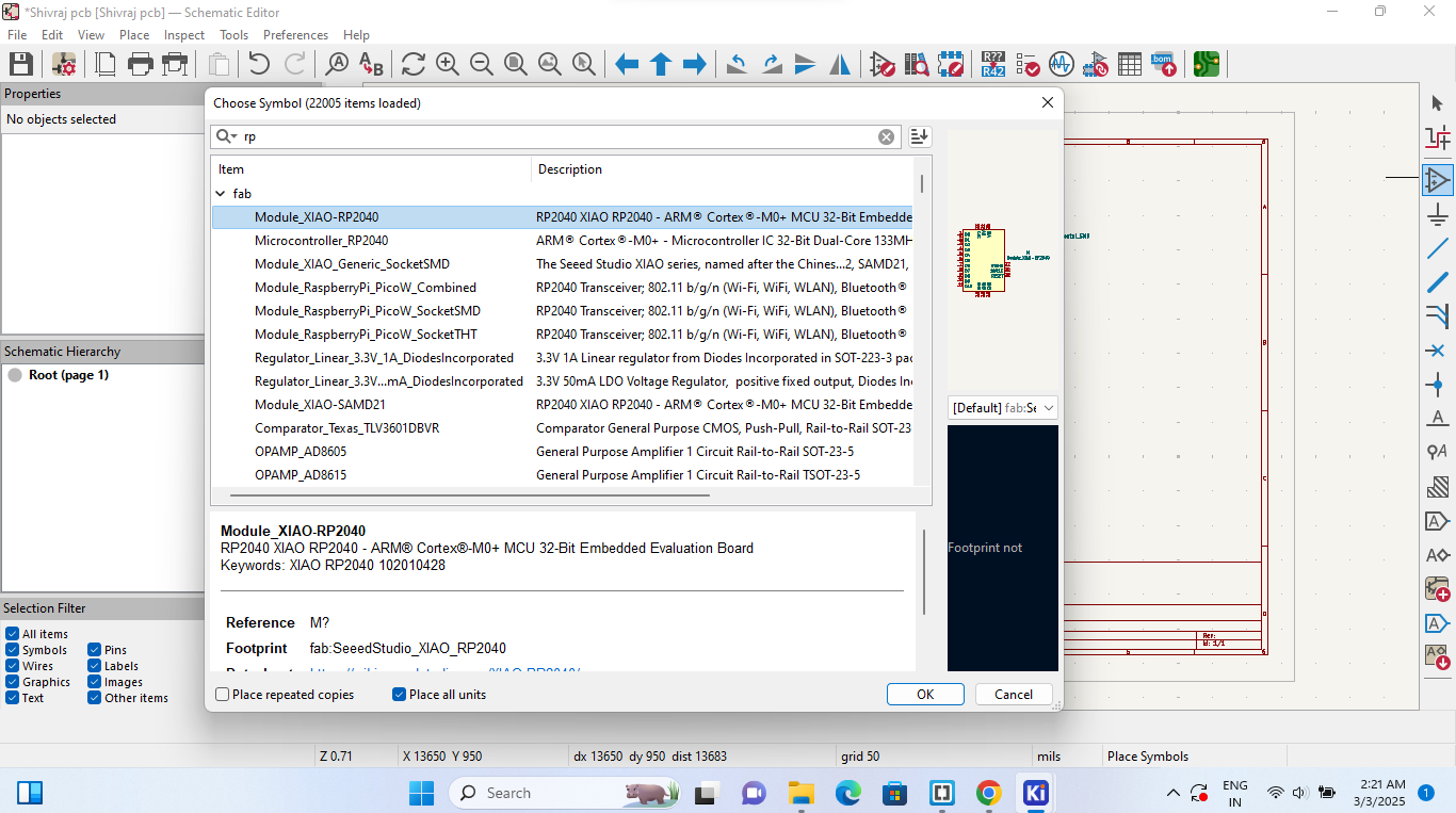
Now, you can view the available components in the library. |
 |
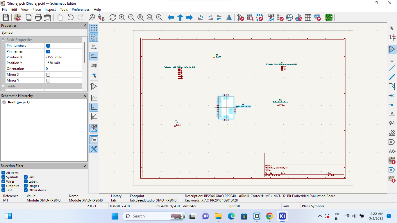 |
| Select the components based on your PCB requirements. |
After selecting the components, place them in the workspace. |
 |
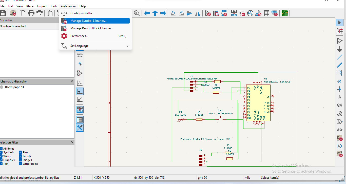 |
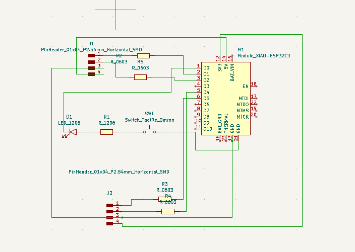
| I selected the "Xiao ESP32C3 module" and added the required components. Then, connect all the components using the "Draw Wire" option. |
After completing all the wire connections, I opened the "Preferences" menu and selected "Manage Symbol Libraries" to assign footprints. Then, I added the footprint file. |
PCB Layout Design
After finalizing the schematic, the next step is placing components and routing traces on a PCB
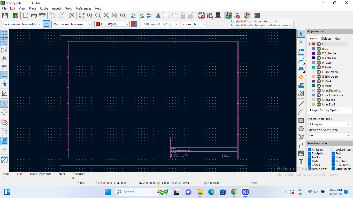 |
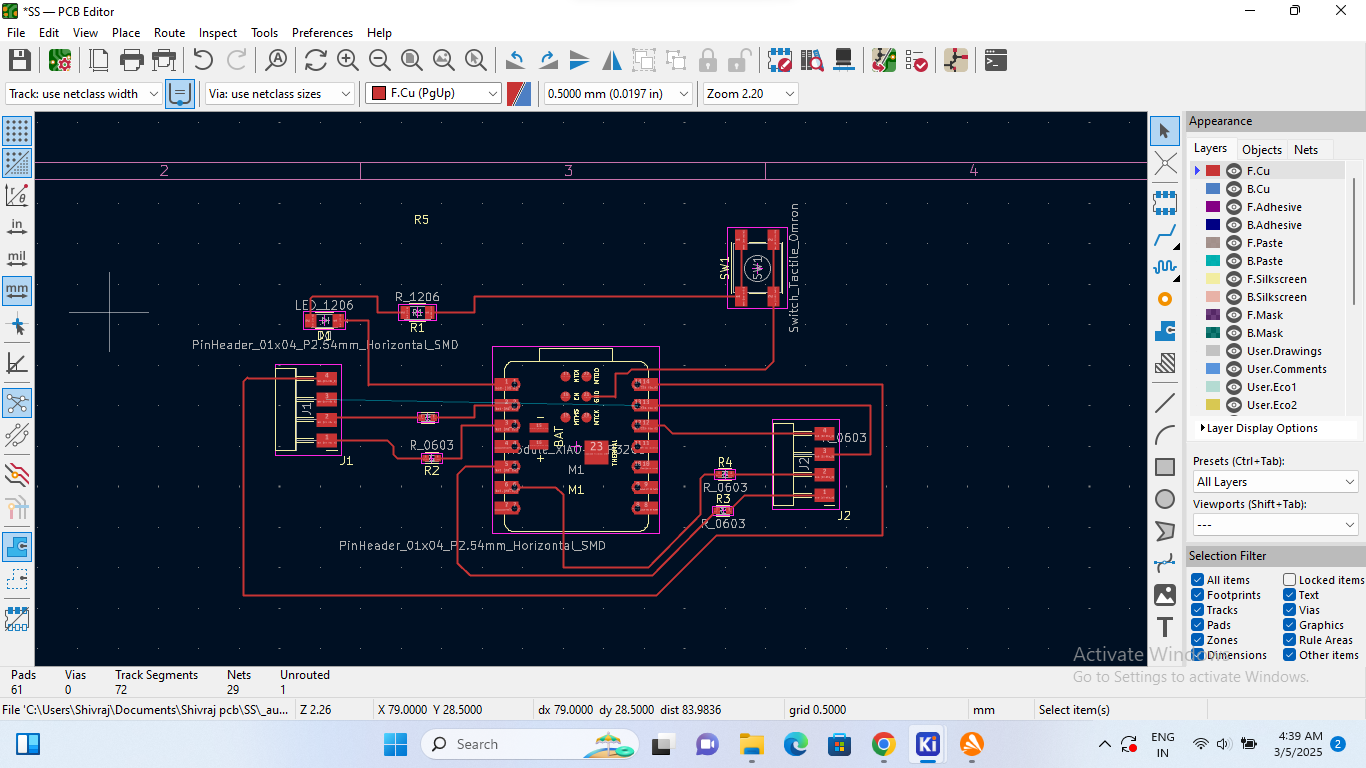 |
| After this, I clicked on "Switch to PCB Editor" and then selected "Update PCB from Schematic" to apply the changes and routing the components. |
Then, I carefully placed all the components in the correct positions and drew the copper traces and connected all components. |
 |
|
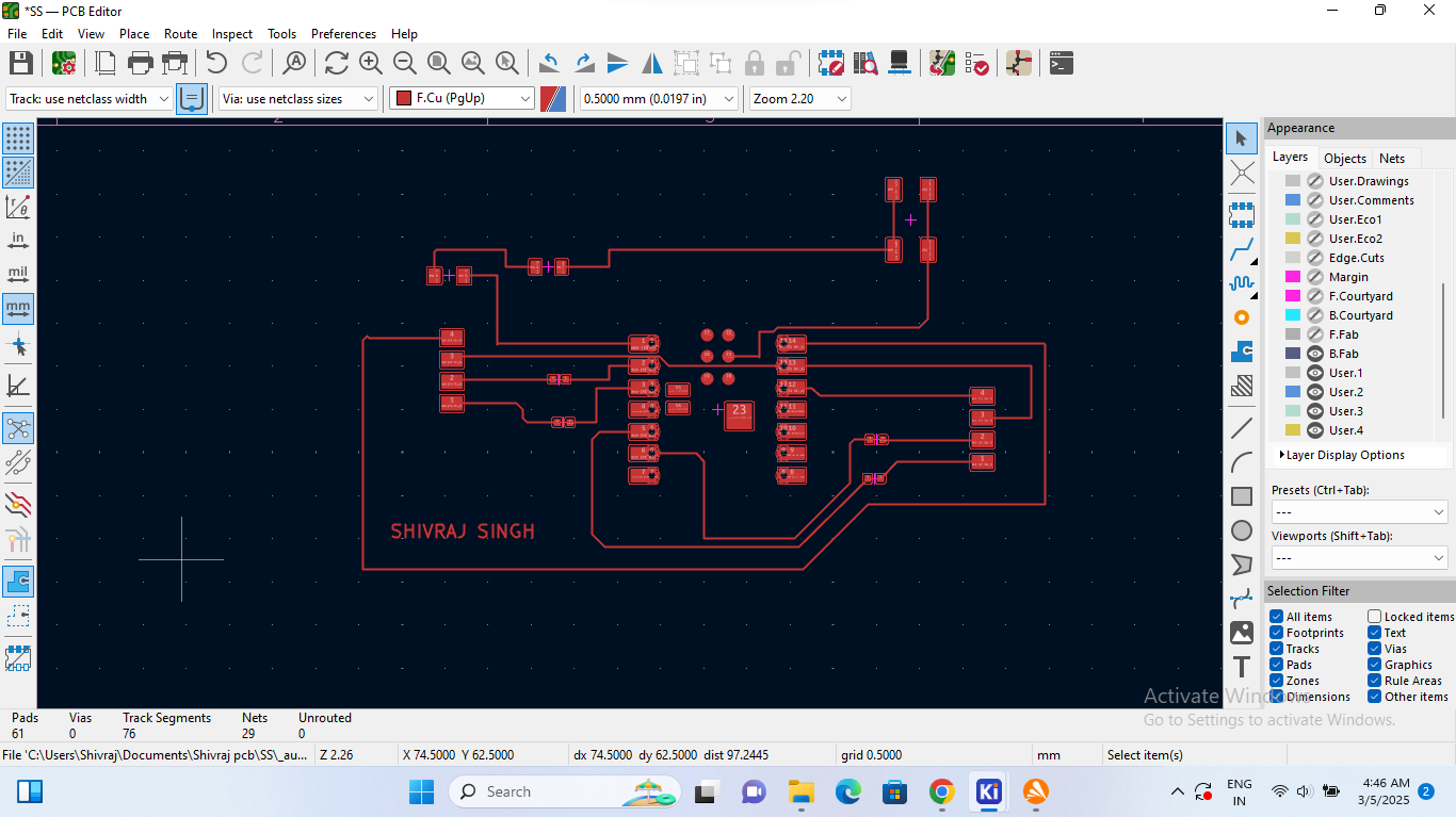
| After that, I removed all the "Airwires" (Ratsnest Lines) and finalized the copper traces. |
|
Parameters of PCB track
As I have already explained the PCB design process above, I realized that I had not mentioned the width of the copper tracks and the clearance between two tracks. Therefore, I would like to specify here.
Edge Cut (PCB Outline) and 3D Viewer
 |
|
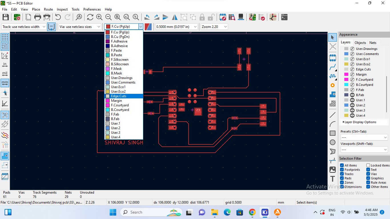
| Now, I selected the "Edge Cut" option. |
|
 |
 |
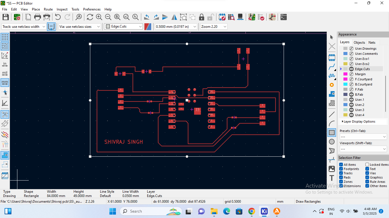
| After that, I draw a rectangle around the PCB design using the Edge Cut layer to define the PCB boundary & outer line. |
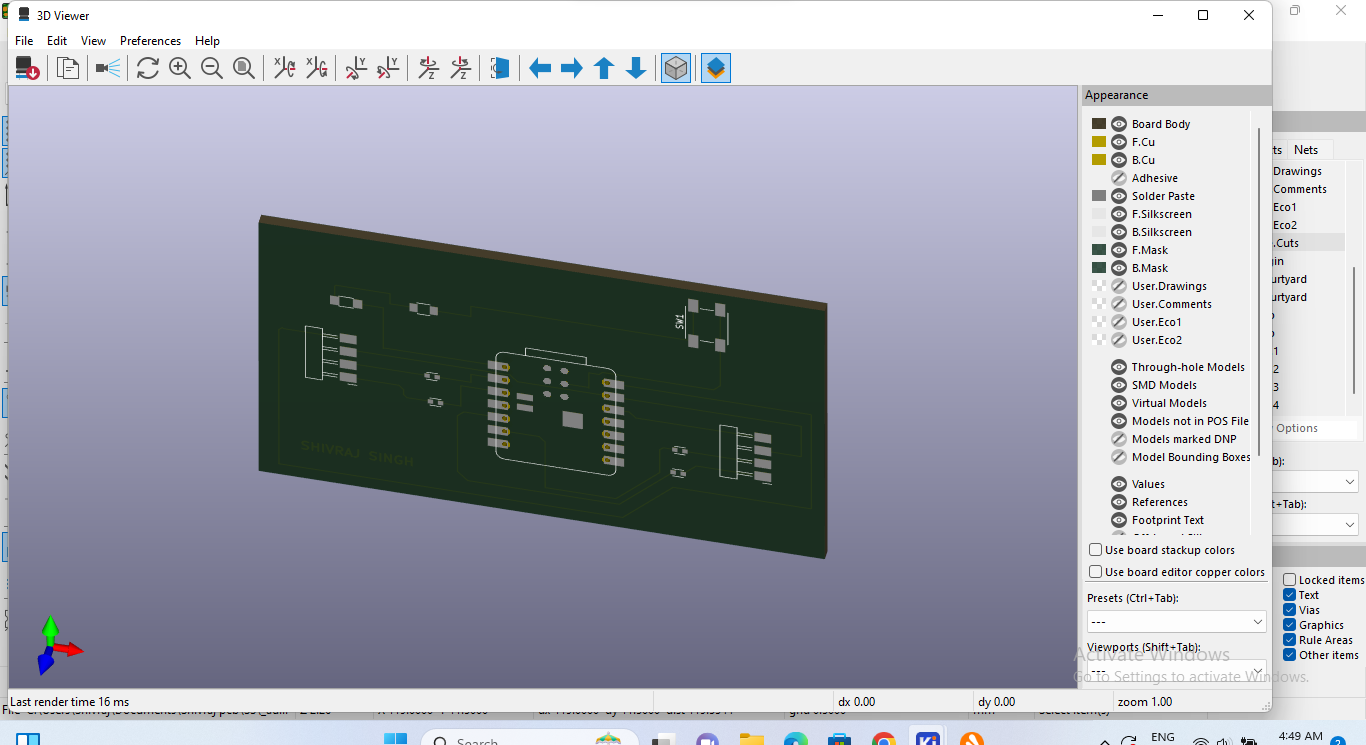
Then, I clicked on the "3D Viewer" option to visualize the PCB design in a 3D view. |
Gerber File Generation (For PCB Fabrication)
 |
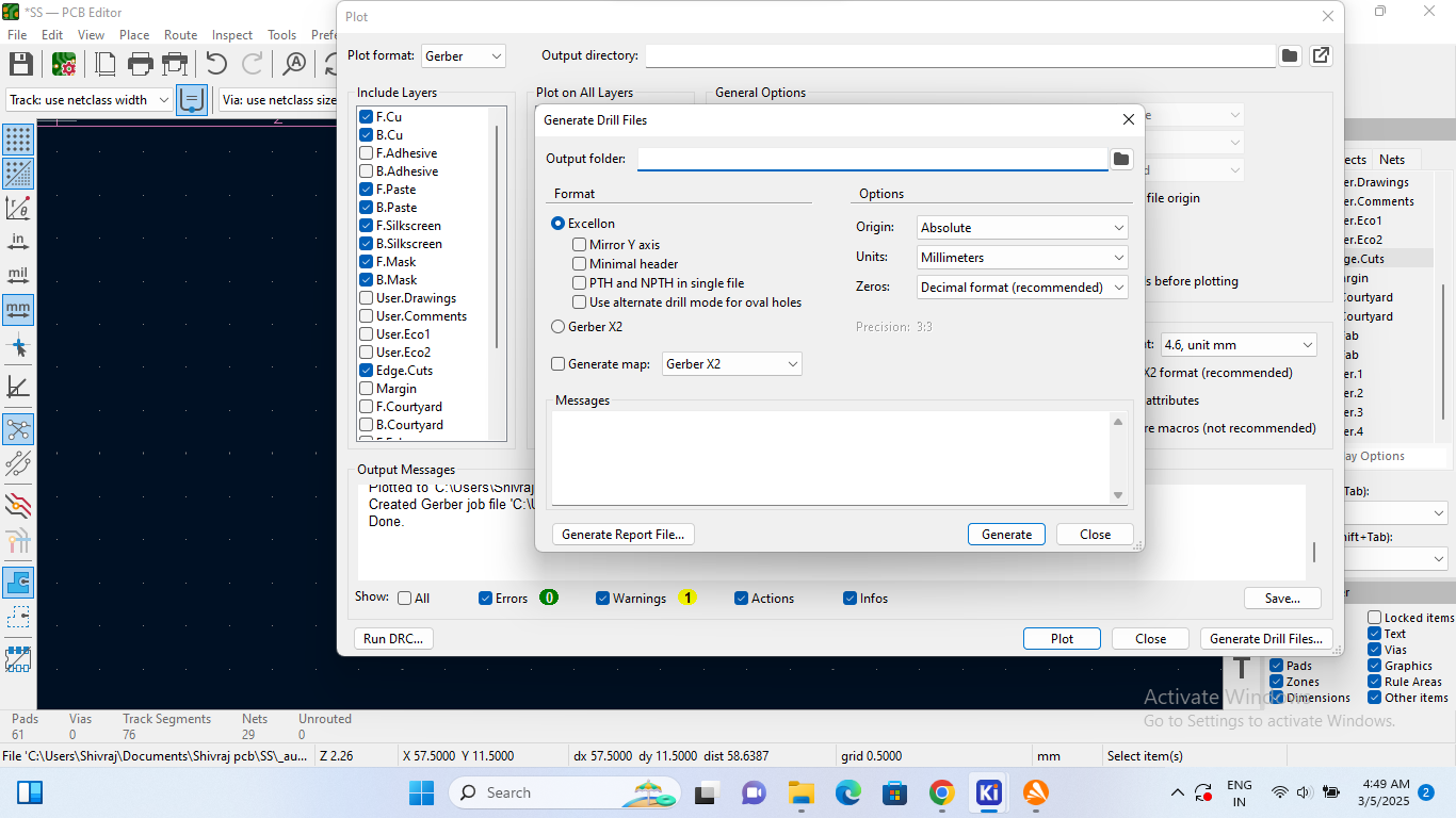 |
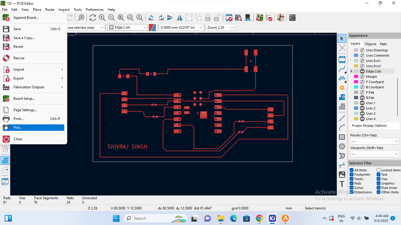
| Now, to save the design, I went to the "File" menu and clicked on the "Plot" option. |
Next, in the "File Format" option, I selected +Gerber File" and generated the final file |
 |
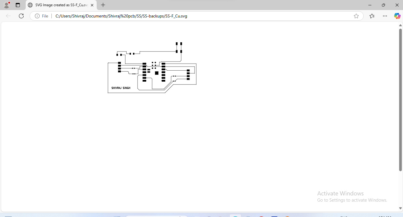 |
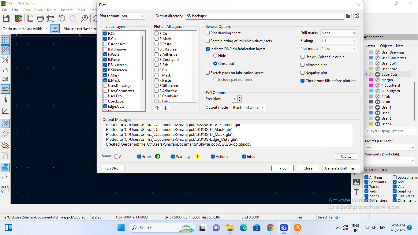
| After that, I followed the same process to save the file in "SVG" format. |
PCB Layout in SVG Format |
Download Original File's
Download edge cut file in SVG formet here
Download in cut file in SVG formet formet here