
System Integration
About This Week
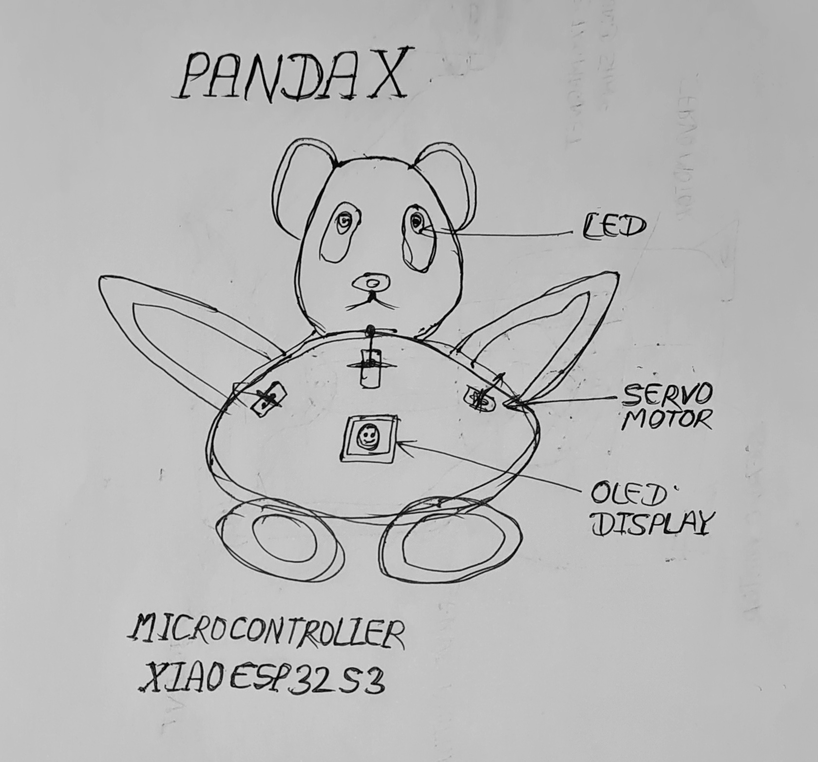
This week's main objective was to plan and understand how the final project will work, including identifying the necessary components and how they will be connected and function together. The focus was on thorough preparation and planning for the final implementation, ensuring that I have the correct components, a well-defined circuit layout, and a solid foundation to proceed with building and testing the final prototype.
Heroshot of the Assignment
 |
 |
|
|
|
Objctive of the Assignment
1. Individual Assignment
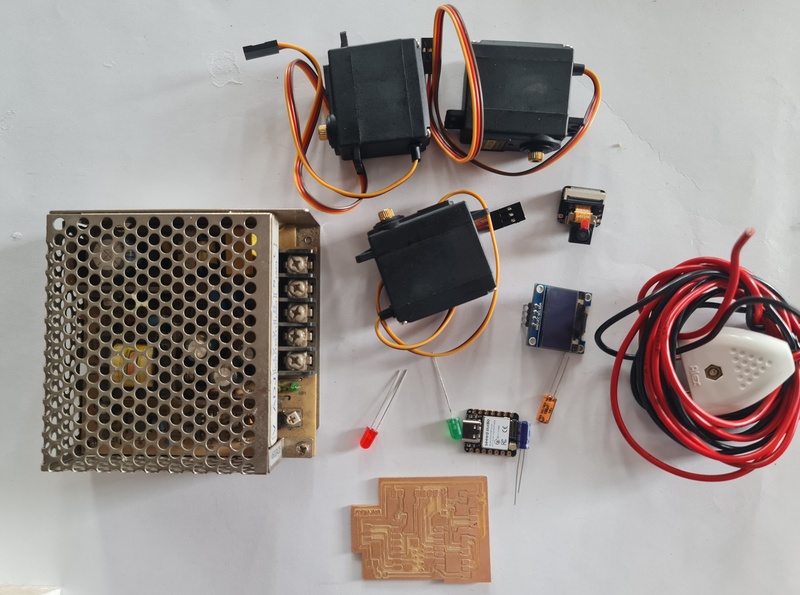
Hardware Components will Use in the Project
|
|
List of the Components
| Component | Quantity |
|---|---|
| LEDs | 2 |
| XIAO ESP32 C3 Sense (CAM Module) | 1 |
| MG99 Servo Motor | 3 |
| OLED (I2C) | 1 |
| 4 Pin Connector | 1 |
| 3 Pin Connector | 4 |
| 2 Pin Connector | 3 |
| Capacitor 100pf | 1 |
| Capacitor 4.7uf | 1 |
| Resistance SMD 0E | 1 |
| Resistance SMD 499.1k | 1 |
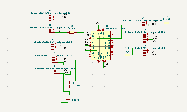
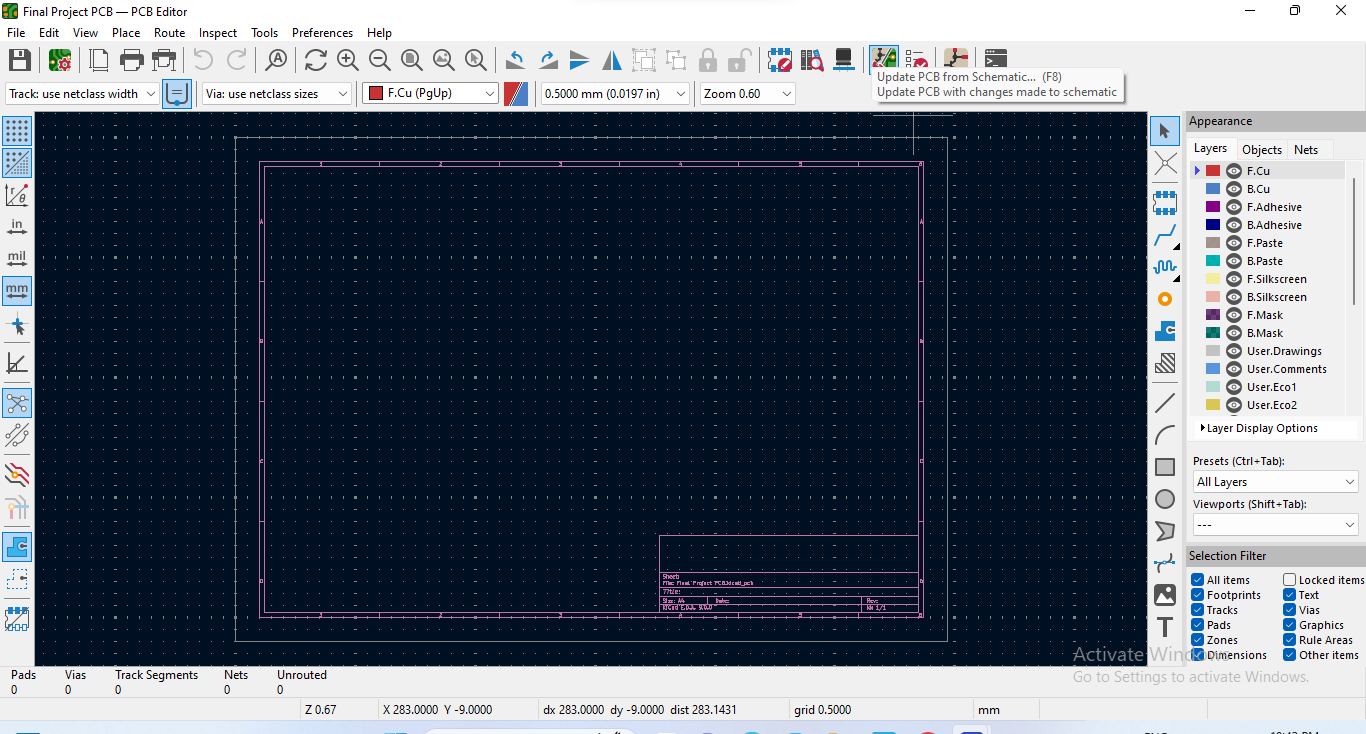
PCB Design
|
| PCB Designing and Placement of Components in Schematic section. |
|
| Proceeding to the PCB Editor Section. |
|
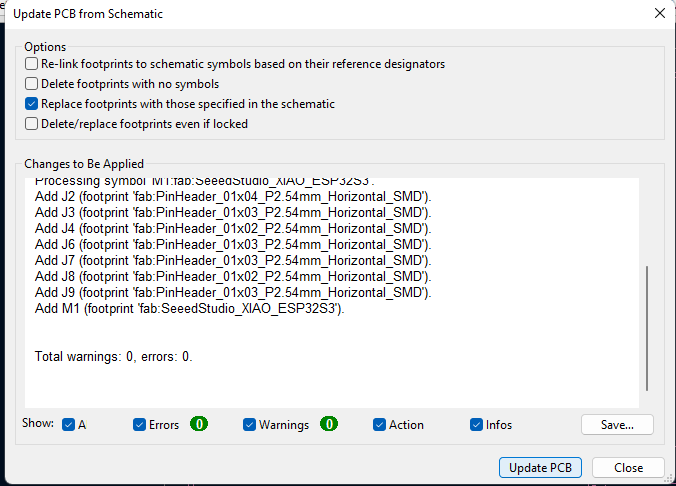
| Updateing PCB from the Schematic Section. |
|
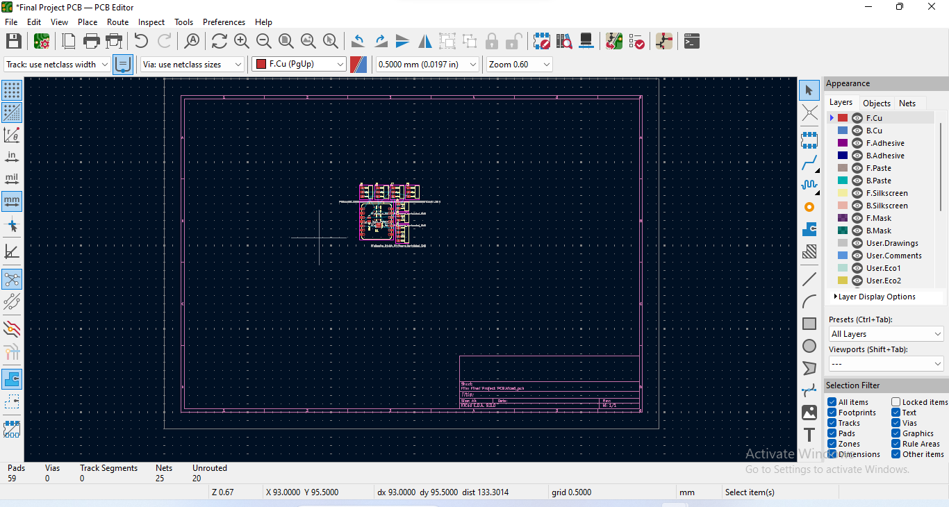
| Updated PCB |
|
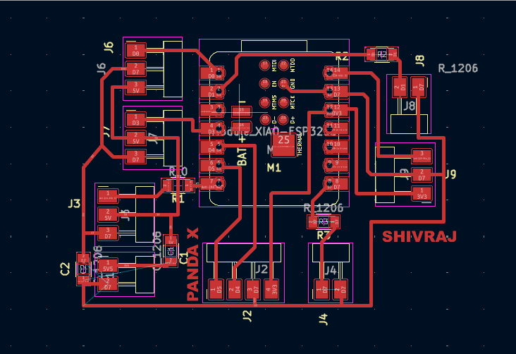
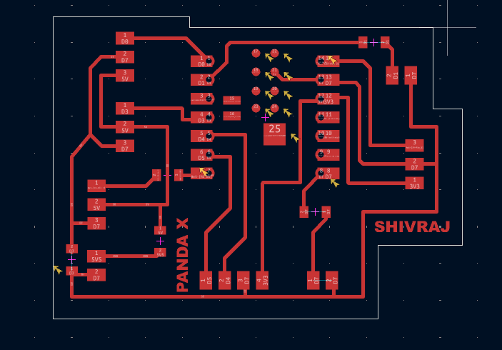
| In this step, all the electronic components were carefully placed in their appropriate positions on the PCB, following a logical and organized layout. Proper placement is crucial to ensure efficient routing, minimize interference, and maintain a compact design. |
|
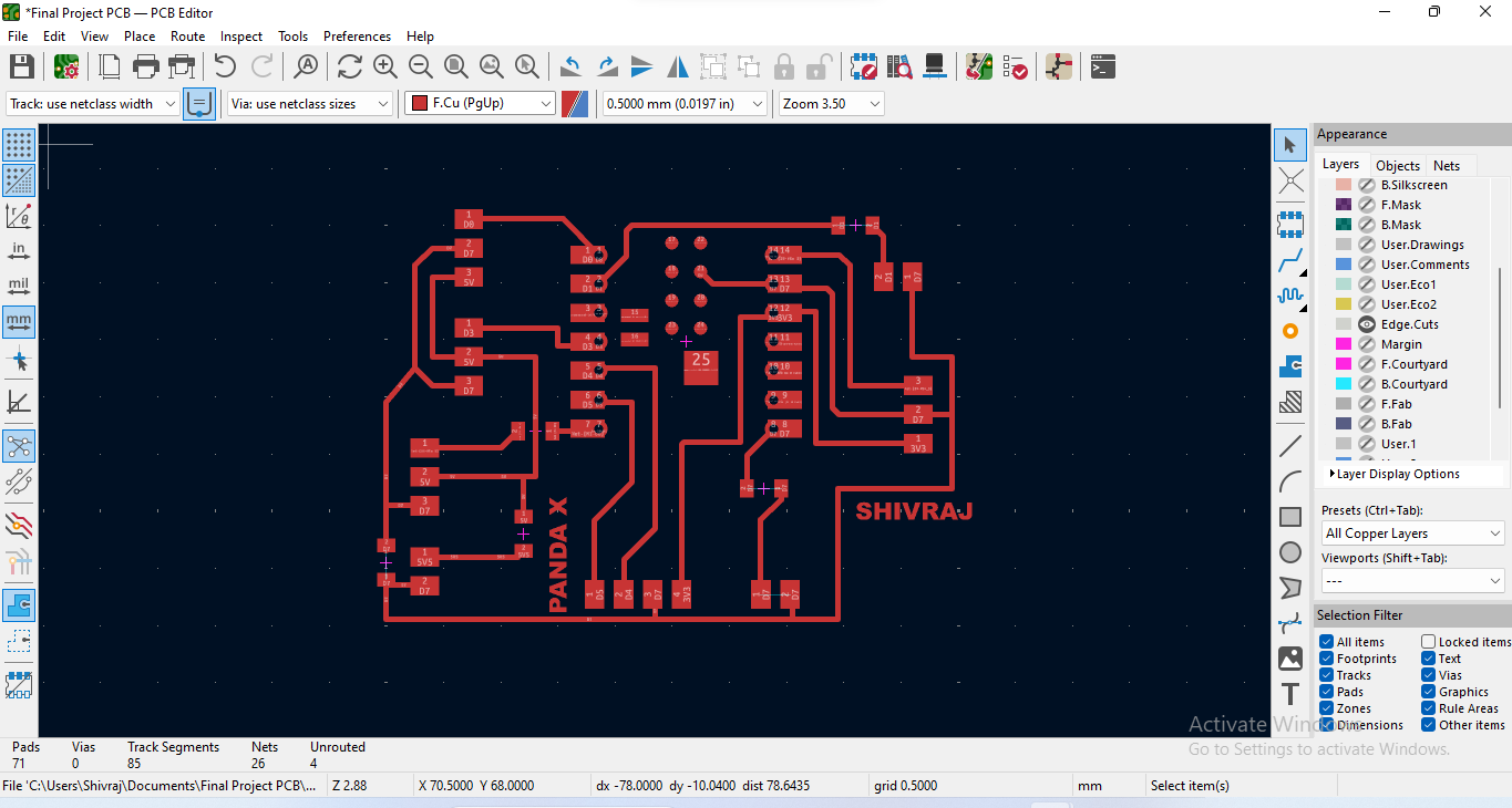
| All unnecessary parts were hidden, and only the copper layer was kept visible to ensure the PCB is displayed clearly and prints properly. |
|
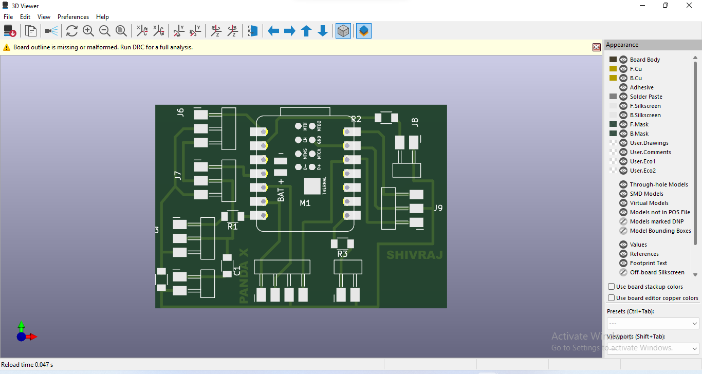
| After that, the PCB was viewed in 3D mode to visualize the final design and check the placement of all components accurately. |
|
| Then, the edge cut was made to define the exact dimensions and shape of the PCB for final fabrication. |
|
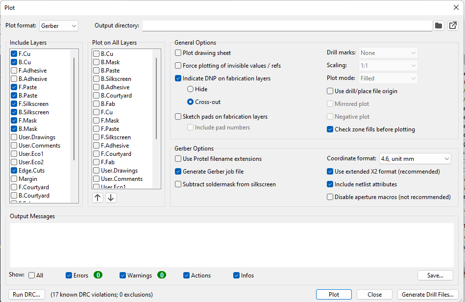
| Finally, the PCB design was exported as a Gerber file, which is the standard format required for PCB manufacturing. |
PCB Milling ( SRM 20)
For PCB milling, I first downloaded the design in Gerber format and then converted it to PNG format using an online tool (link provided below). After that, I used Mods CE to generate the toolpath from the PNG file and downloaded it. Finally, I used the VPanel software to operate the milling machine and started the PCB cutting process.
Gerber to PNG and SVG formet converter here
|
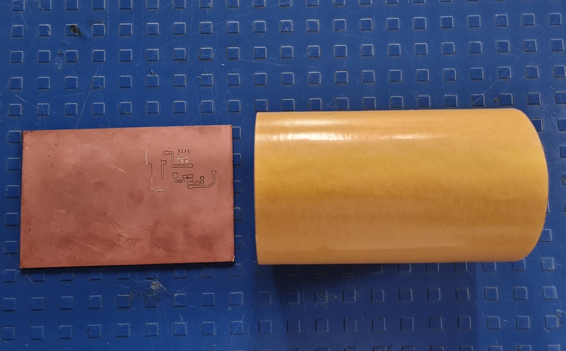
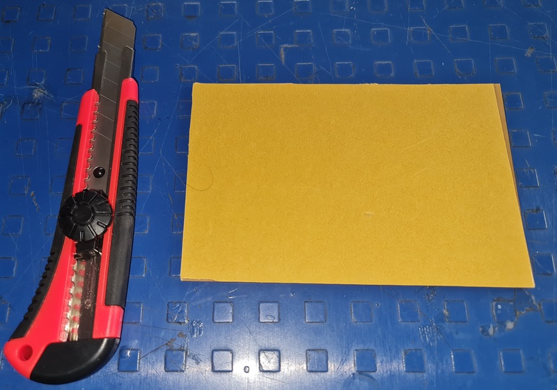
| Using FR4 PCB Material and Masking Tape |
|
| The masking tape was carefully applied to the back side of the PCB to hold it firmly in place during the milling process. Using a knife, the unnecessary or excess tape around the edges was neatly trimmed to ensure a clean and precise setup for cutting. |
|
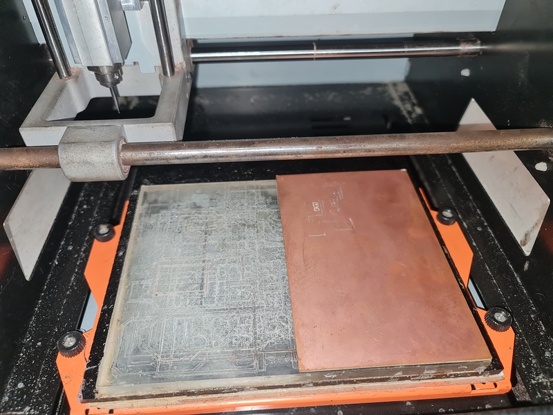
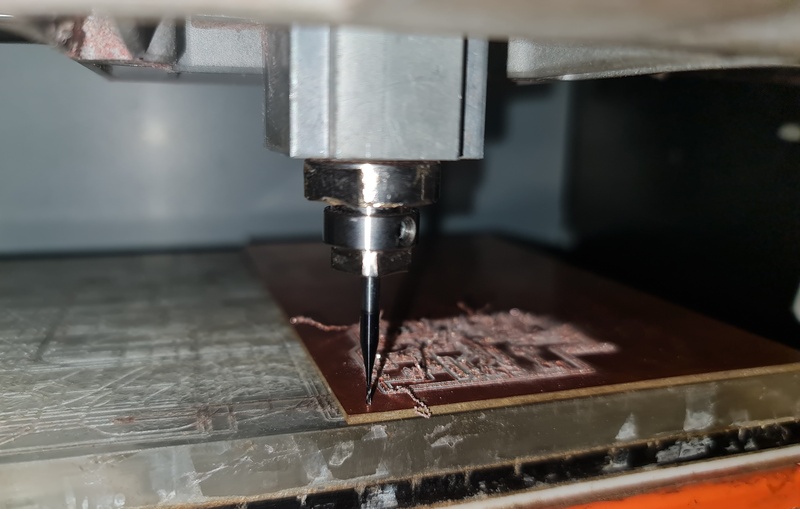
| The PCB properly fixed on the milling machine bed to ensure stability and accuracy during the cutting process. |
|
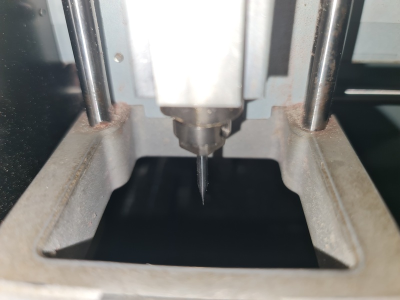
| 1/64-inch bit was putted for tracing the PCB. |
|
| Then, the bit was set on the bed to level it properly for accurate cutting. |
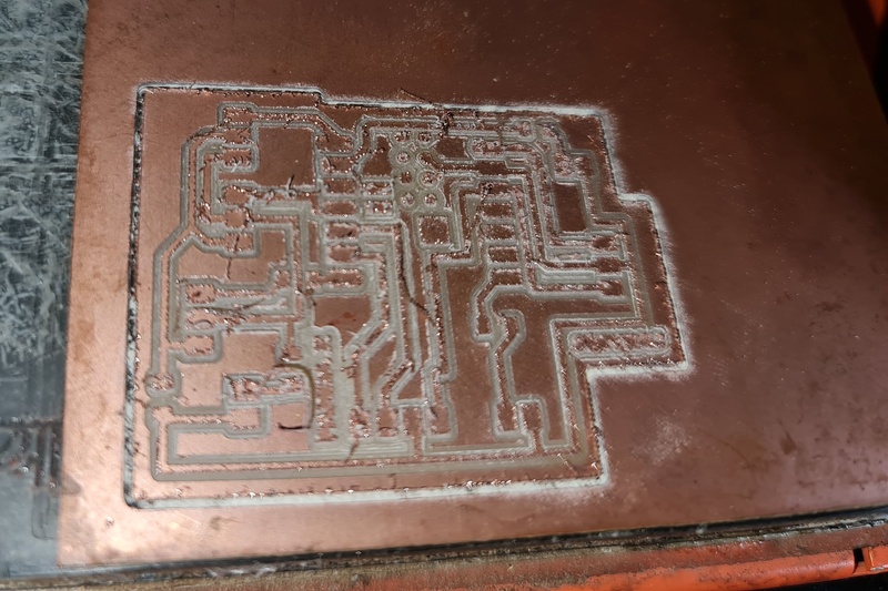
Started the machine for trace cut
|
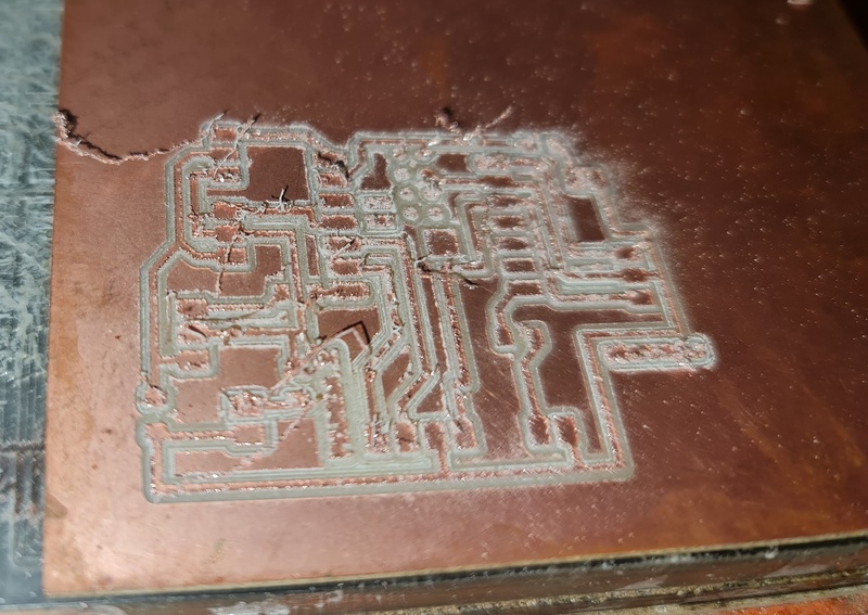
| Trace cut complated. |
|
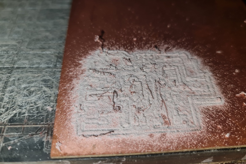
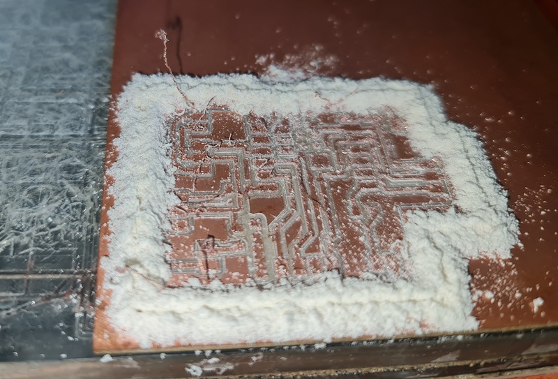
| Once the PCB trace was milled, the surface was cleaned using vacuum cleaner to remove dust and ensure the traces were clearly visible. |
|
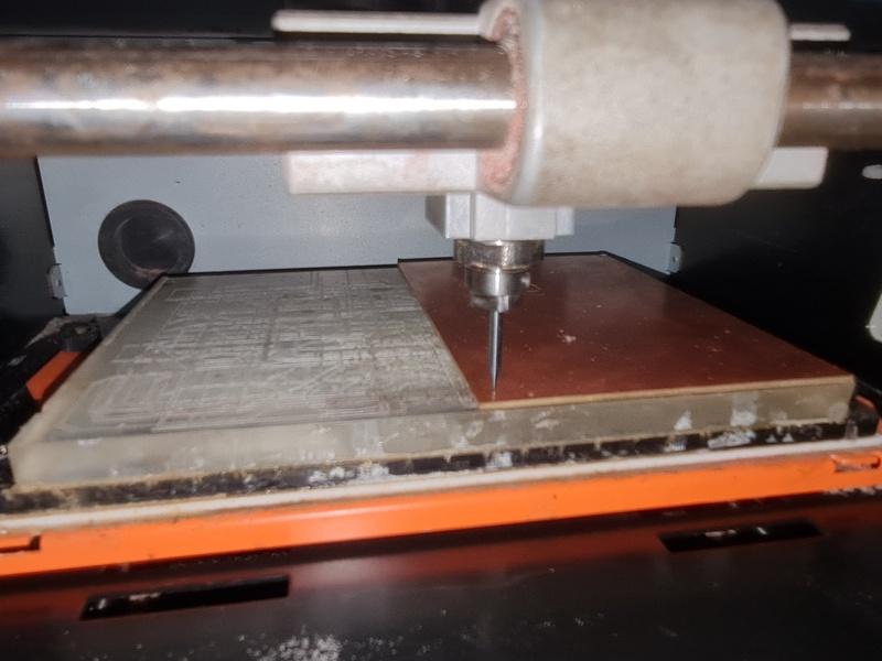
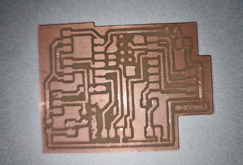
| After that, the bit was changed to a 1/32-inch bit for edge cutting, and gravity leveling was checked again on the machine bed. |
Started the machine for edge cut
|
| Edge cut completed. |
|
| Once the PCB edge cut was milled, the surface was cleaned using vacuum cleaner to remove dust and ensure the traces were clearly visible. |
|
| Finally, the PCB was removed from the machine and thoroughly cleaned using a brush. |
|
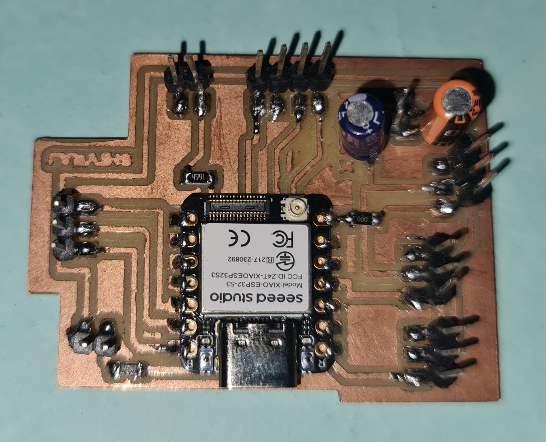
| The PCB was fully assembled with all components soldered in place. |
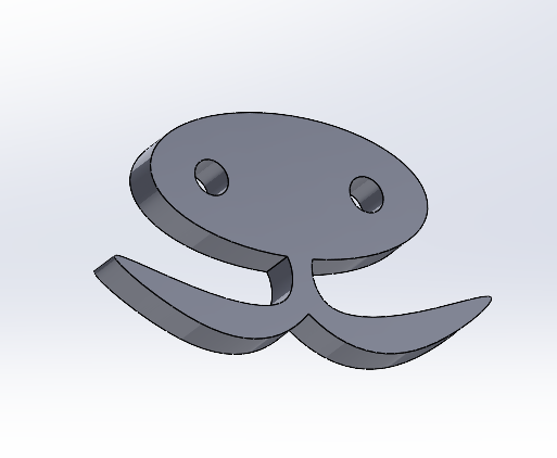
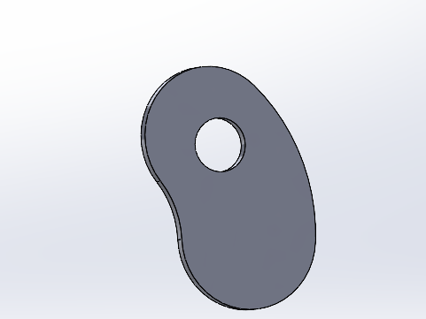
2D Designing Panda in solid work
 |
 |
 |
 |
|
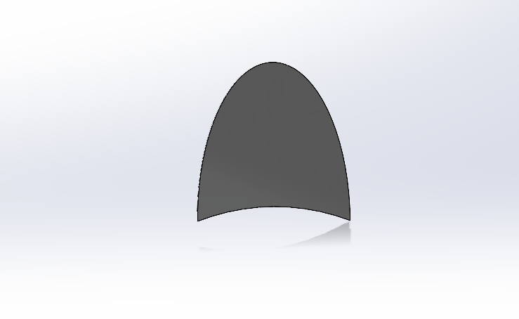
| Ear |
Foot |
Hand |
Head |
|
 |
 |
 |
 |
|
| Front Side Stomach |
Back Side Stomach |
Nose |
Eye |
|
Design part cutting with laser cutter
| Design part cutting on cardbard for testing purpose. I have tested assembly with cardbord cutting parts first then i started to cut part on acralic. | Design Part cutting on acralic for final assembly |
Assembly Panda Parts with All Hardware Components
|
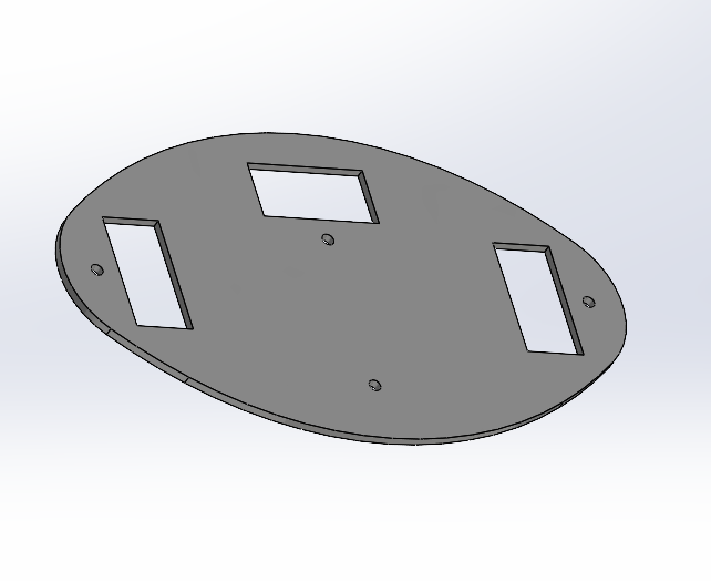
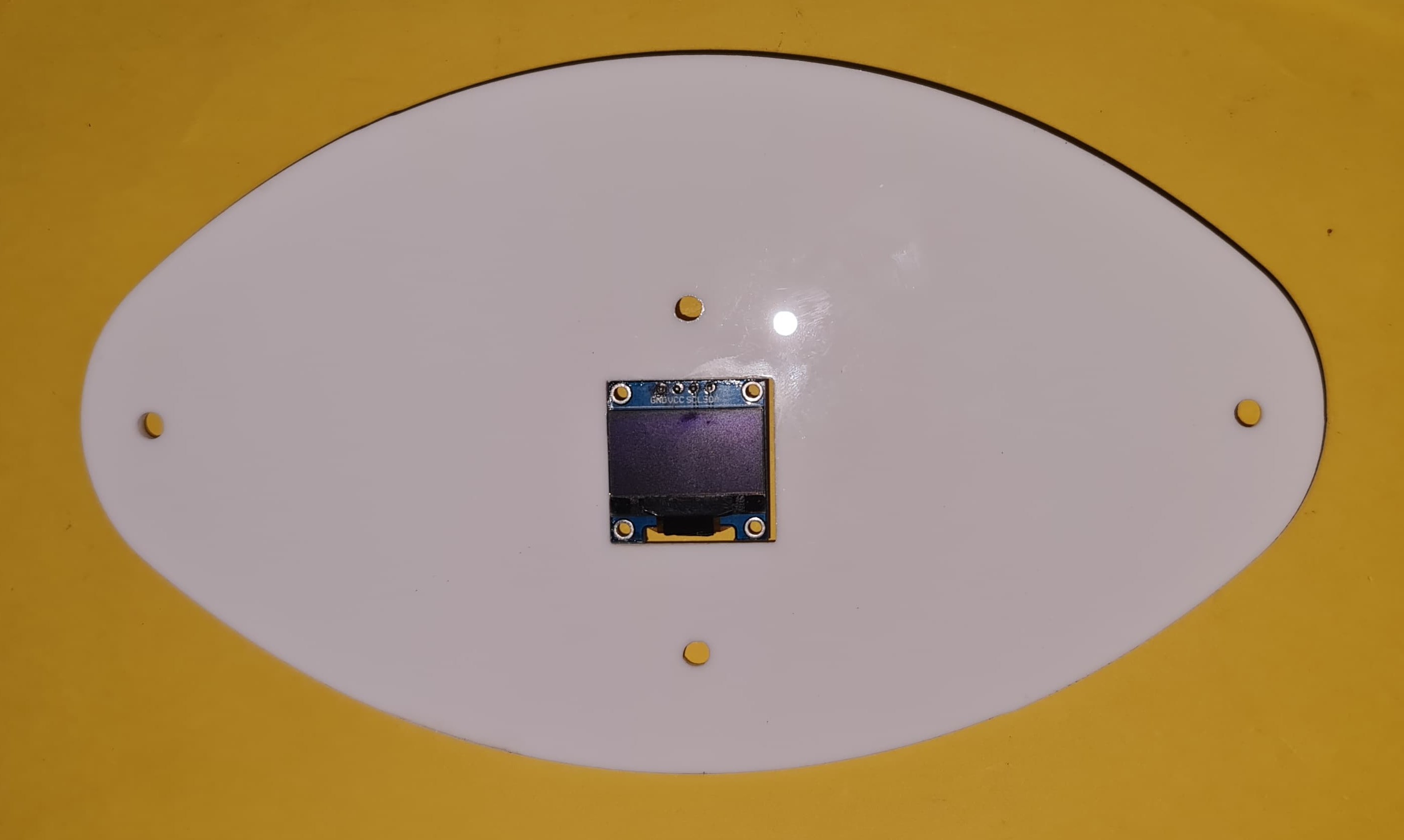
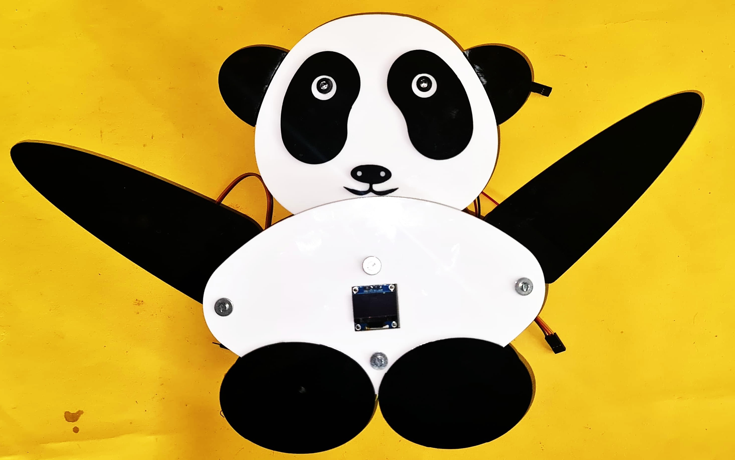
| OLED Fitted in front side of stomach part |
|
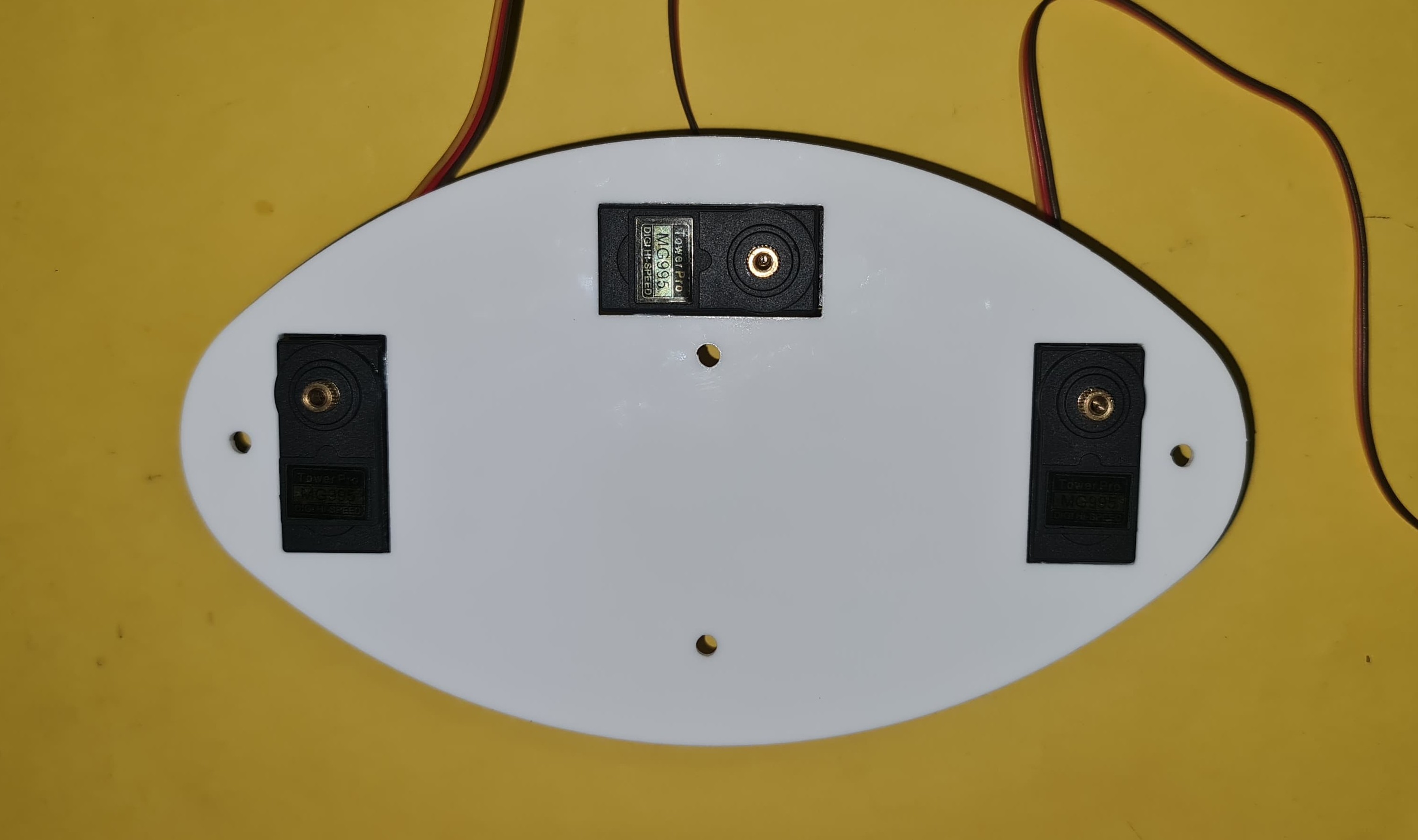
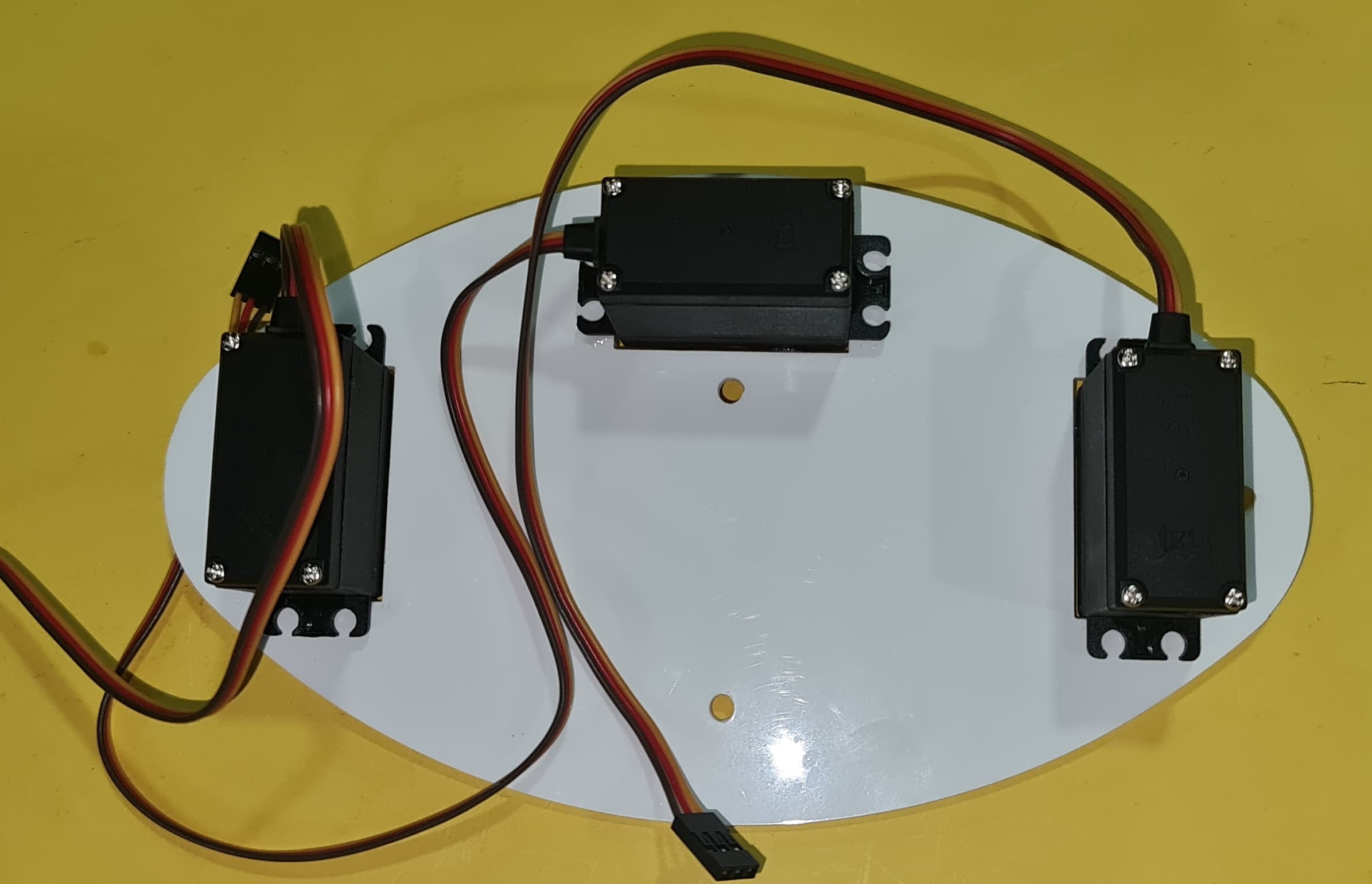
| Servo Motor Assembled on the Back Side of the Stomach |
|
| Back Side |
| Complete harwware part and 2 D part Assembling |
|
| All Components & Hardware parts fully assembled. |
Testing Hardware
Summary
In this assignment, I started by gathering all the hardware components required for my project and studied how each component works and is programmed. I then focused on understanding the complete working mechanism of the project. After that, I designed the PCB and used the SRM milling machine to cut it. Finally, I soldered all the components onto the PCB to complete the hardware setup.
Conclusion
This assignment taught me the value of proper planning and preparation before beginning a final project. By understanding the operation of each component and having a clear workflow, the entire process became more efficient and manageable. It also improved my skills in PCB design, milling, and hardware integration, giving me a strong foundation for completing my final project successfully.