Week 8
Electronics Production
Welcome to week eight. This week's focus is on the creation of electronics. I used KiCad to successfully learned about PCB layout designing during Electronics design Week. I started the fabrication process by generating the Gerber files, confirming the design guidelines, and exporting the layout after finishing the schematic and PCB routing steps. This signaled the change from design to practical hardware implementation.
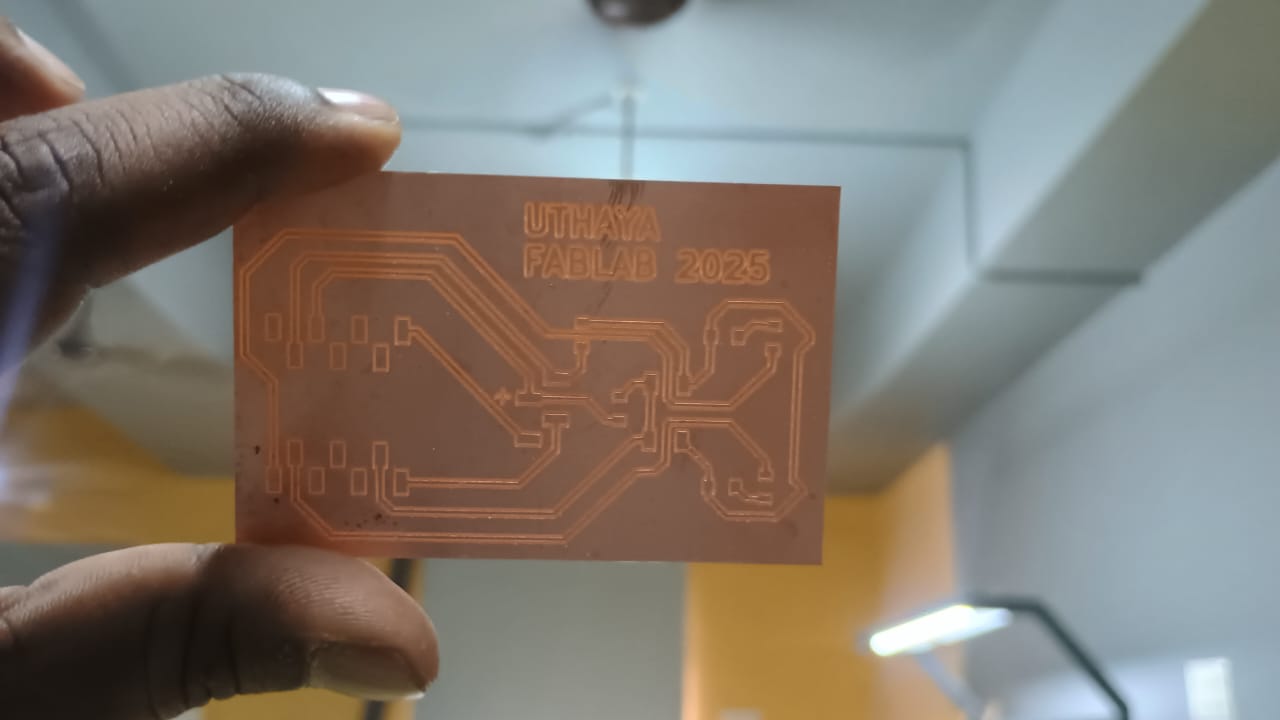
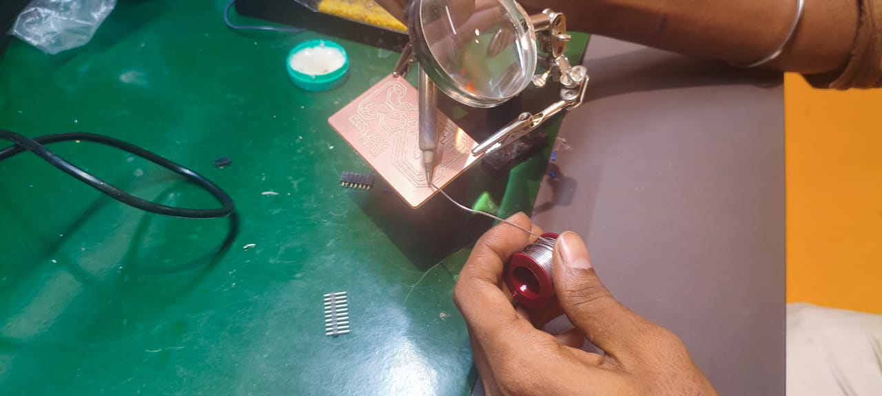
My Heroshot for this Week
 |
 |
Group assignment :
- Characterize the design rules for your in-house PCB production process: document feeds, speeds, plunge rate, depth of cut (traces and outline) and tooling.
- Document the workflow for sending a PCB to a boardhouse
- Document your work to the group work page and reflect on your individual page what you learned Click to open our Group Assignment
Individual assignment :
PCB Production :
In PCB production at fab labs, we employ the milling machining method, akin to printing on paper with a regular printer. The fab lab offers a Wegstr CNC machine. 3-axis milling machine for this purpose. This machine functions as a standard milling machine suitable for PCB fabrication
Outcomes
Group assignments:
Characterize the design rules for your in-house PCB production process: document feeds, speeds, plunge rate, depth of cut (traces and outline) and tooling.
Document the workflow for sending a PCB to a boardhouse
Document your work to the group work page and reflect on your individual page what you learned
Individual assignments:
Make and test a microcontroller development board that you designed
reference links


What is a Printed Circuit Board?
A printed circuit board (PCB) is an electronic assembly that uses copper conductors to create electrical connections between components. PCBs also provide mechanical support for electronic components so that a device can be mounted in an enclosure.
All PCBs are built from alternating layers of conductive copper with layers of electrically insulating material. Conductive features on printed circuit boards include copper traces, pads, and conductive planes. The mechanical structure is made up of the insulating material laminated between the layers of conductors. The overall structure is plated and covered with a non-conductive solder mask, and silk screen is printed on top of the solder mask to provide a legend for electronic components. After these fabrication steps are completed, the bare board is sent into printed circuit board assembly, where components are soldered to the board and the PCBA can be tested.
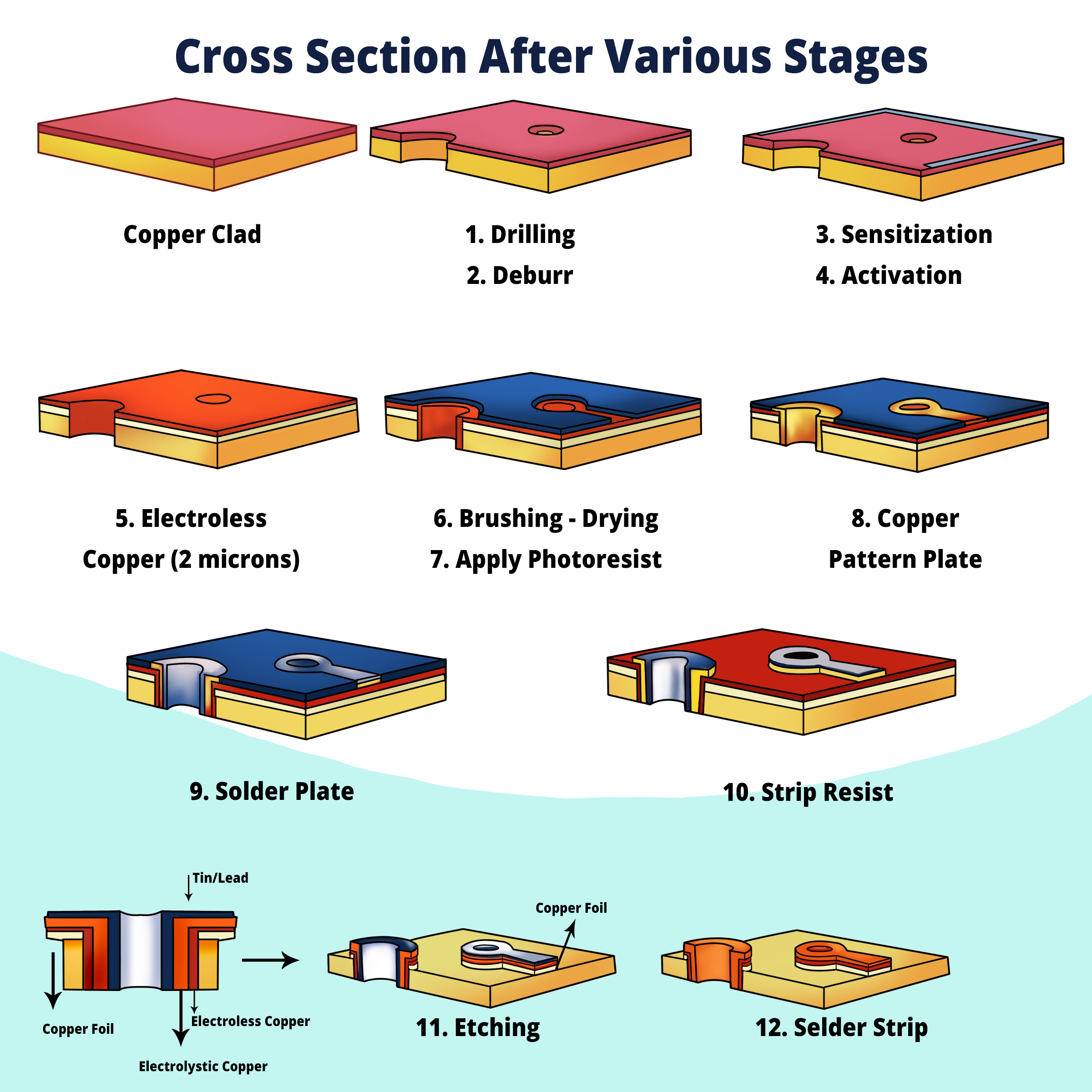
During manufacturing, the inner copper layers are etched, leaving the intended traces of copper for connecting components in the circuit board. Multiple etched layers are laminated in succession until the printed circuit board stack-up is complete. This is the overall process used in PCB design fabrication, where the bare board is formed before passing through a printed circuit board's assembly process.
Different types of PCBs :
Single-layer PCBs:
|
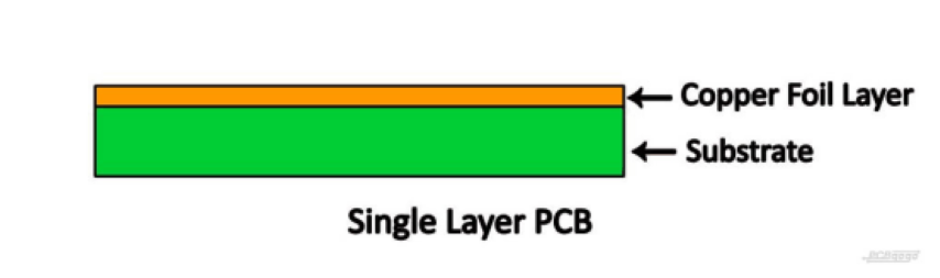 |
Double-layer PCBs:
|
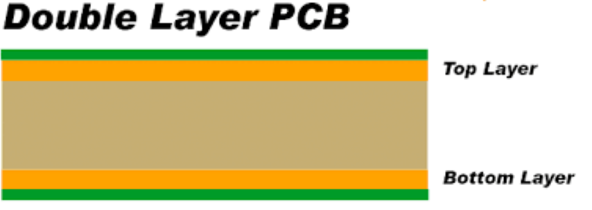 |
Multi-layer PCBs:
|
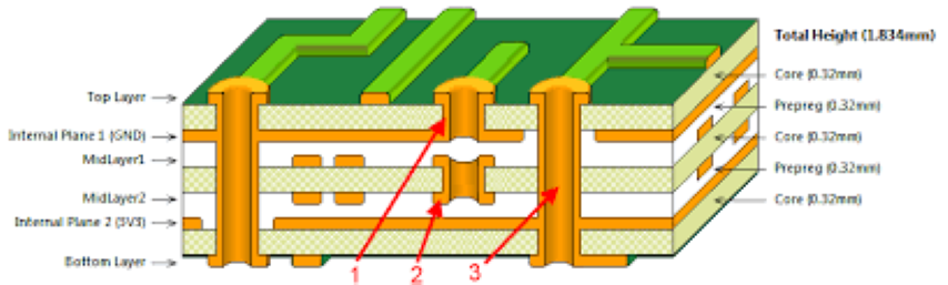 |
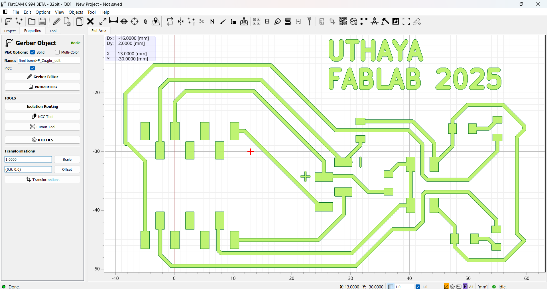
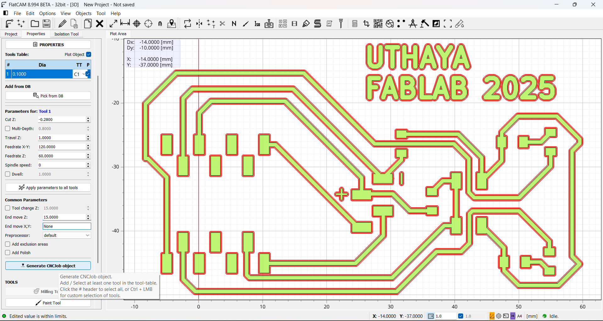
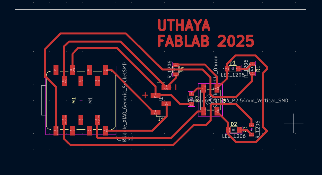
I have designed a pcb layout using kicad
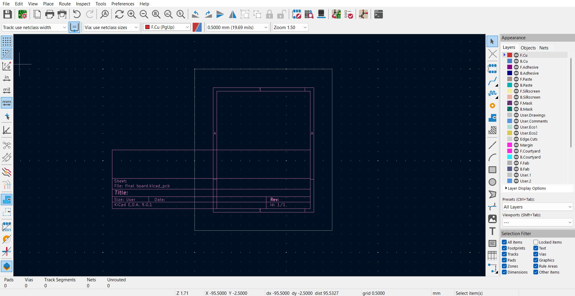
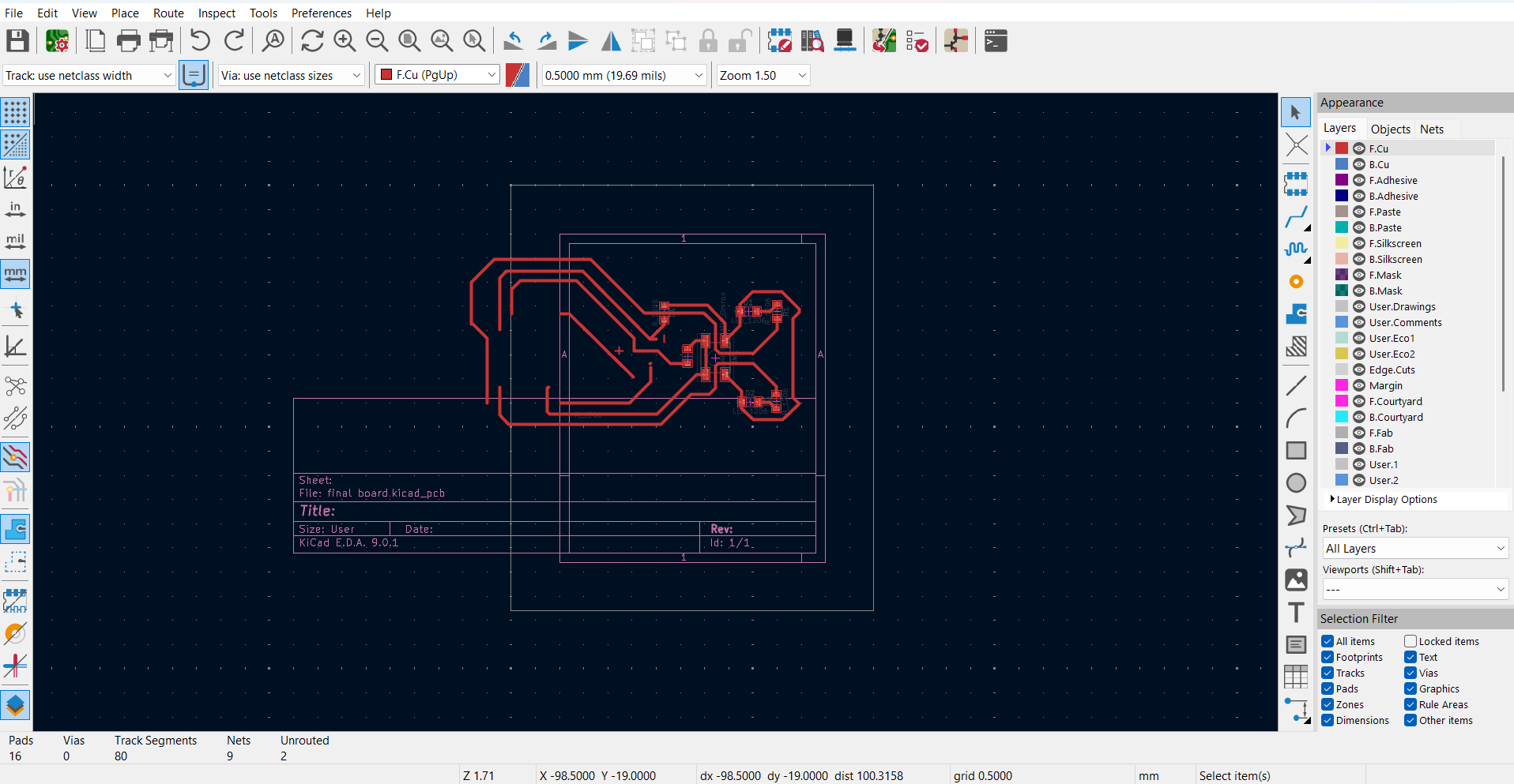
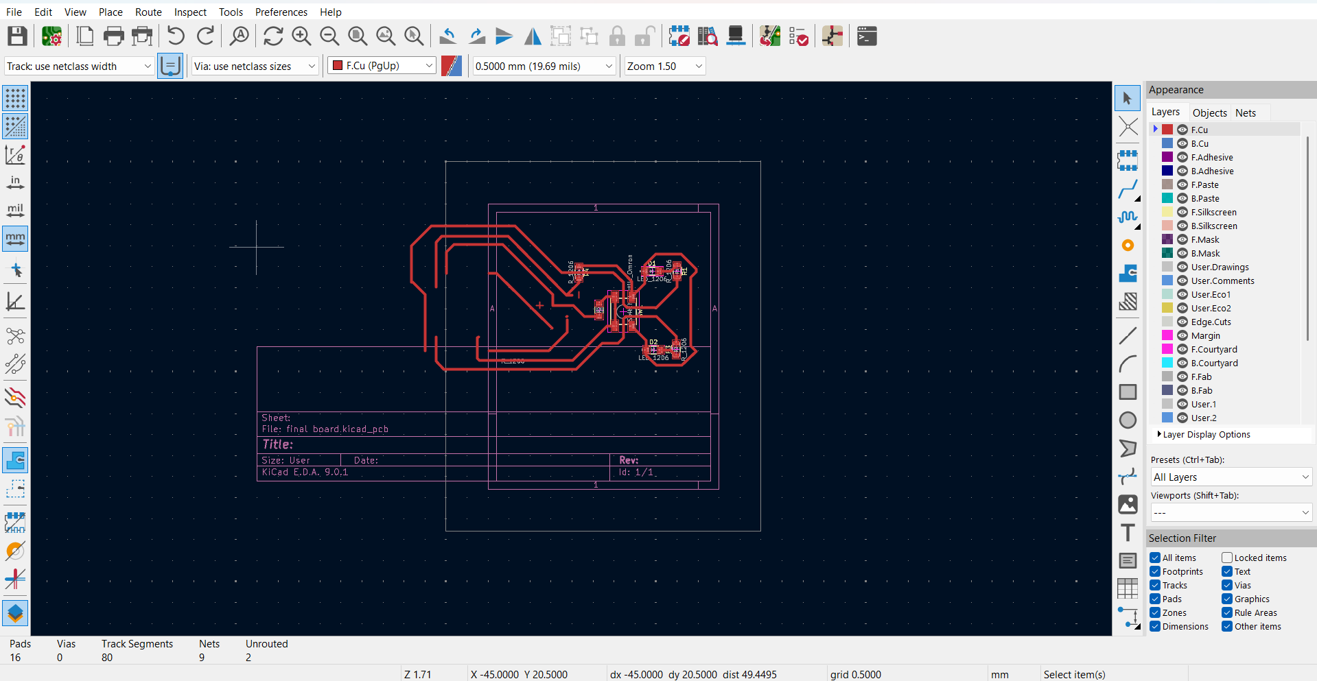
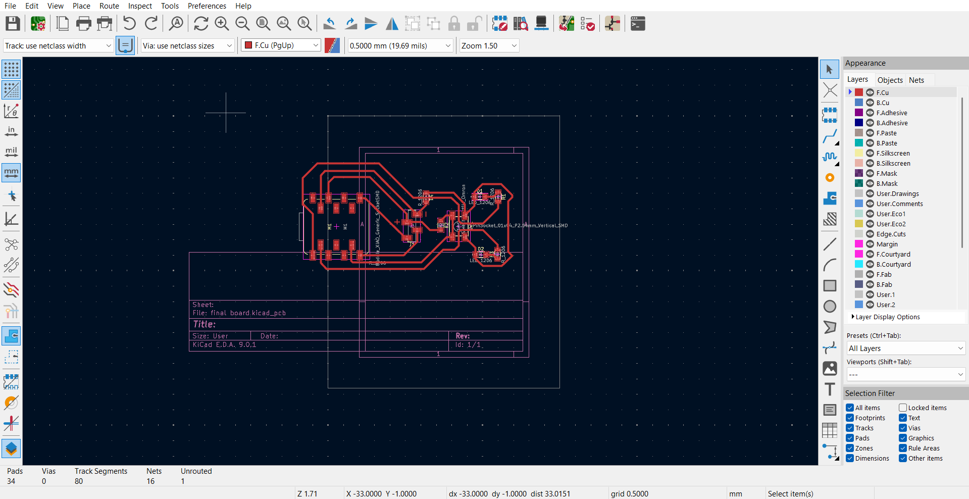
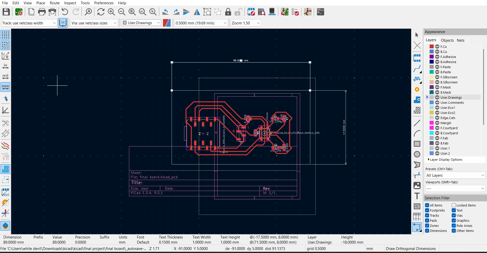
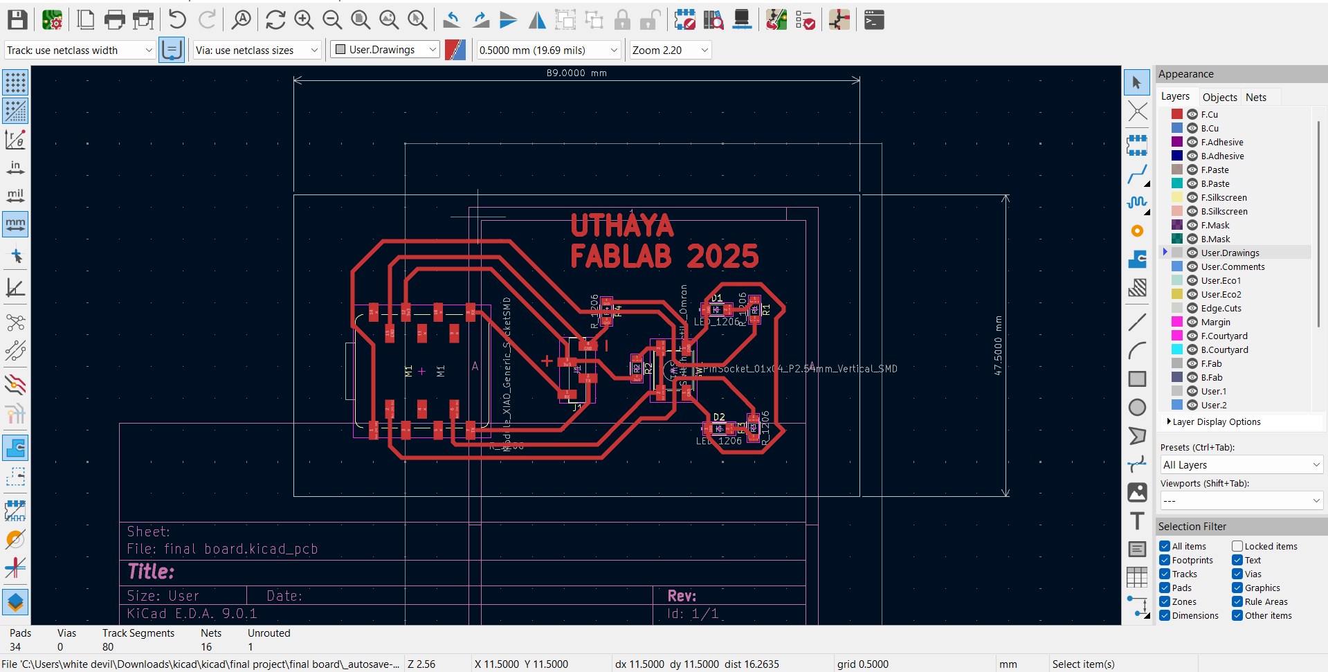
Final design :
Preparation for milling :
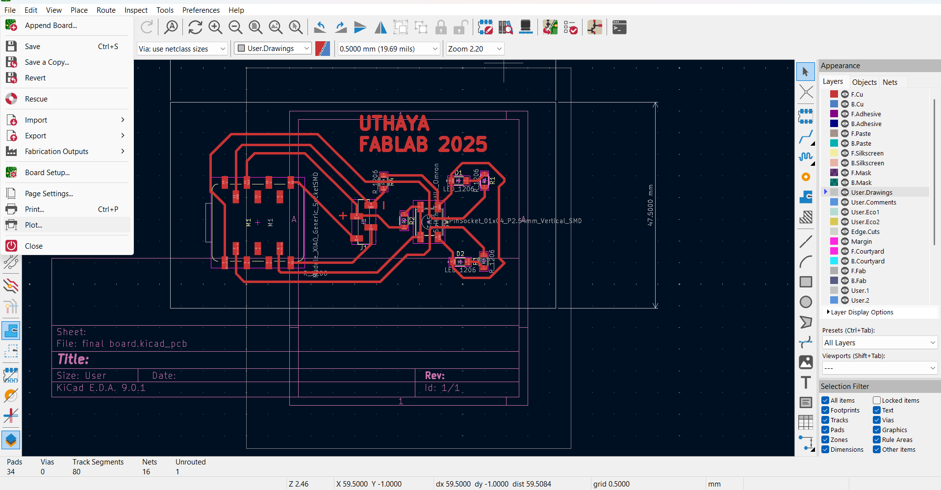
To create the required output files, I went to the "File" menu in the PCB Editor and chose the "Plot" option. In order to prepare the Gerber files for PCB manufacture, this step is crucial. Before starting the plot, I made sure the right layers were chosen.
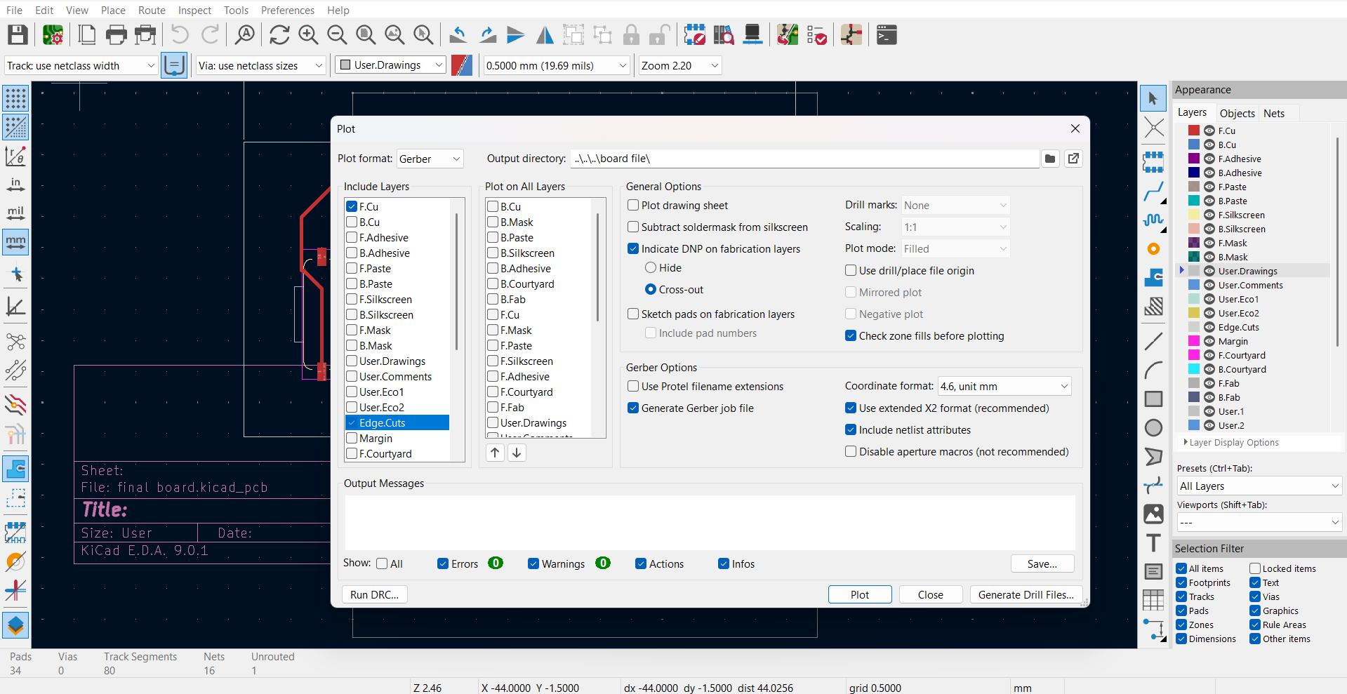
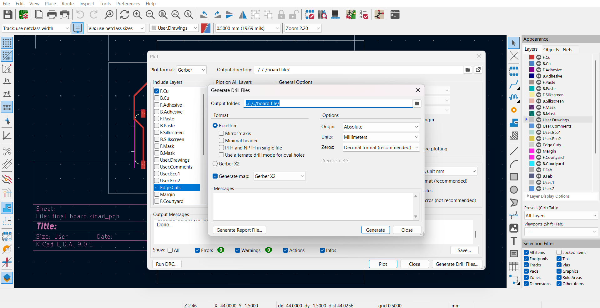
I created the Gerber files—which are necessary for PCB fabrication—in the PCB Editor's Plot feature. I choose the required layers, including Edge and F.Cu.cuts that made sure all pertinent information was incorporated for precise production results.
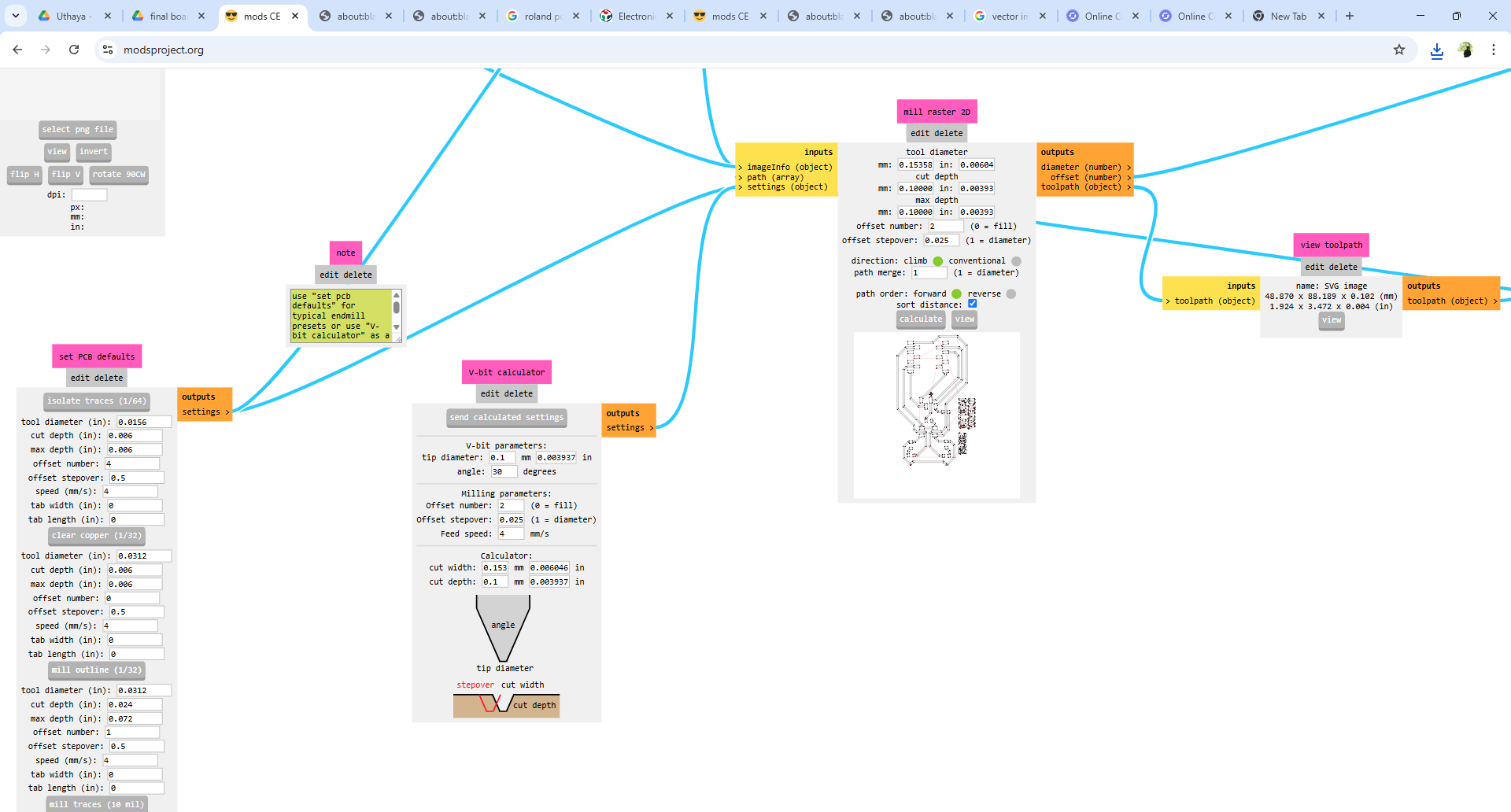
Introduction to FlatCAM :
An open-source program called FlatCAM is used to translate drill and Gerber files into G-code, which is necessary for PCB milling with CNC equipment. Because it enables users to build board outlines, drill patterns, and isolation pathways, it is very helpful in PCB prototyping. Tool diameter, cut depth, feed rate, and other customization options are available with FlatCAM, which allows a variety of CNC milling processes. It makes it simple to get PCBs ready for manufacture without the need for chemical etching by giving a visual representation of tool paths.
FlatCAM Home Page Overview :
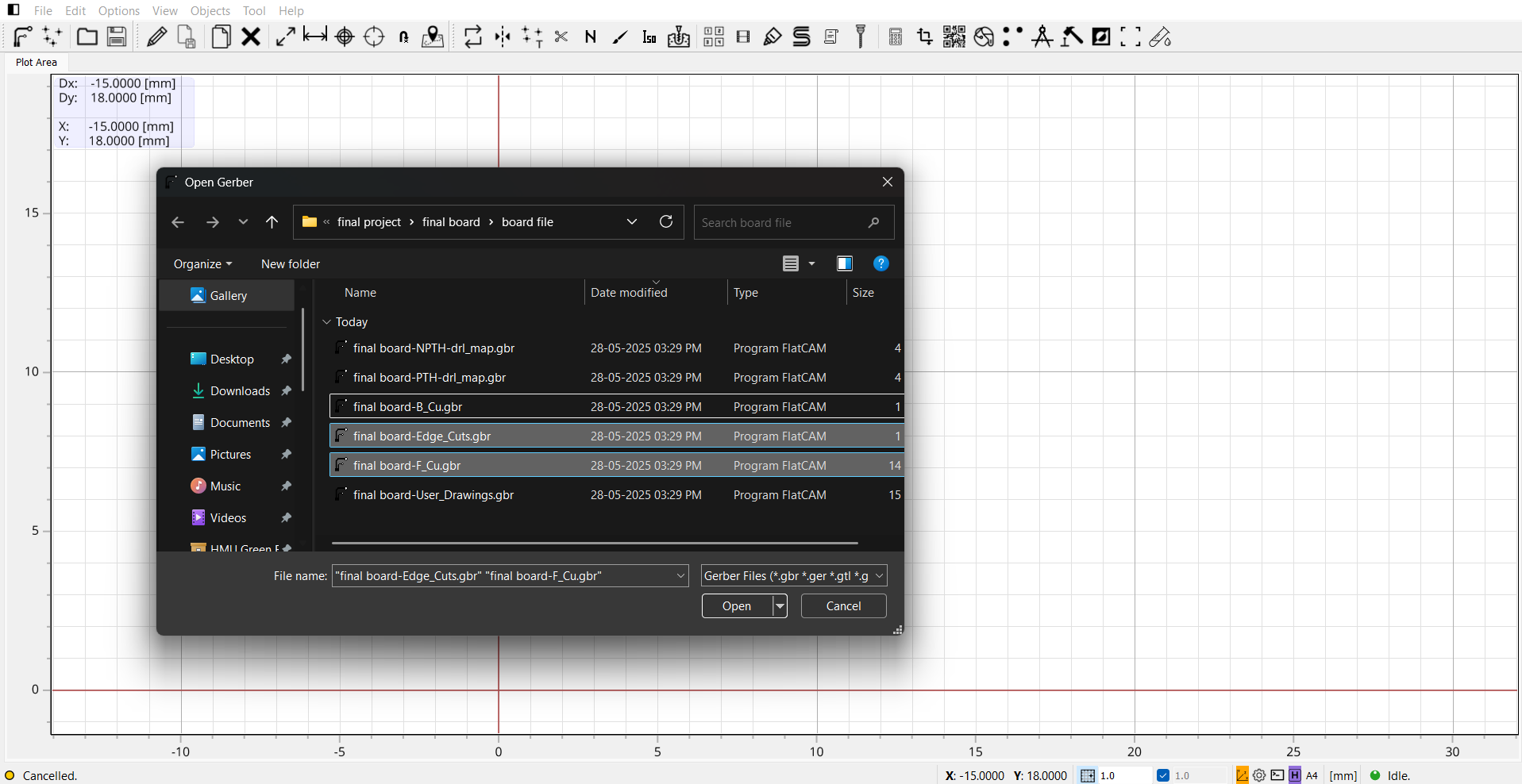
In FlatCAM, import the F.Cu and Edge.Cuts Gerber files by selecting “File → Open Gerber.” Load the top copper layer (F.Cu) and the board outline (Edge.Cuts). Both layers will appear on the canvas and project panel. Ensure alignment before proceeding with further PCB fabrication steps like isolation routing.
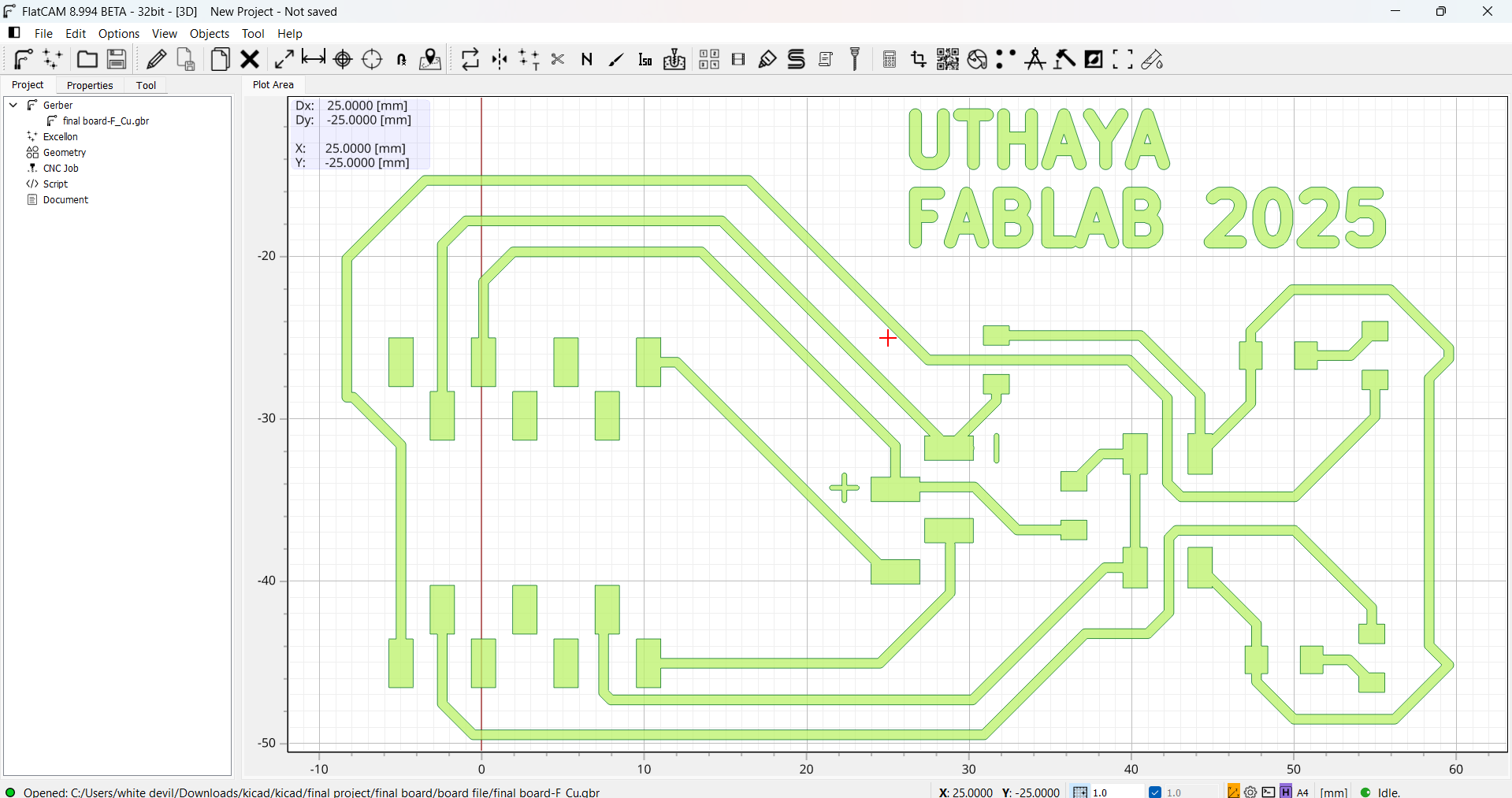
After importing the F.Cu and Edge.Cuts files in FlatCAM, the layout appeared off-screen. To fix this, I realigned the design to the origin using the "Align Origin" tool. This ensured the copper traces and board outline were correctly positioned for accurate toolpath generation and smooth PCB fabrication.
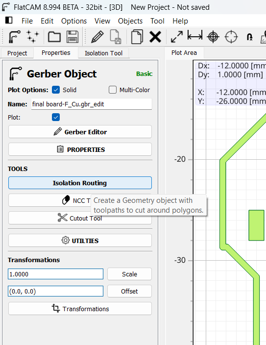
I then choose the Isolation Tool in FlatCAM's Properties menu. In order to ensure clean traces and specify how the copper will be isolated from the board, this step is essential.
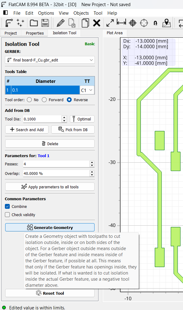
I then looked at the available milling bits and their characteristics in FlatCAM's Tool Database. This made sure that, depending on the PCB material, I chose the appropriate tool diameter, cut depth, and feed rate.
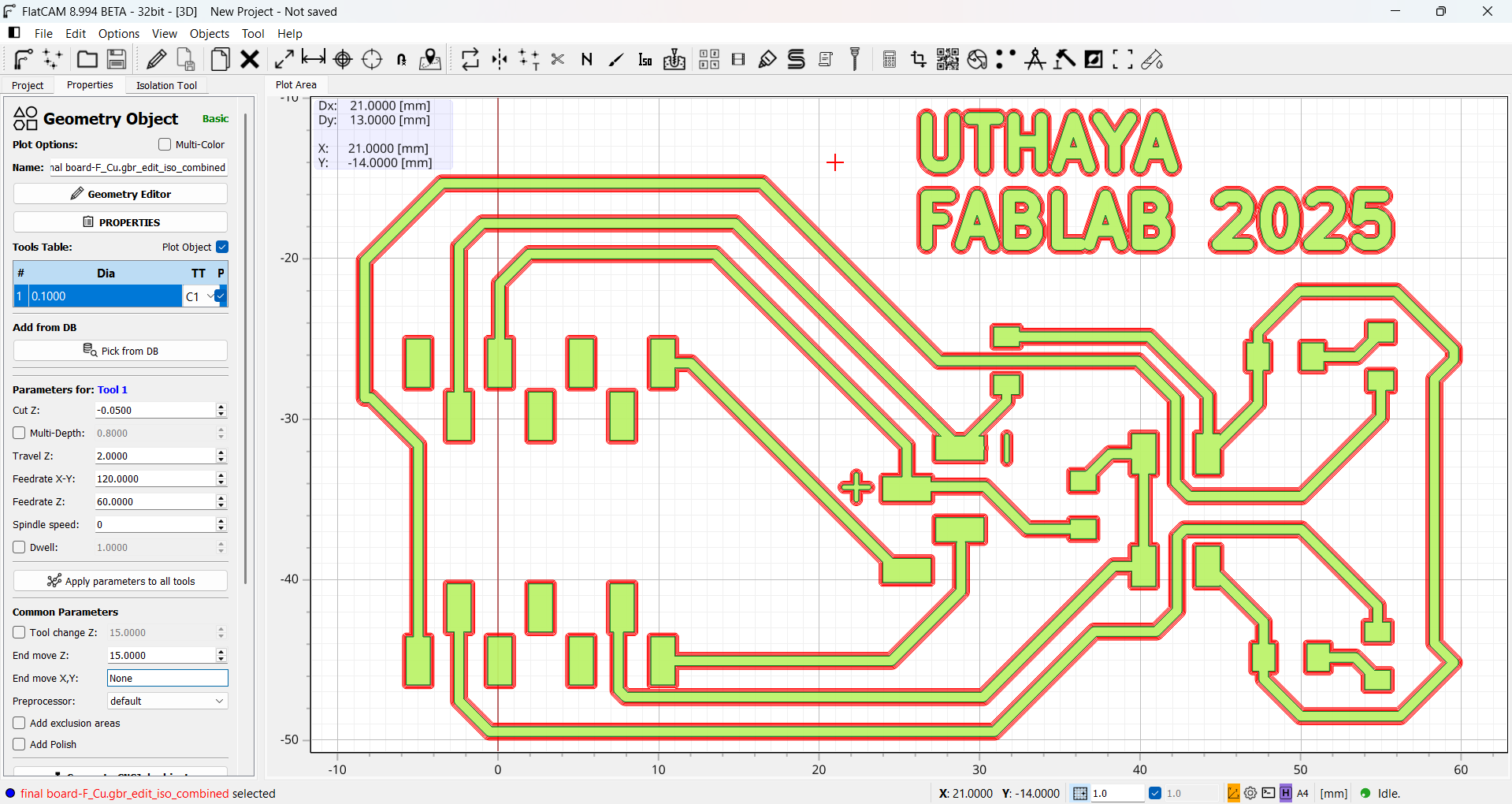
I had to manually generate the necessary tool settings because FlatCAM does not come with a preloaded Tool Database. I created the geometry by setting important parameters including feed rate, spindle speed, cut depth, and tool diameter. These numbers were selected in accordance with the end mill specifications and my PCB requirements.
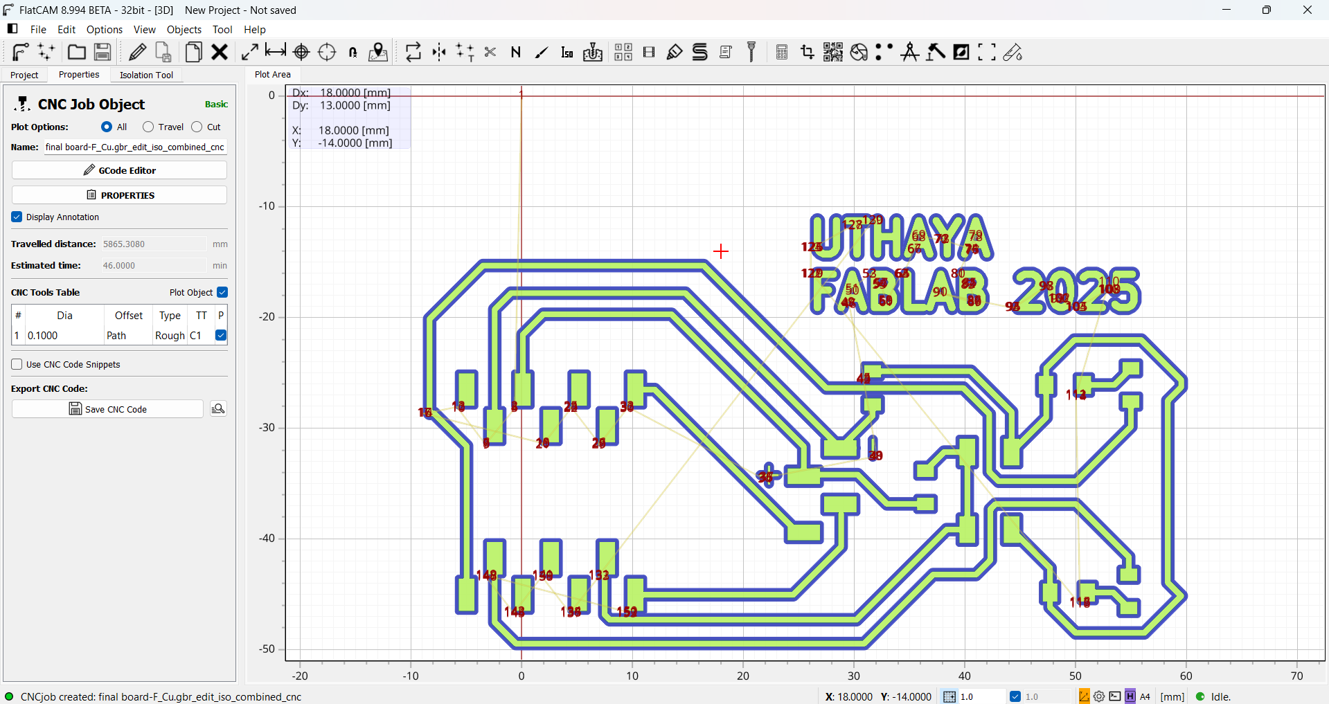
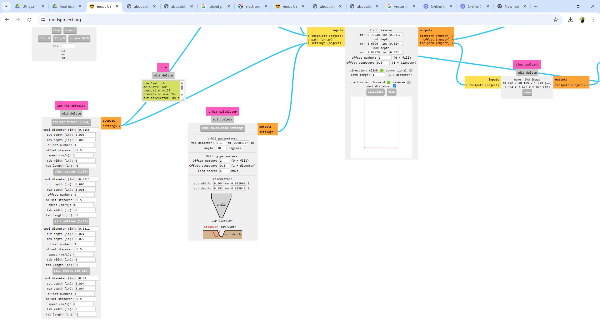
After creating the Edge Cut path, I looked at the CNC code (G-code) that was produced for the milling operation. The precise tool movements, depths, and coordinates needed by the CNC machine to precisely cut the board outline are included in this code.
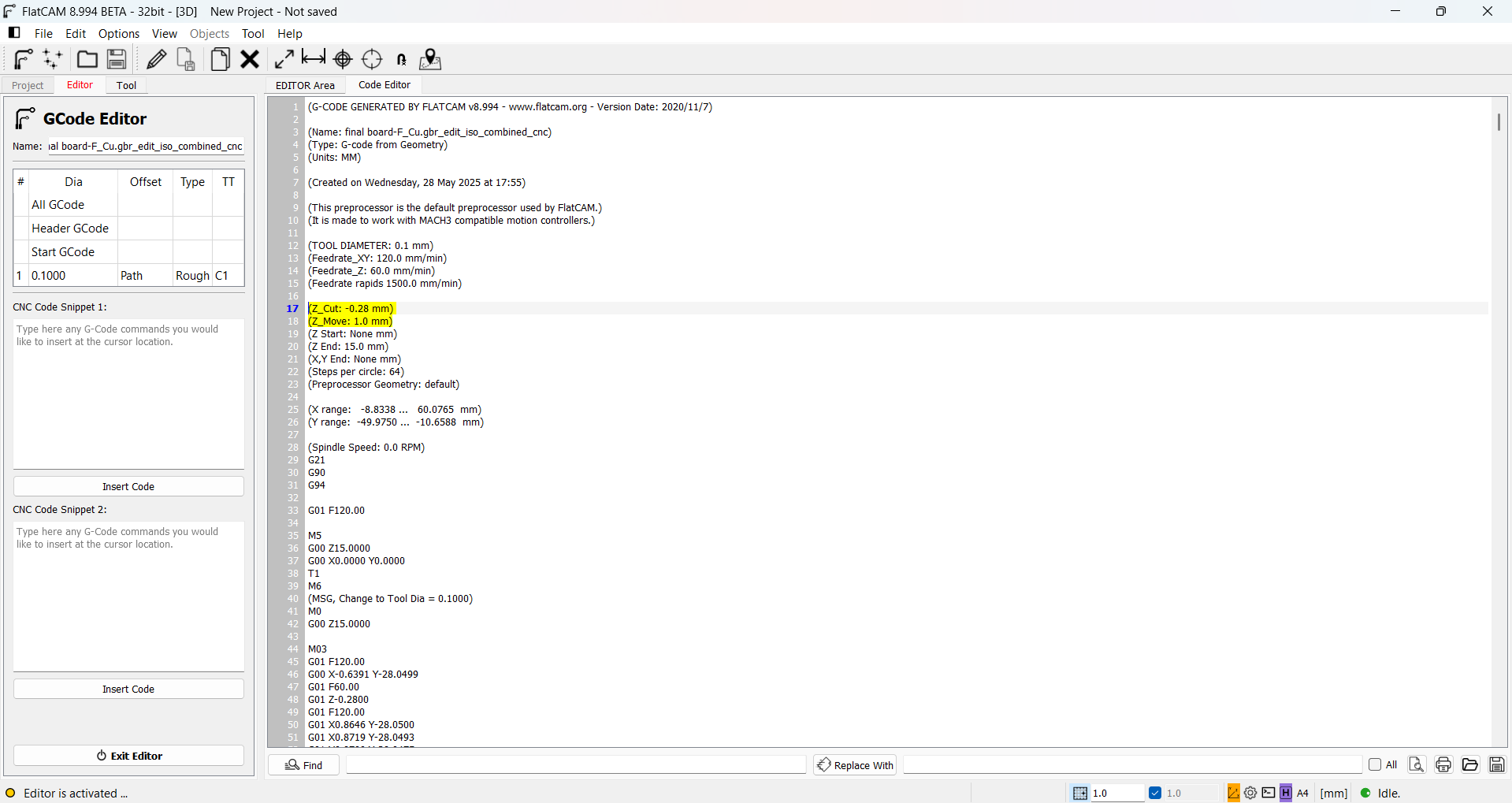
Verifying the CNC code guarantees that all coordinates, cut depths, and tool trajectories are specified accurately. In order to prevent fabrication problems like inaccurate measurements or tool collisions, this step is essential. Additionally, it ensures a smooth milling process by confirming that the PCB outline, traces, and holes match the original design.
I double-clicked the Gerber item in FlatCAM, then went to the 'Cutout Tool' area to create the PCB outline's rectangle geometry. I adjusted the necessary tool parameters and margins in this stage to guarantee that the cutout path that was produced was exactly in line with the edge of the PCB for perfect board milling.
I therefore used the specified cutout shape to generate the CNC code. Toolpaths, spindle speed, and movement directives are among the many instructions required for the CNC milling machine that are contained in this code.
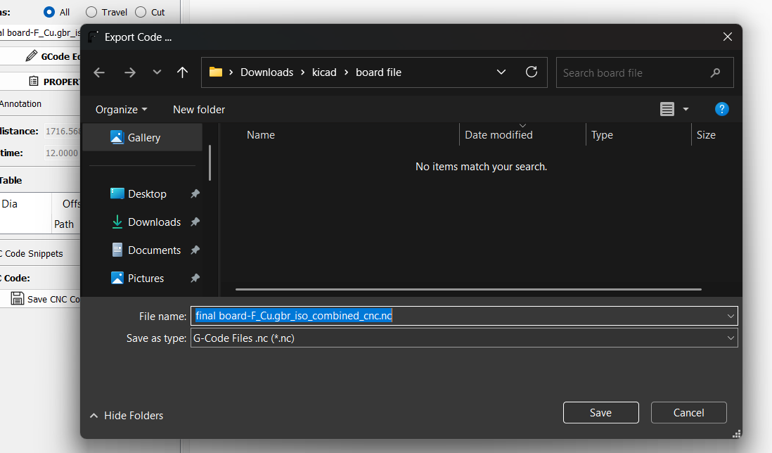
I carefully saved the CNC job file after creating the CNC code. All of the comprehensive instructions needed for the CNC machine to precisely grind the PCB are included in this saved file. The CNC task can be easily retrieved and used throughout the actual fabrication process if it is preserved.
I selected a handy spot on my PC to store the file after saving the CNC work. Later on during fabrication, I can easily obtain the CNC instructions thanks to this organization.
I used the same procedure for the front copper layer (F.Cu). I saved the CNC job for the F.Cu toolpath to a handy spot on my PC when it was generated.
reference files :
PCB Milling :
PCB milling is the process of mechanically removing material from a copper-clad board in order to construct circuit designs and establish electrical isolation. In contrast to conventional etching techniques, which dissolve undesirable copper using chemical solutions, milling physically removes the desired traces using precisely calibrated milling bits. A Computer Numerical Control (CNC) milling machine is usually used for the procedure; it is programmed to adhere to a certain design layout in order to ensure precision and reproducibility.
PCB Milling Machine :
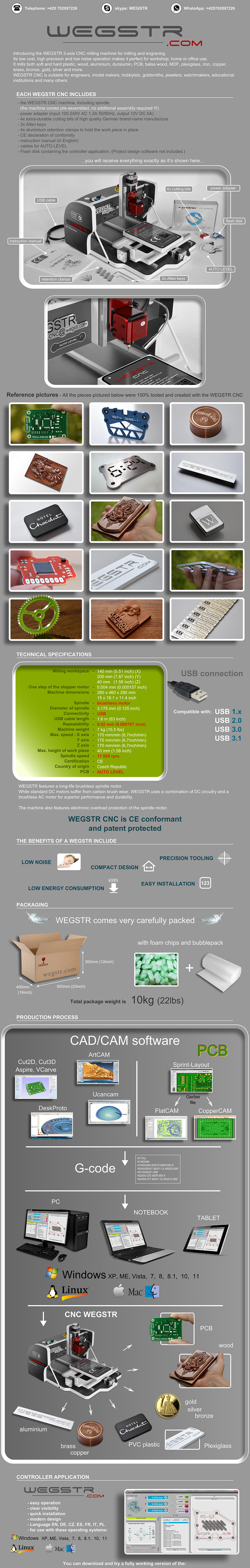
Introduction about Wegstr Machine and Software:
A small desktop CNC machine made especially for quick PCB prototyping is the Wegstr PCB milling machine. Instead of using conventional chemical etching, it enables customers to build circuit boards by milling copper-clad boards. For engineers, makers, and students who wish to rapidly test their circuit ideas, this is perfect. By offering an easy-to-use interface for loading, simulating, and controlling the CNC toolpaths (often in G-code format), Wegstr software enhances the machine. Users can configure spindle speeds, precisely control axis motions, observe the milling process, and import files created by FlatCAM (such as the front copper and edge cuts). The Wegstr machine and software work together to produce unique PCBs from your digital designs in a quick, clean, and environmentally responsible manner.
Our Machine Specification :
Our Tool Bits :
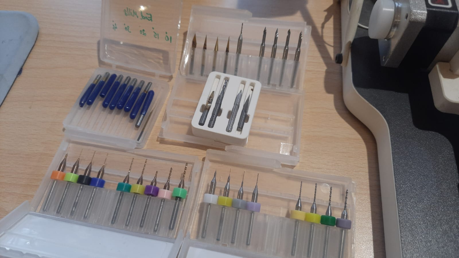
PCB milling bits are precision cutting instruments used to drill, cut, and engrave printed circuit boards (PCBs) in CNC milling machines. Each of these bits' different sizes and shapes is intended for a particular task, such as edge cutting, hole drilling, or trace isolation. End mills, V-bits, and engraving bits are common varieties.
- For the purpose of separating copper traces, engraving bits are utilized.
- For drilling and cutting board outlines, end mills are perfect solutions.
- V-Bits: Offer crisp and precise traces for detailed information.
- For durability, tungsten carbide is typically used as the material. Trace width, depth, board material, and necessary precision all influence bit choice.
Auto Levelling :
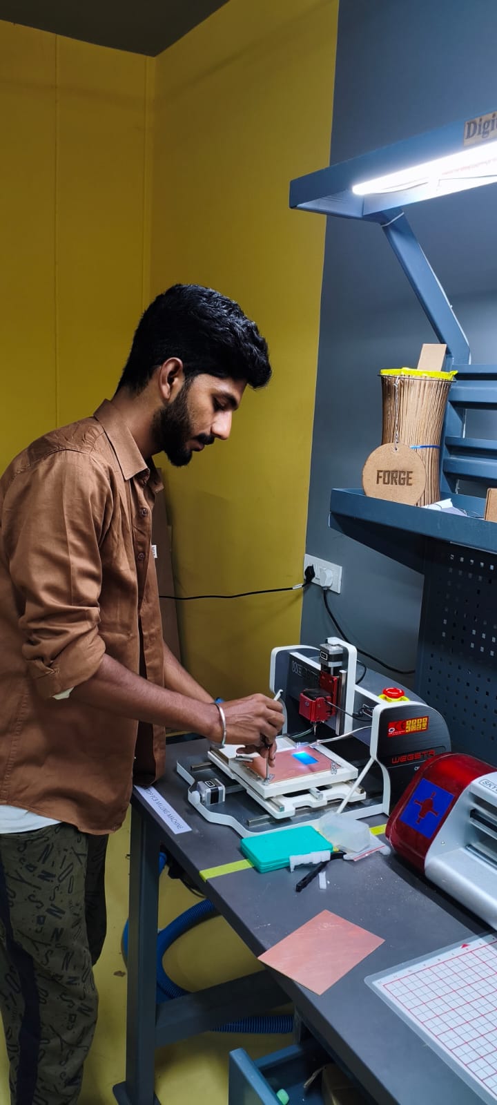
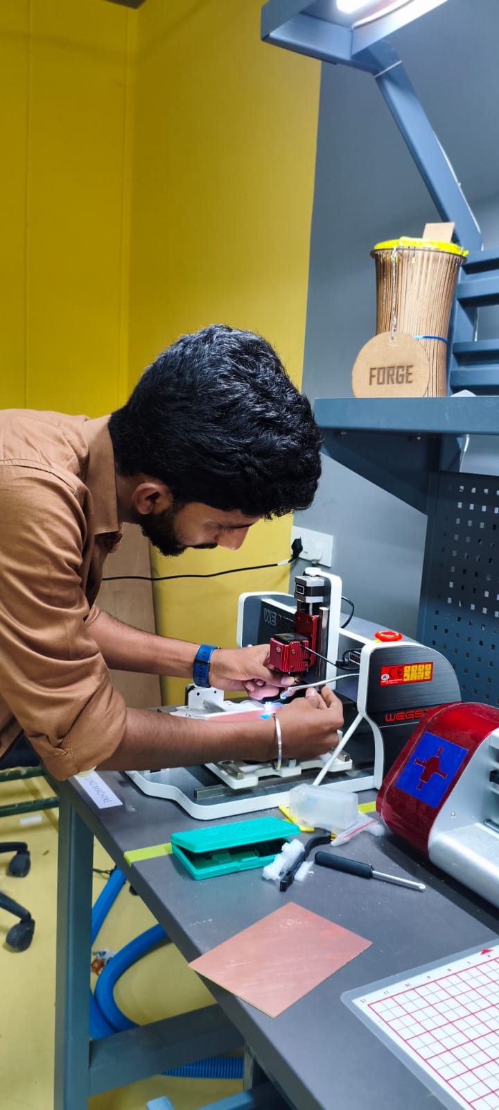
I set up the PCB milling machine for fabrication by connecting it to the computer. In order to guarantee stability while milling, I used the appropriate fittings to firmly fasten the copper-clad board onto the machine's bed. For perfect cutting and exact trace isolation throughout the milling process, this alignment is essential to preventing shifting.
To make sure the milling bit would maintain precise depth across the PCB surface, I manually checked the machine's auto-leveling. To ensure accurate engraving during the PCB construction process, I carefully set the Z-axis zero position by lowering the bit until it barely brushed the copper surface.
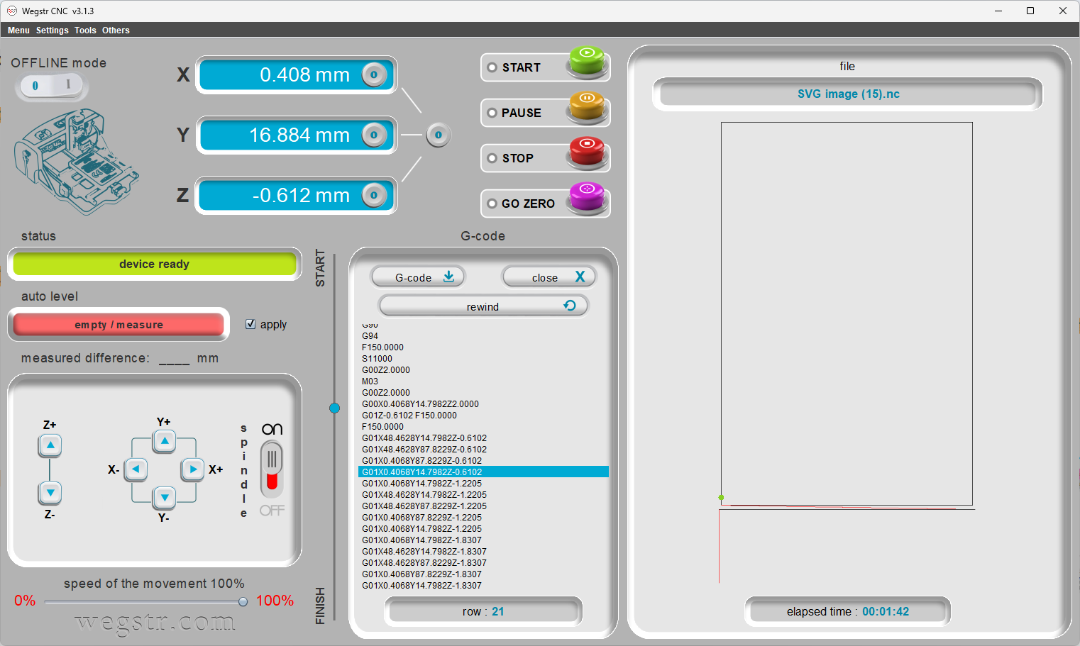
In order to confirm auto-leveling at every test point, I then loaded the F.Cu (front copper) file into the Wegstr program. By minimizing uneven milling and guaranteeing that the copper surface is consistently leveled and aligned with the toolpath, this step enhances the precision and caliber of the PCB engraving throughout production.
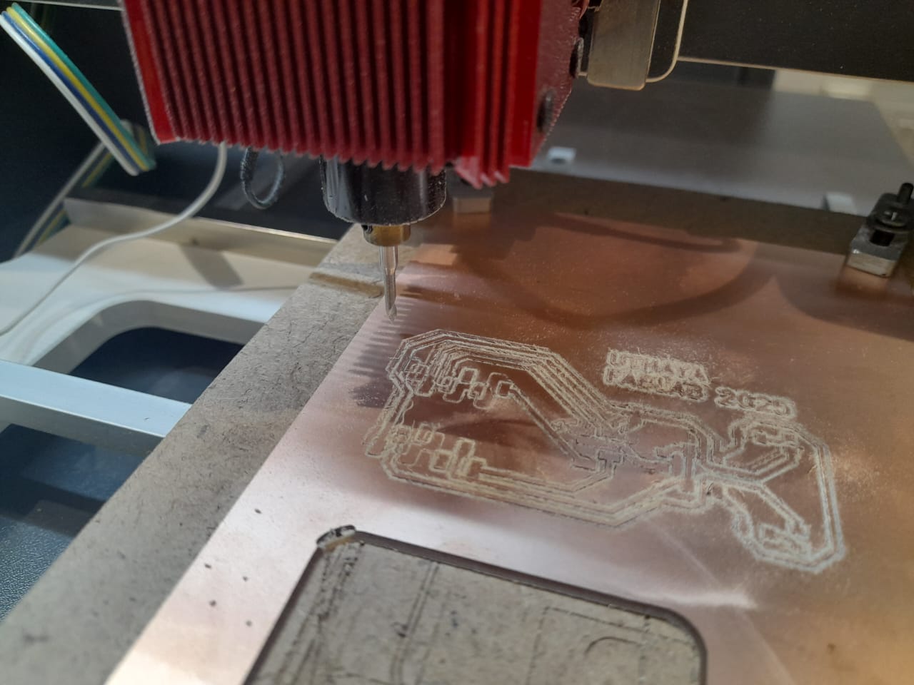
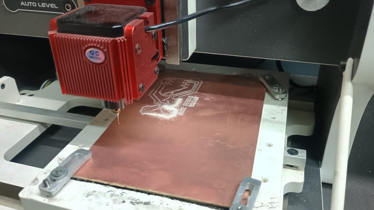
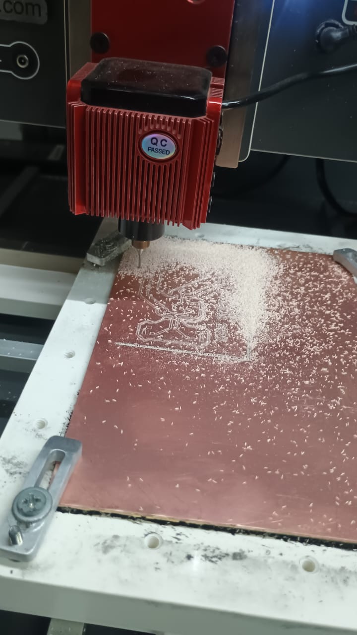
Milling Operation :
I started the Wegstr machine's milling operations after finishing the auto-leveling procedure. The spindle ensured accurate cuts for the front copper traces by adhering to the modified toolpaths depending on the auto-leveled surface.
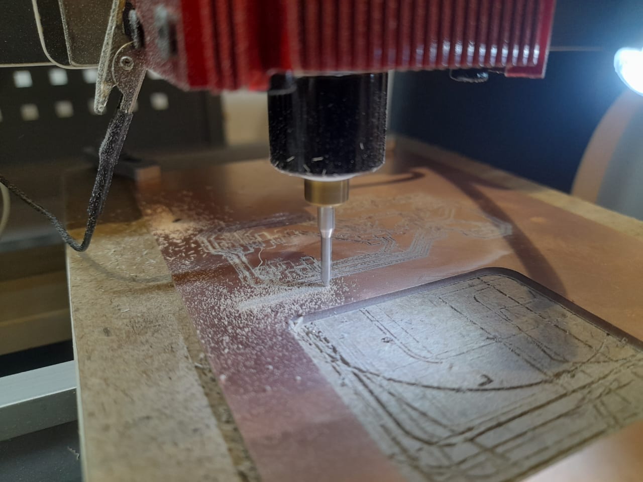
As specified by the NC (Numerical Control) code, the spindle moved along the X and Y axes while rotating at 11,000 RPM during the milling operation. As soon as the milling operation was complete, the software automatically notified completion. The final milled PCB output, shown above, shows that the toolpath instructions were successfully executed.
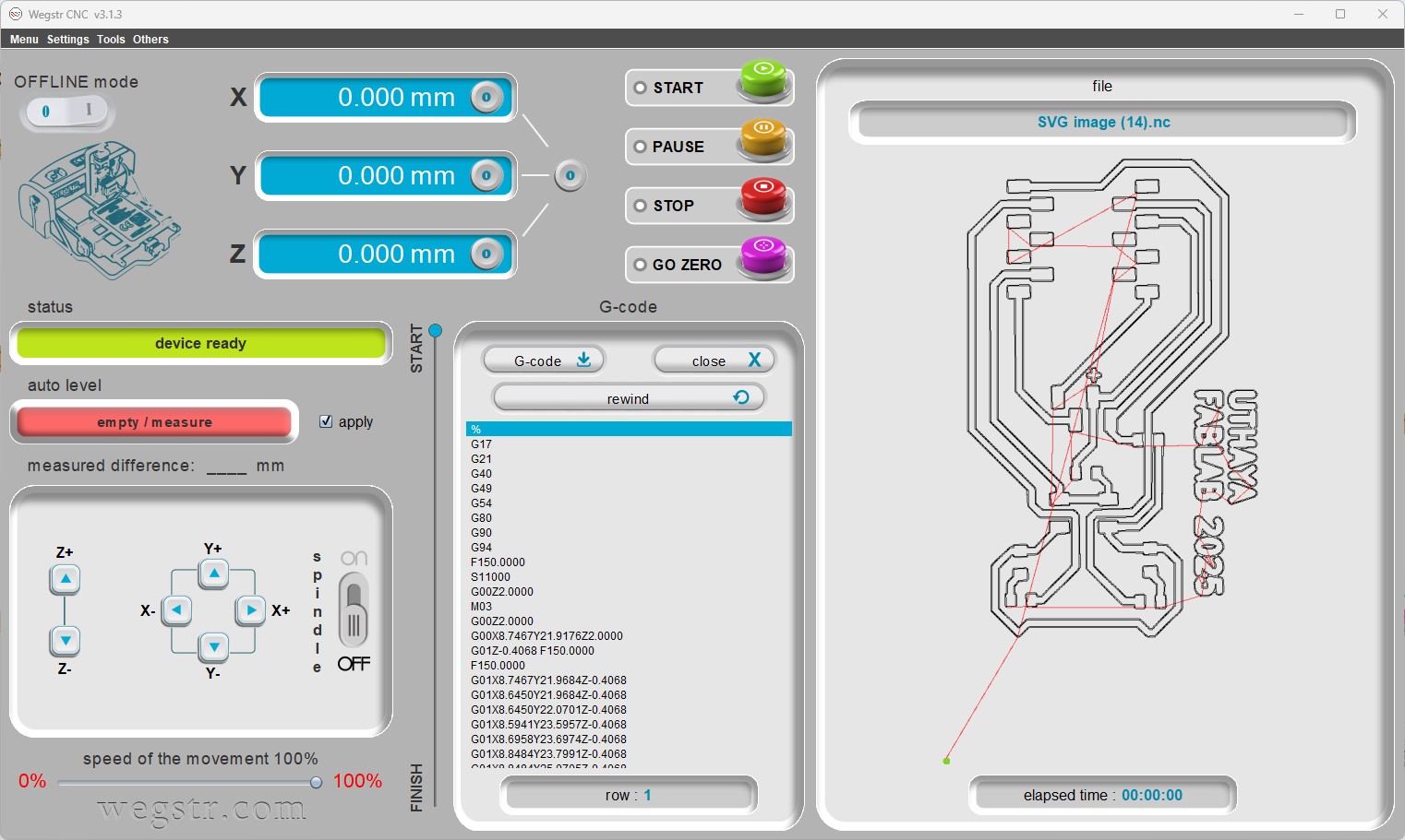
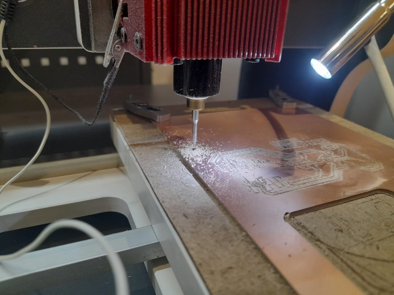
The edge cut file was then imported into the Wegstr program. I used the preview option to check the file after import to make sure the alignment and toolpath accuracy were correct. After making sure, I started the edge cutting process, which enabled the machine to accurately cut out the PCB board outline according to the design.
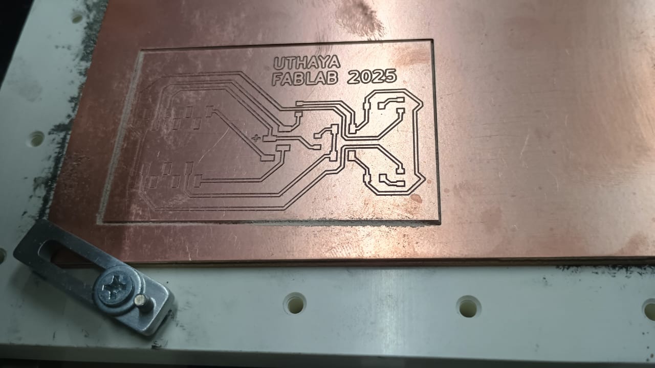
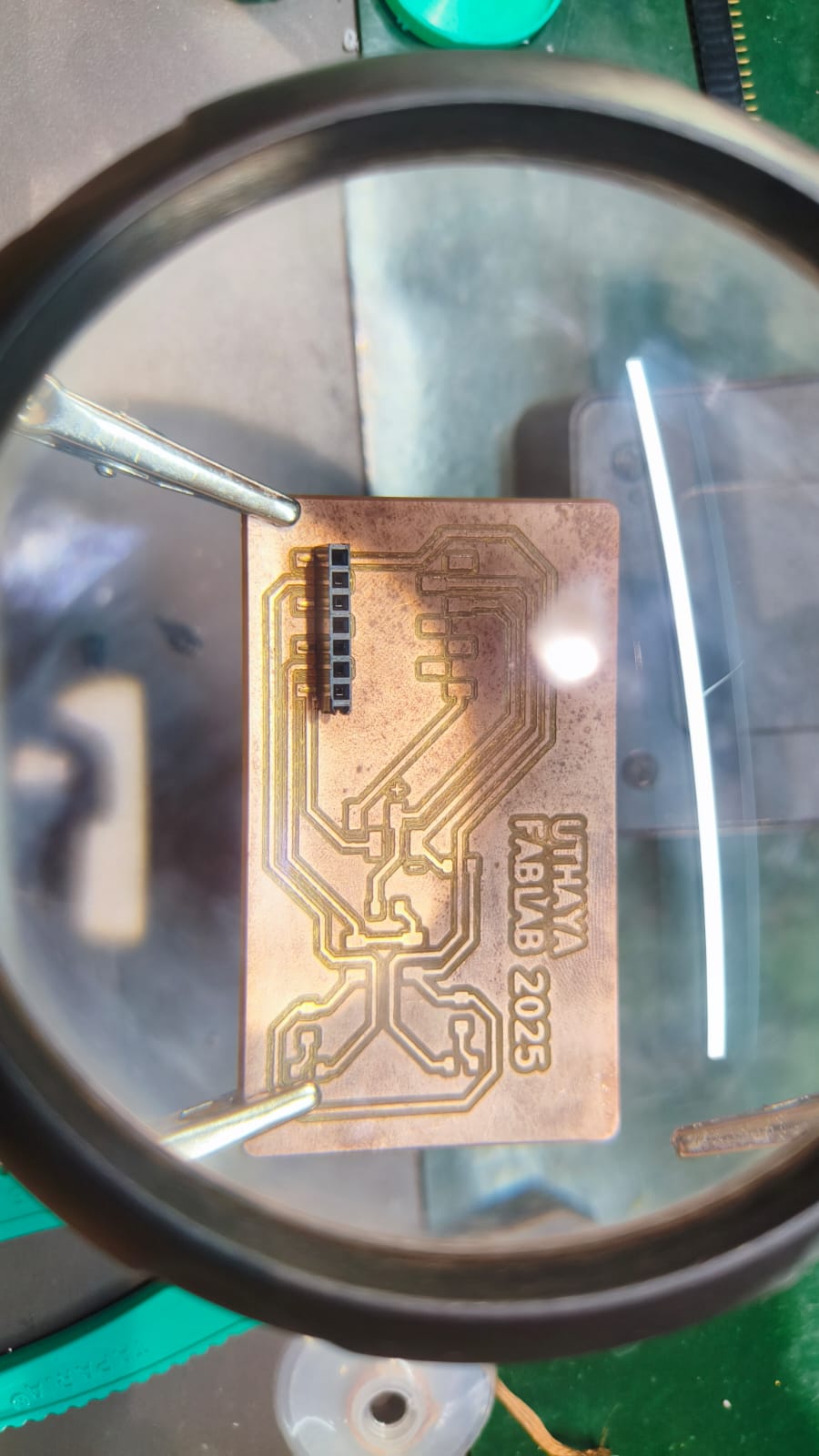
The machine completed the edge cut milling.
Final output:
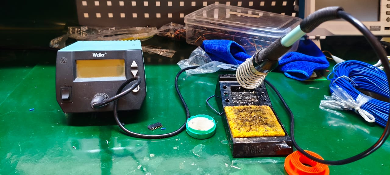
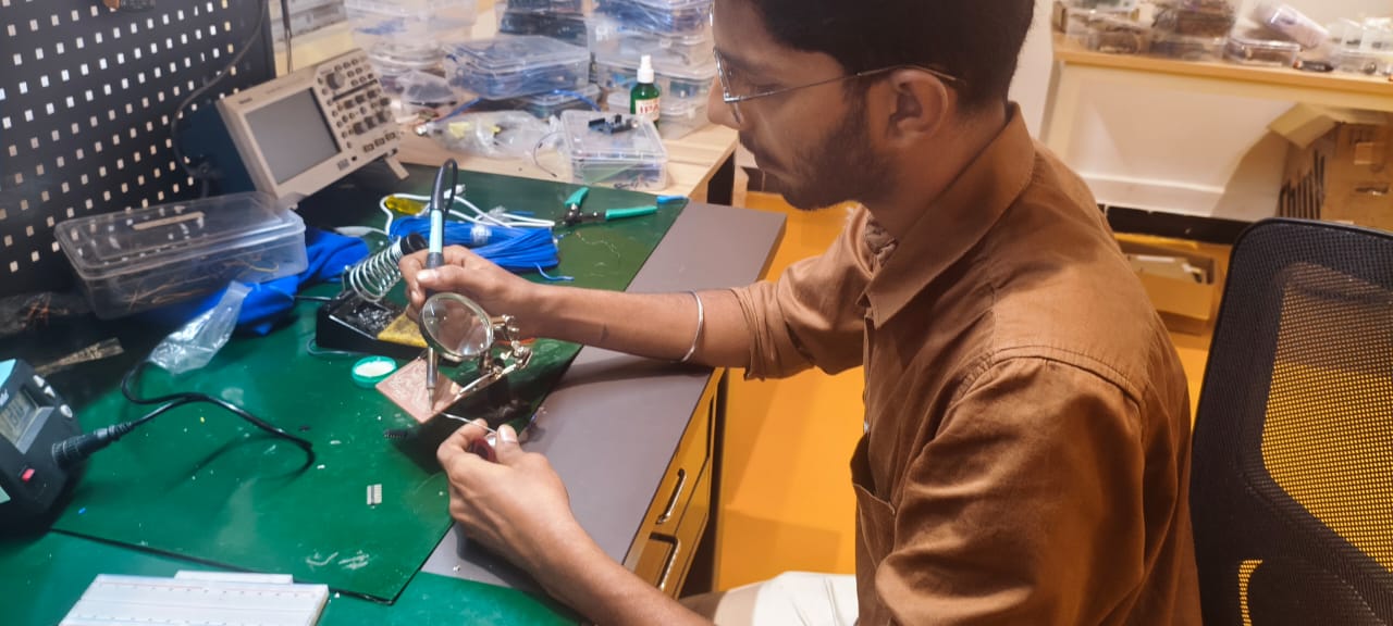
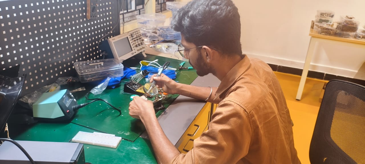
Soldering :
Soldering is the technique of melting and pouring a filler metal (solder) into a joint to fuse two or more metal components together. A bond can be formed without melting the base metals because the filler metal, which is usually in the form of an alloy or wire, has a lower melting temperature than the materials being joined. Soldering is frequently used to make solid and long-lasting connections between components in a variety of industries, including electronics, plumbing, metalworking, and jewelry creation. The solder must be melted by heating the junction to the proper temperature using a soldering iron or soldering gun.
Safety precautions for soldering:
- Make sure the workspace has enough ventilation to avoid breathing in the potentially dangerous fumes released by solder and flux. To help with ventilation, use fume extractors (fans) or work close to an open window.
- If you're working in a poorly ventilated area, wear a mask to protect yourself from inhaling harmful fumes.
- Keep your fingers away from the soldering iron's heat by using instruments like clamps or tweezers to hold components in place.
- Always return the soldering iron to its stand when not in use, and never leave it unattended while it's still hot to prevent accidents.
- After soldering, wash your hands thoroughly to remove any residue and prevent accidental ingestion of harmful substances.
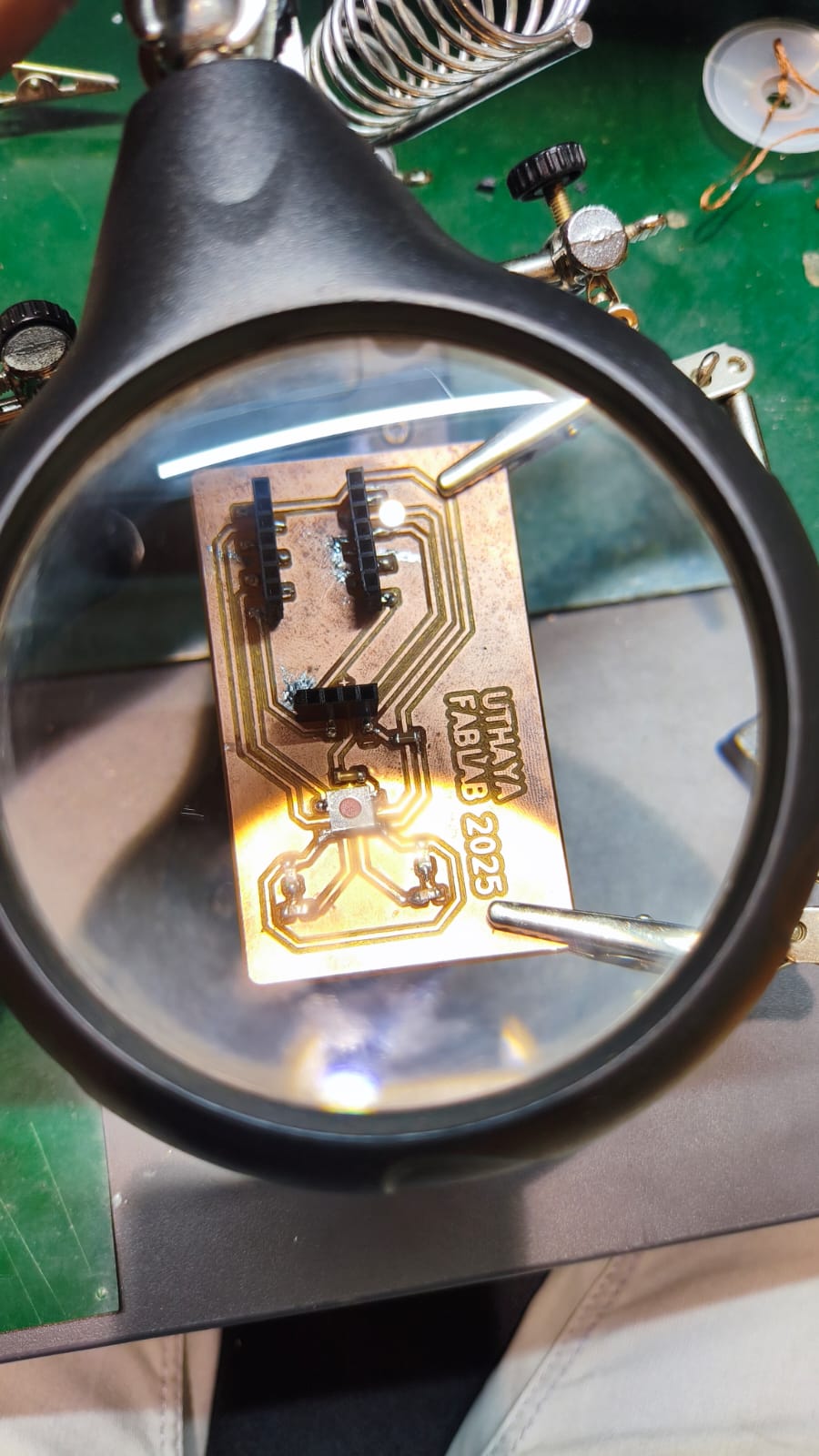
Since my pcb was ready next step is to gather all the components for soldering.
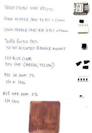
- I followed this diagram to solder the components
- These are the soldering components available in our trichy fablab.
- I started off by soldering the microcontroller onto the pcb at two corners so that its position would be fixed for easy soldering.
- Here's the board after 95% of soldering process (LEDs are left).
- Here is the finished product following the entire soldering procedure.
Programming & Testing :
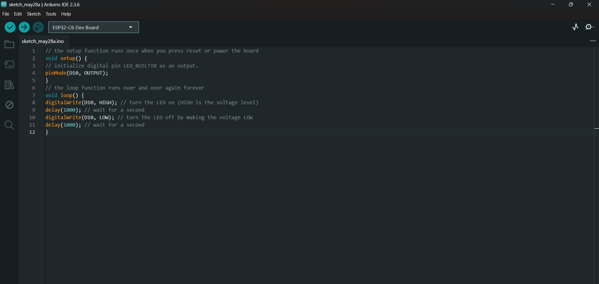
I Uploaded the Code to my Arduino
So now we have to program and test the board to make sure it works properly.
- Open the Arduino IDE.
- Copy the code below and paste it into a new sketch for Blink the led.
      // the setup function runs once when you press reset or power the board

                void setup() {

                  // initialize digital pin LED_BUILTIN as an output.

                  pinMode(D10, OUTPUT);

                }


                // the loop function runs over and over again forever

                void loop() {

                  digitalWrite(D10, HIGH);  // turn the LED on (HIGH is the voltage level)

                  delay(1000);                      // wait for a second

                  digitalWrite(D10, LOW);   // turn the LED off by making the voltage LOW

                  delay(1000);                      // wait for a second

                }
- I Connected my board to computer.
- Then i Select the correct board and port from the Tools menu.
- Finaly i Click the Upload button (right arrow) to upload the code to board.