Electronics
Back
FABLAB 2025
Electronic design
I start my final project PCB design with KiCAD
KICAD
KiCad is a free, open-source software suite for Electronic Design Automation (EDA). It allows users to design schematics and convert them into PCB layouts. KiCad supports multi-layer boards, custom footprints, and 3D visualization of PCB designs.
I import the Fablab library already in the Kicad, I recommend to you to dowload and upload it into your kicad software.
At first I load the microcontroller XIAO ESP32S3 board, then take the pin connectors according to my use.
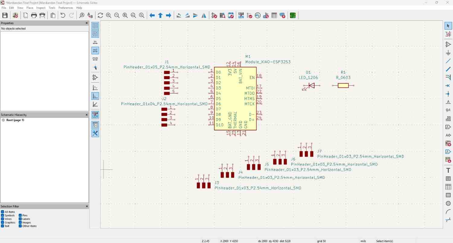
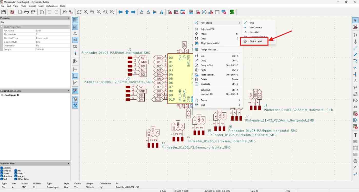
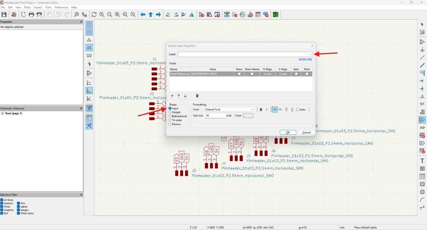
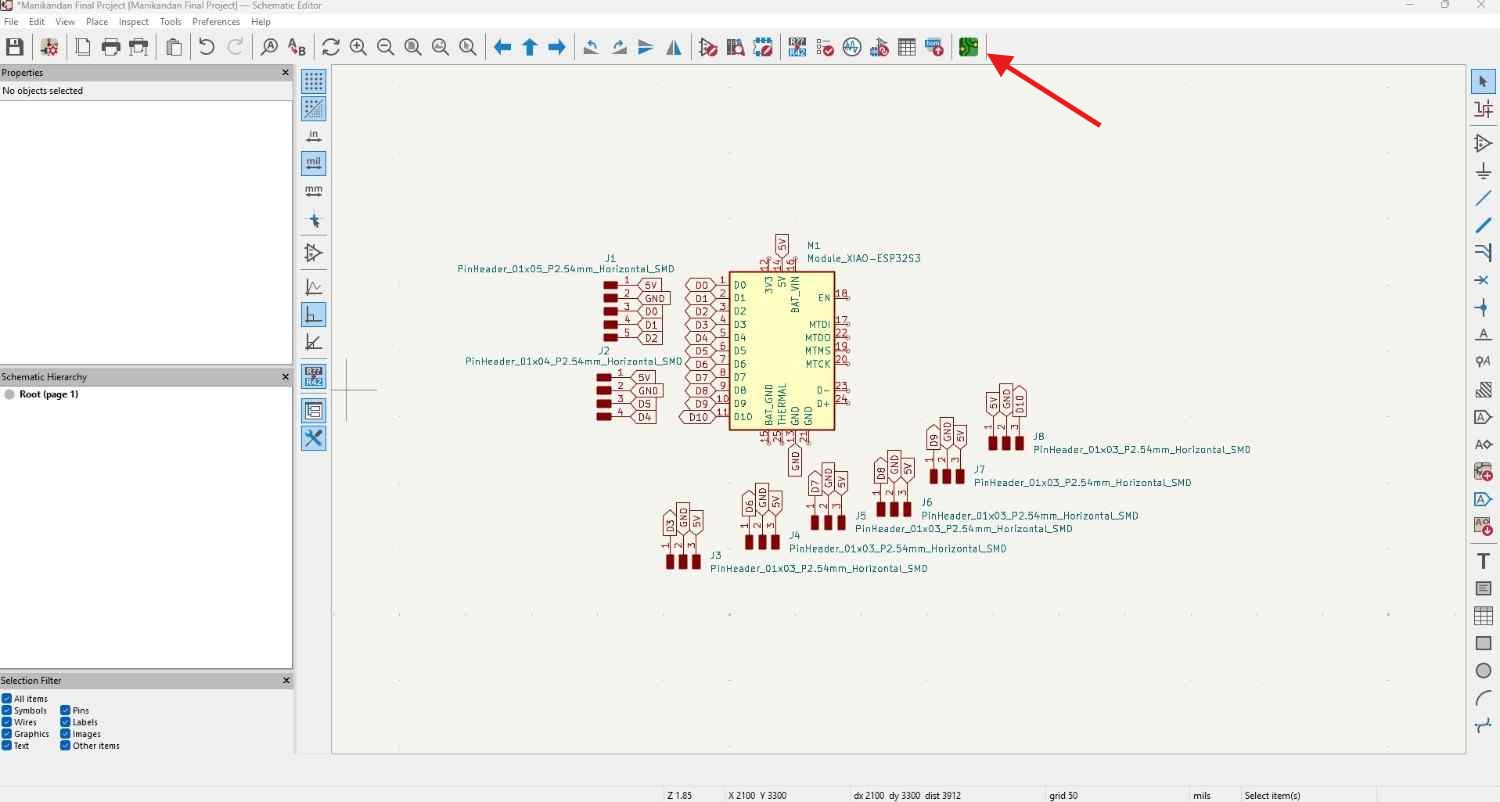
Instead of connecting wiring I set it all by lable, it is very useful whenever you want to change the connections after checking your footprint we can easily change by using those.
After setting all the connection of my board I go into the PCB editor
We should update our current model whenever we did some changes in the schematic editor.
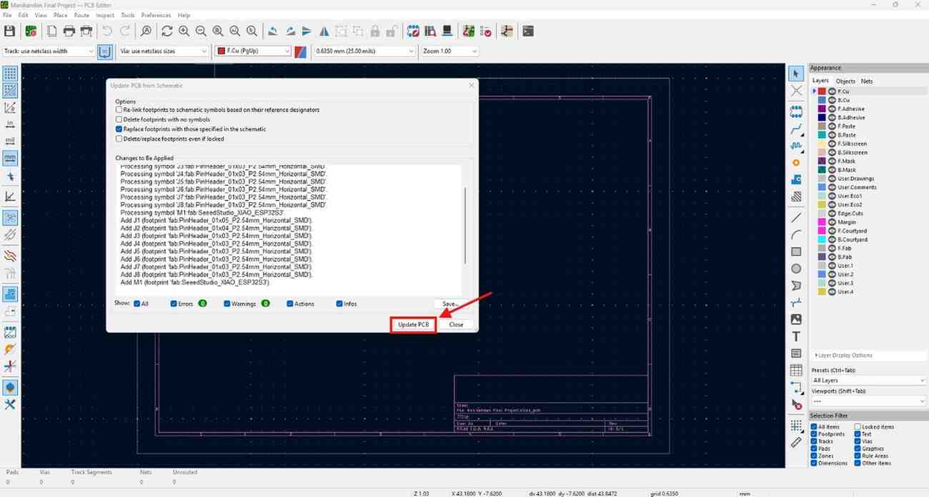
After give the update our footprint design will appear like this, then we need to rearrange our components where we want.
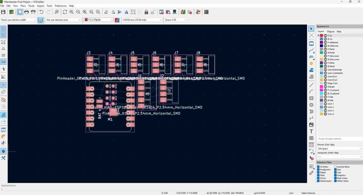
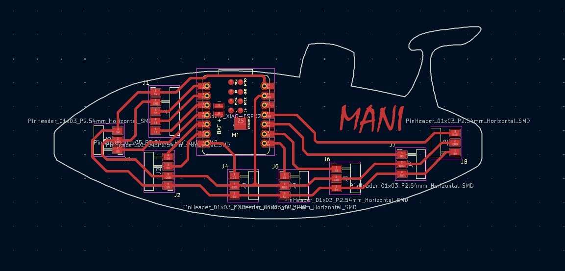
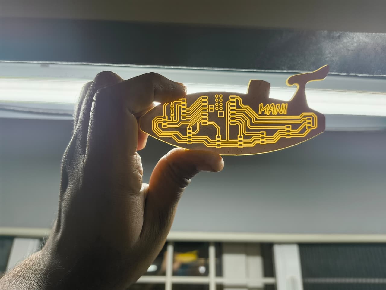
For the edge lines I planned to do different, instead of giving the box or round I aimed to cut the PCB board like my drone shape.
So I open the Fusion 360 and took my drone as reference and draw the outer line for the edge cut.
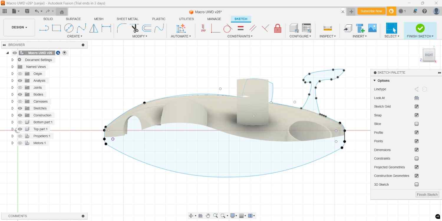
Then I extrude it by using the extrude command because the design is not the proper design so we should be contraint it before export it.
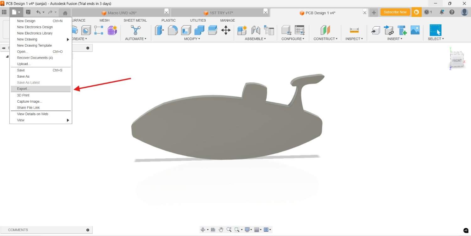
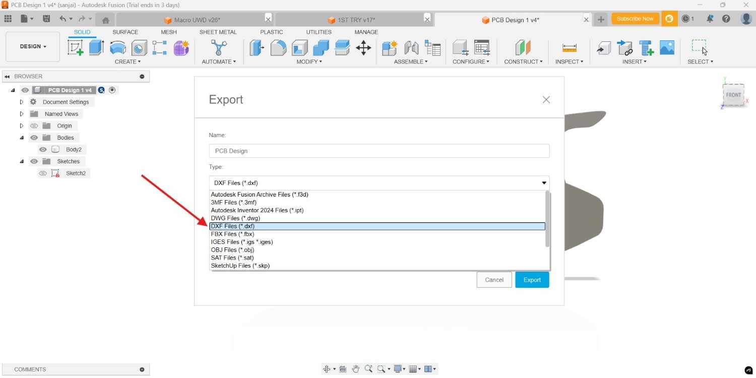
I export it into DXF file to import the Kicad. Kicad will support the DXF format so there is no issue
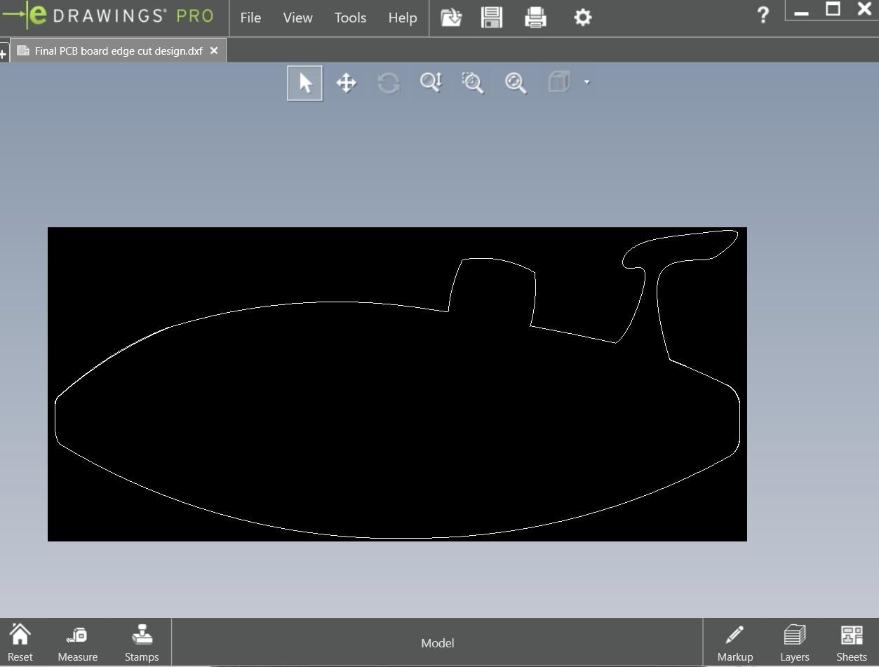
I am also checking that whether is it came without broken by using the e drawings, its just the dxf viewer
I import it into the Kicad and rearrange the components positions within only inside the edge cut, then by using the trace I connected teh componets
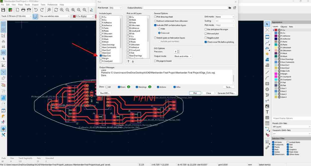
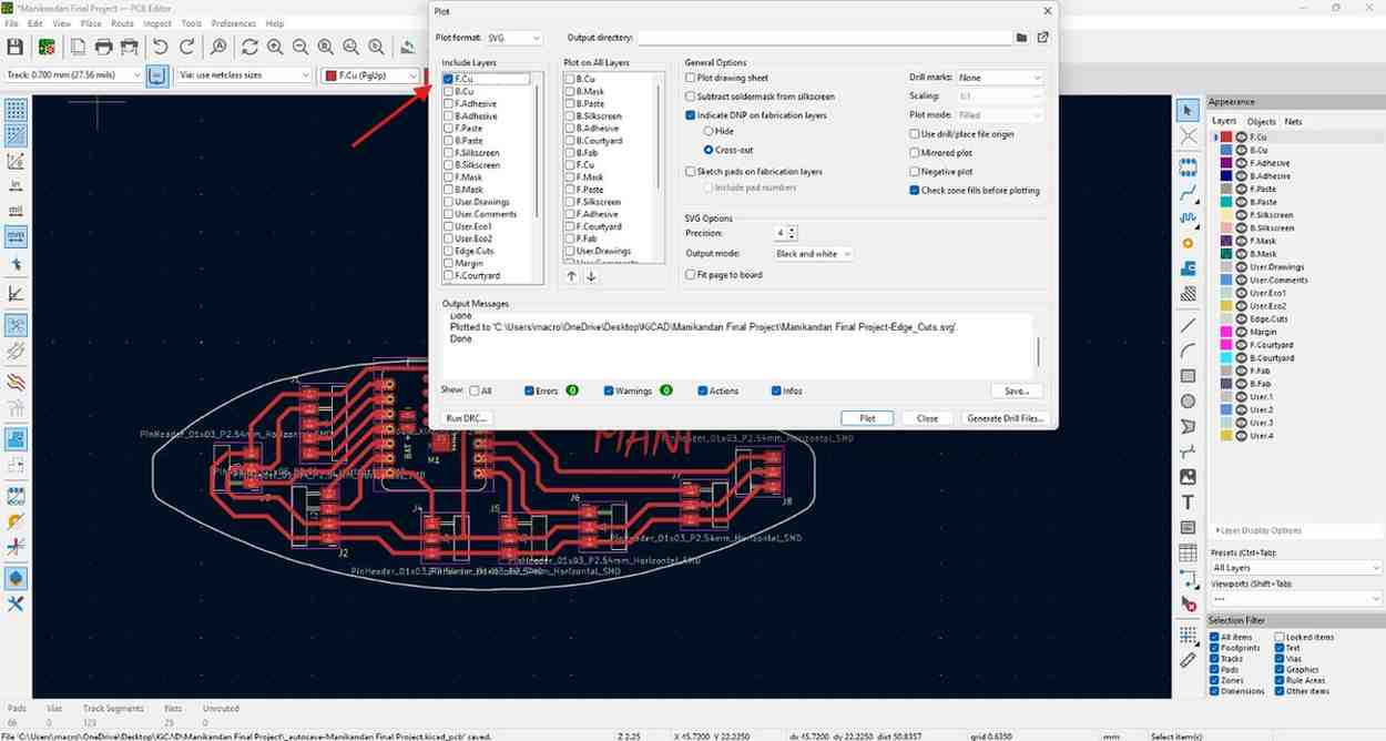
To export it I used the SVG export option in Kicad
Electronic Production
MODS
MODs (Machines, Objects, and Devices) is an open-source software tool developed by MIT's Center for Bits and Atoms. It provides a modular, browser-based interface for controlling digital fabrication machines like laser cutters, vinyl cutters, and CNC mills. Users can create custom toolpaths from various file formats (e.g., SVG, PNG, STL). It allows real-time editing of fabrication parameters using a node-based flow system. MODs is lightweight and runs locally in a browser, offering flexibility for custom workflows. It's especially popular in Fab Labs and educational environments.
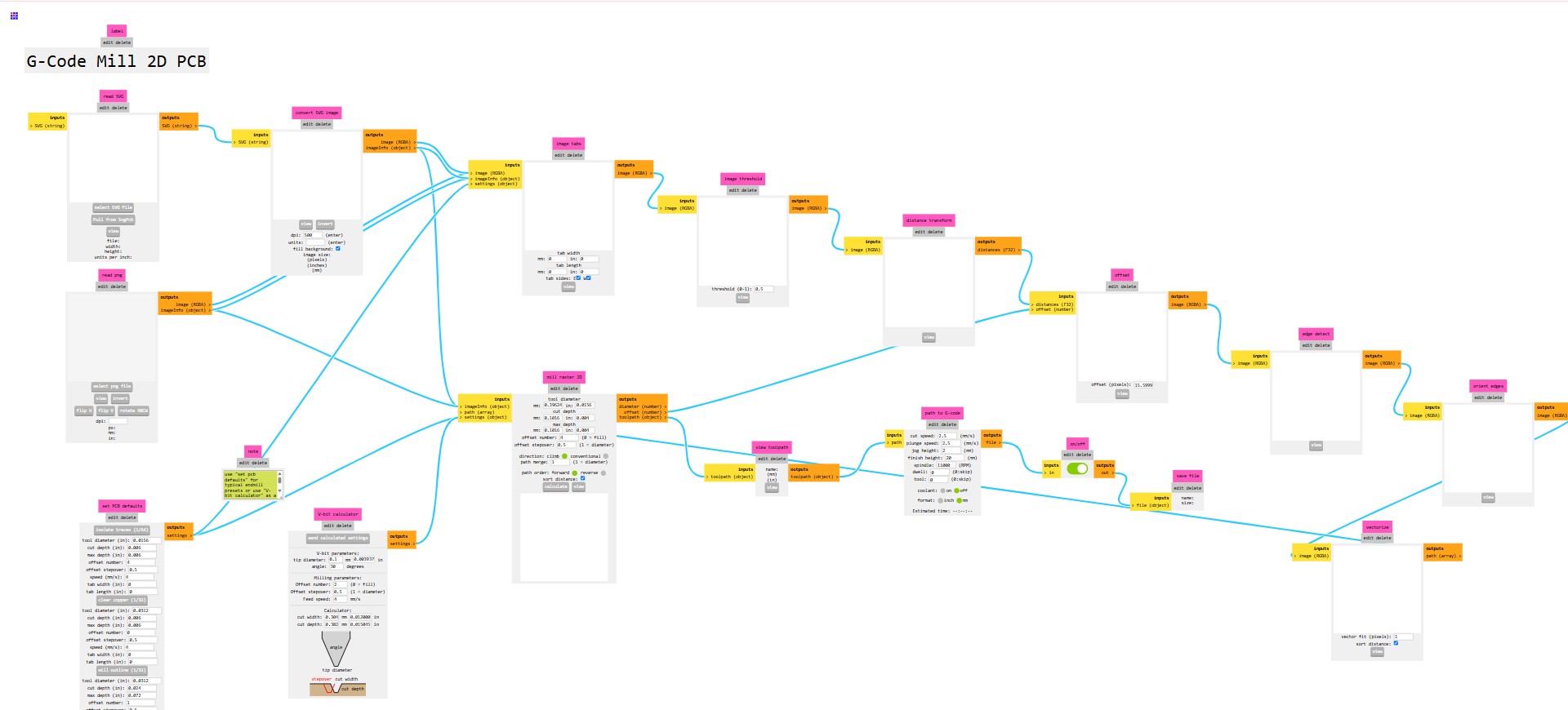
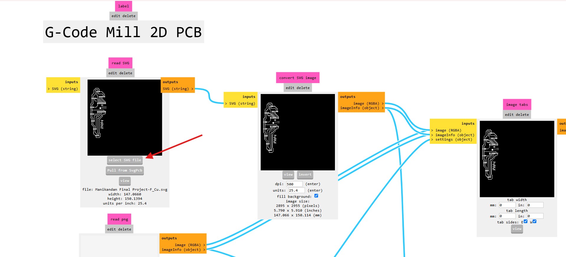
For my PCB milling I need a tool path so I use the MODS to generate the gcode
Right-click to open a program and go to the G-code 2D PCB Milling, after enter into that load files PNG/SVG for processing (Right click>Program>open program>G-code - mill 2D PCB)
After open the Gcode pcb mill we should load our SVG file of our pcb design
Then I set the parameters according to my machine capability, every machine has good capability with some certain parameters
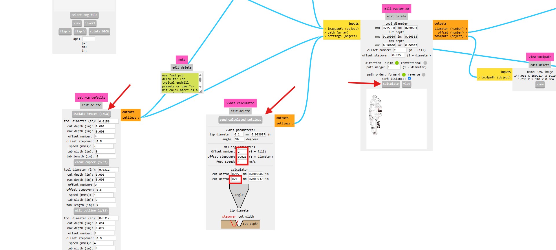
After done those all I give the calculate, so it will download the gcode of our design
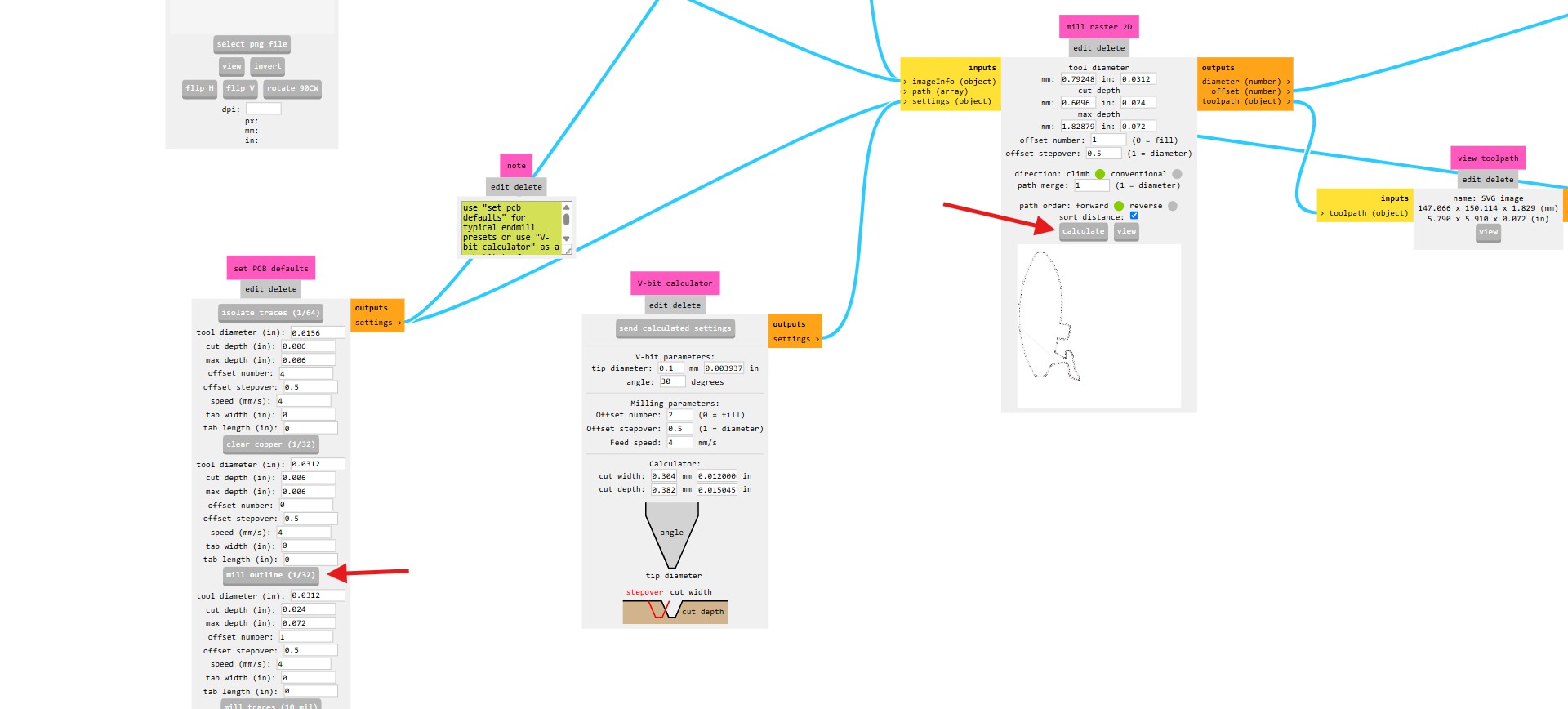
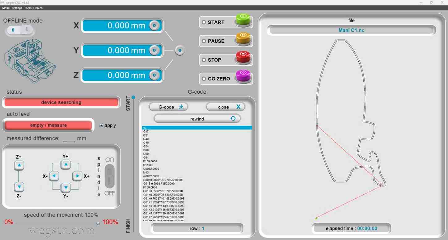
Further I did the edge cut as well to take out the gcode
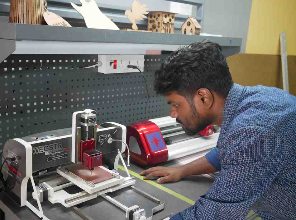
Wegstr
Wegstr provides free CNC Controlling Software for operating its milling machines on Windows, macOS, and Linux. It enables basic operations like PCB milling and engraving. For designing toolpaths, Wegstr recommends Cut2D Desktop.
For the milling operation I used the Wegstr software to control our Wegstr machine. I import the gcode in the software
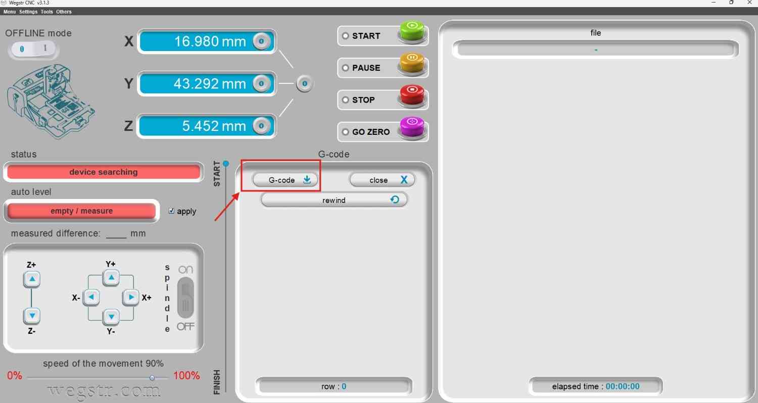
I check the gcode whether it is properly came or not once, Iset the position of the spindle where from I want to milling.
I also check once the edge cut before milling for the proper positioning
Milling Process
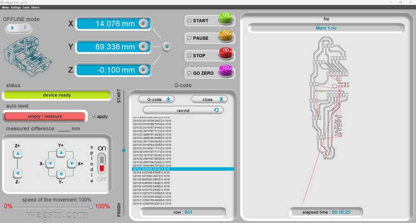
I start the milling process by Wegstr software,
I closely check the milling process to confirm the trace width came better as expected
After the milling I changed the cutting tool to the spindle without changing the X & Y axis, only changed the Z axis. Then set again zero to the edge cut.
The cutting process done wihtout any damage
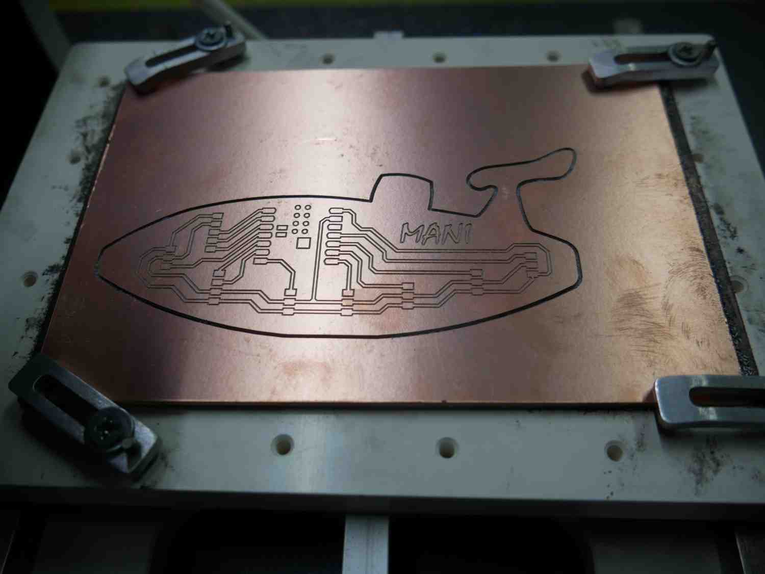
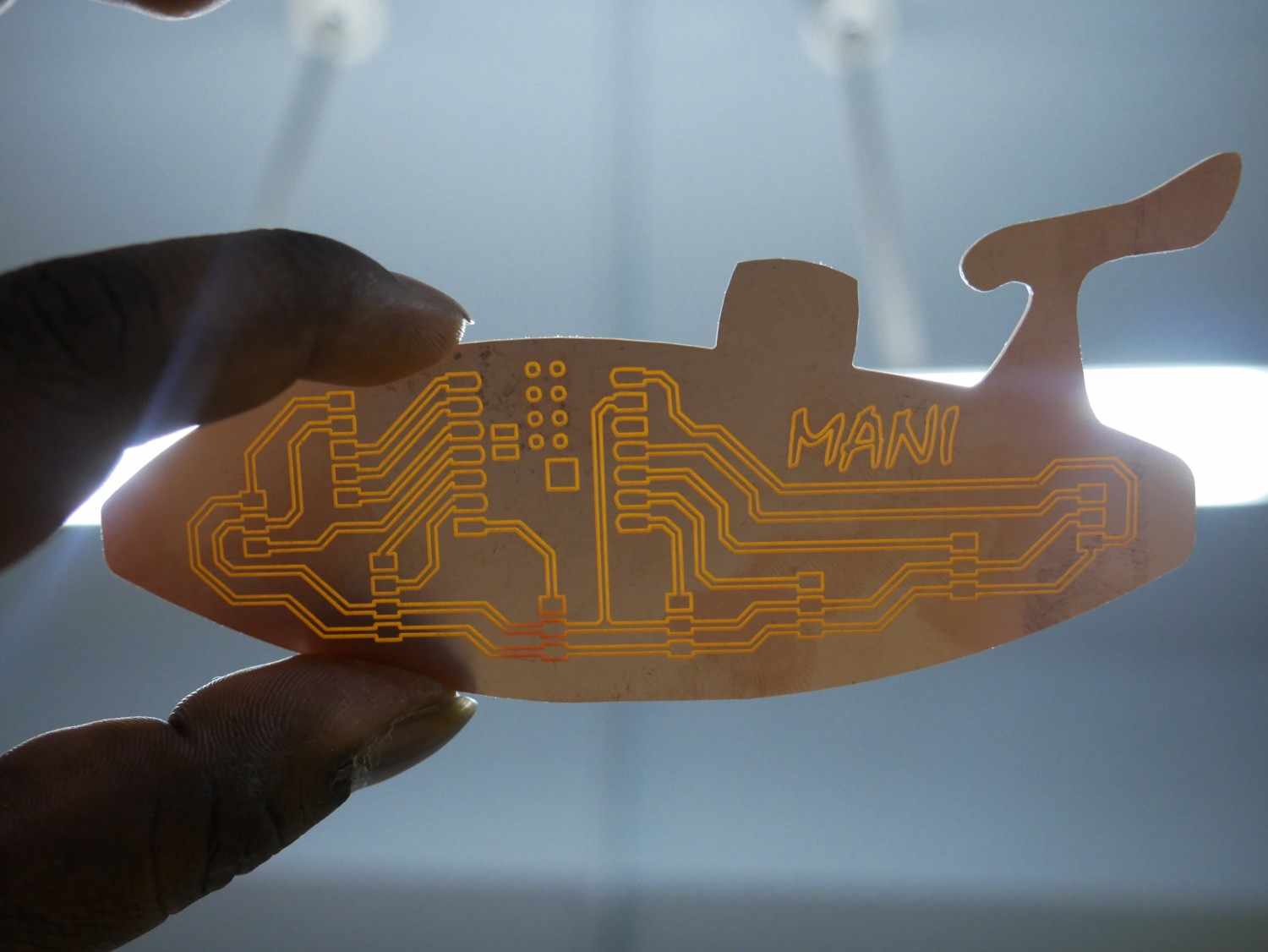
Milling also came good as I expected…
Soldering
I check the PCB board continuity test by using the Multimeter, after setting the continuity I check wiht the probe itself.
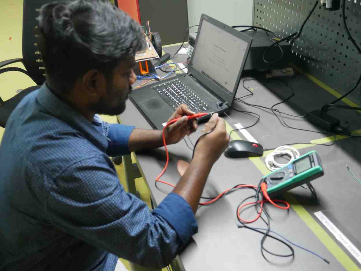
Then I place the probe at differnt places to confirm the milling came without any damage
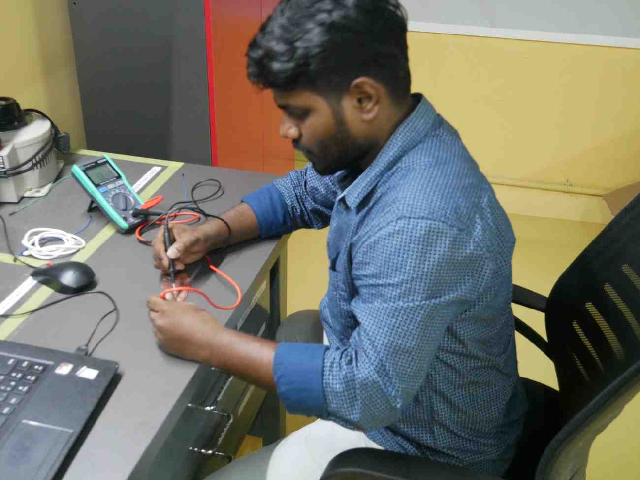
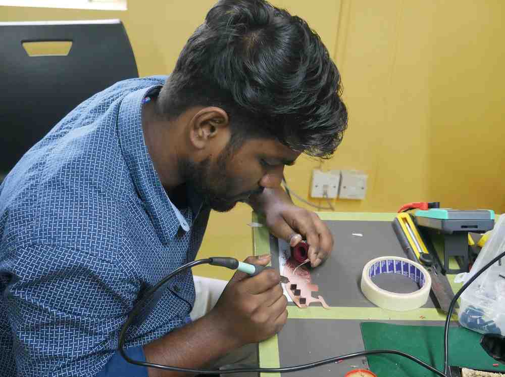
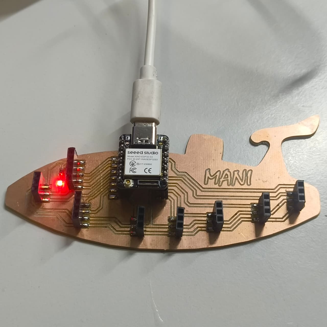
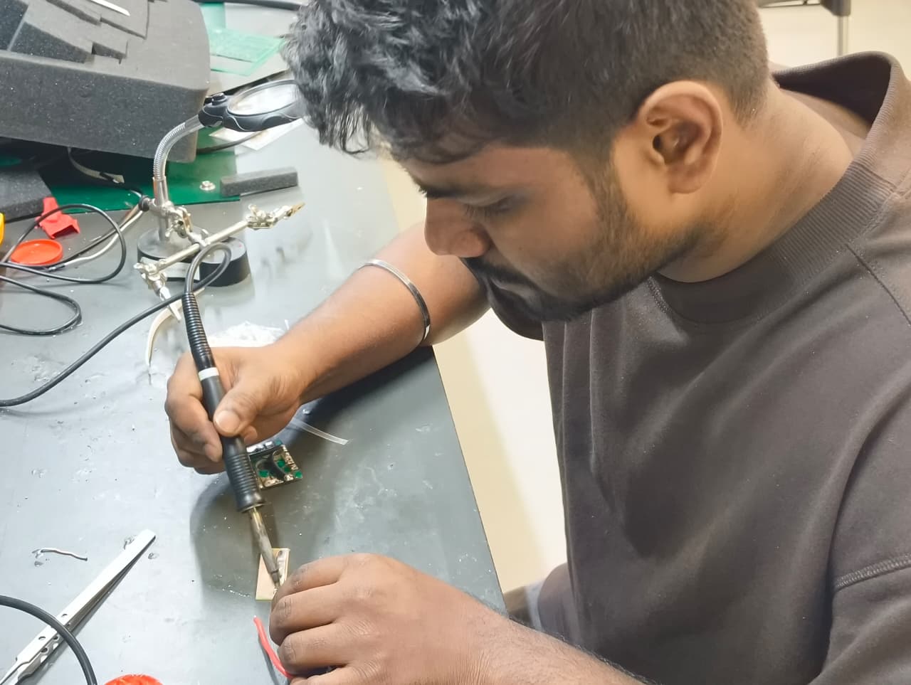
After confirming everything I took the board to soldering the pin connectors and the microcontroller, I carefully soldering those
FABLAB 2025
PCB Re-Fabrication and Electronics Preparation
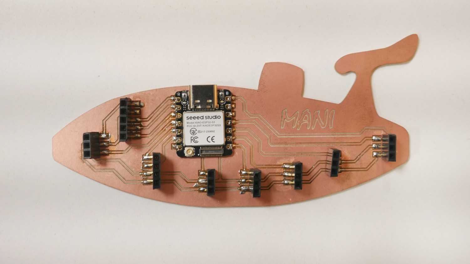
During the assembly phase of the underwater drone, I identified that the previously fabricated control board had been damaged and could not be reliably used for further integration.
To ensure the successful completion of the prototype, I decided to redesign and fabricate the PCB once again.
While redesigning the board, I also took the opportunity to incorporate a simple visual indicator circuit consisting of an LED and a current-limiting resistor.
This addition would help verify power availability and basic board functionality during testing.
PCB Redesign
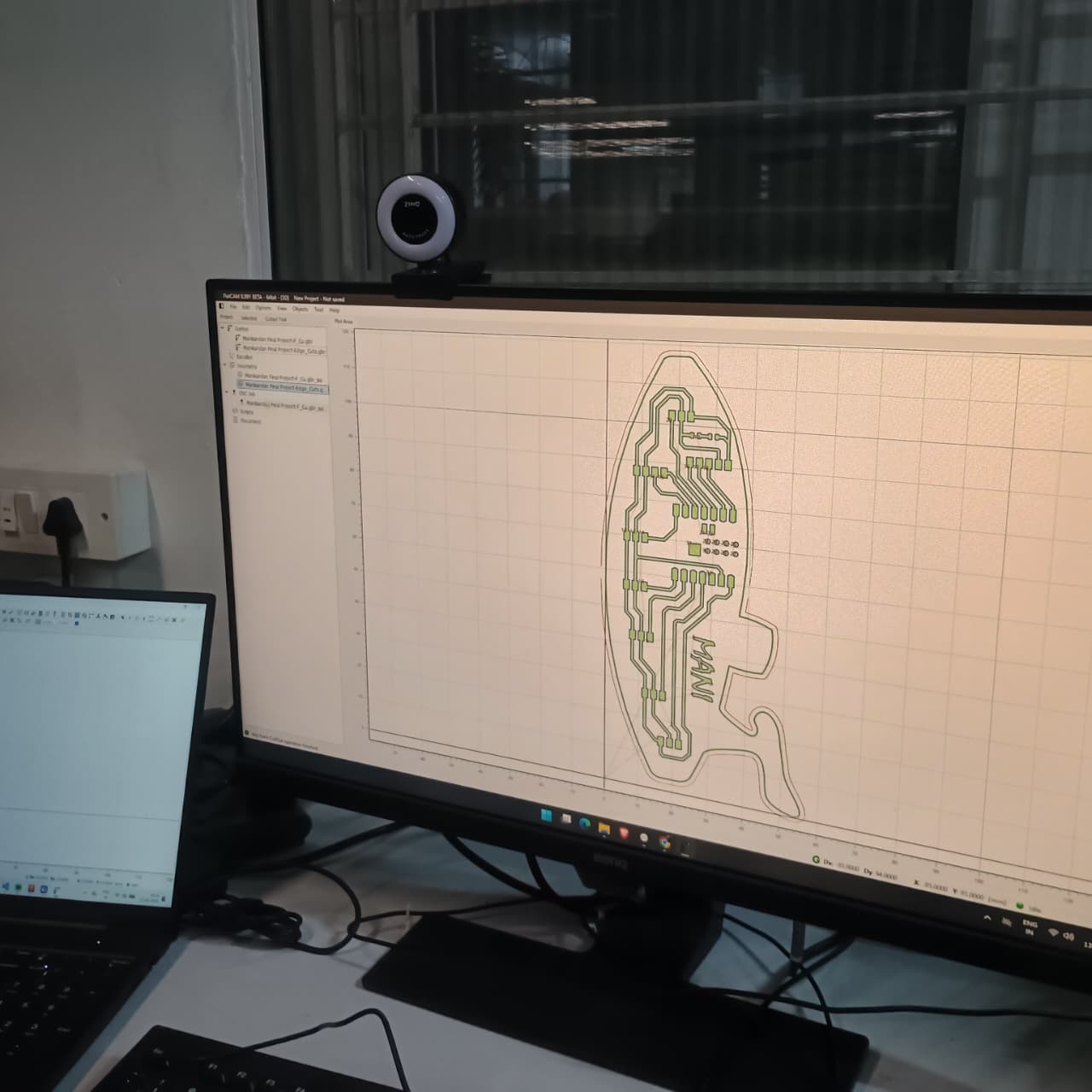
The original PCB featured a fish-shaped outline inspired by the underwater nature of the project.
The schematic was updated to include the LED and resistor components. In addition, several PCB traces were adjusted and rerouted to improve component placement and ensure that all connections fit properly within the custom board outline.
After completing the schematic and PCB layout modifications, the design rule checks were verified and the required manufacturing files were generated.
Once the PCB layout was finalized, Gerber files were exported from the design software. These files were then processed to generate the machining toolpaths required for PCB milling. The corresponding NC files were also created for both trace milling and board cutting operations.
PCB Fabrication
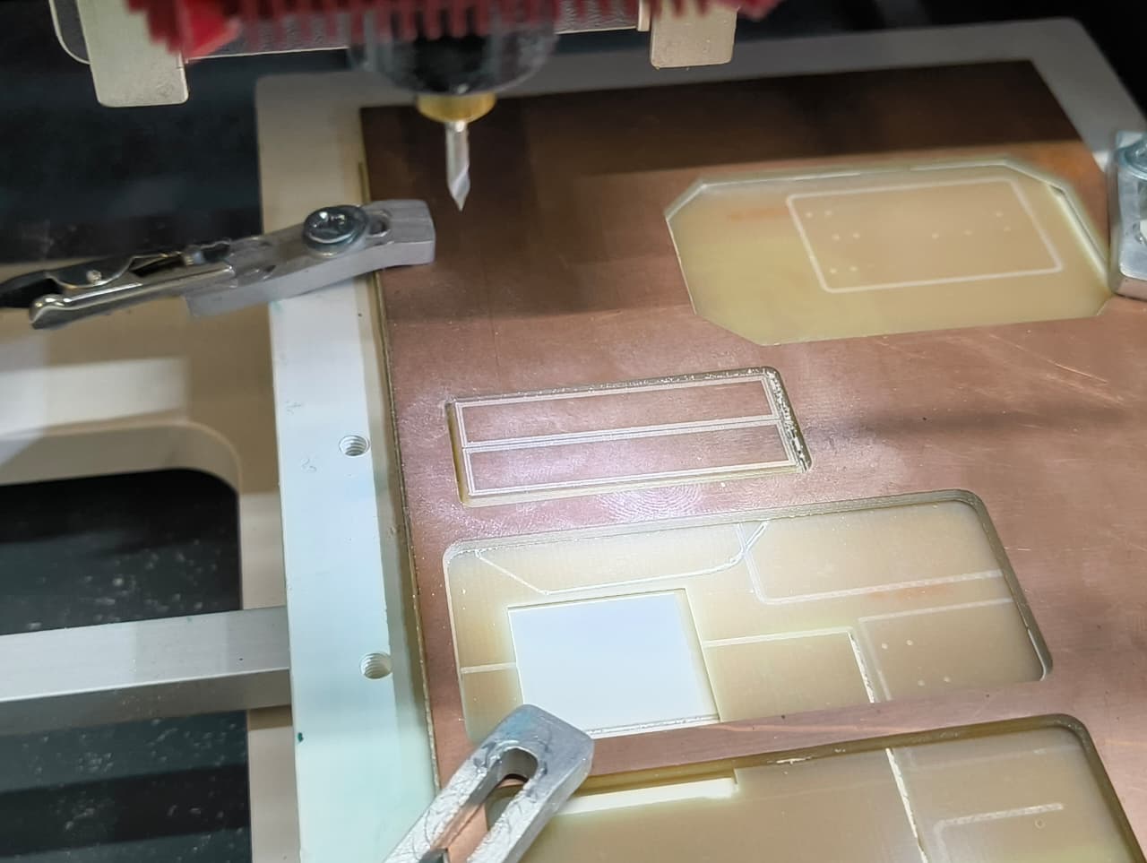
The updated PCB was fabricated using the PCB milling machine following the same workflow that had been successfully used in previous work. The machine was configured with the required milling parameters, and the traces and board outline were machined directly onto the copper-clad material.
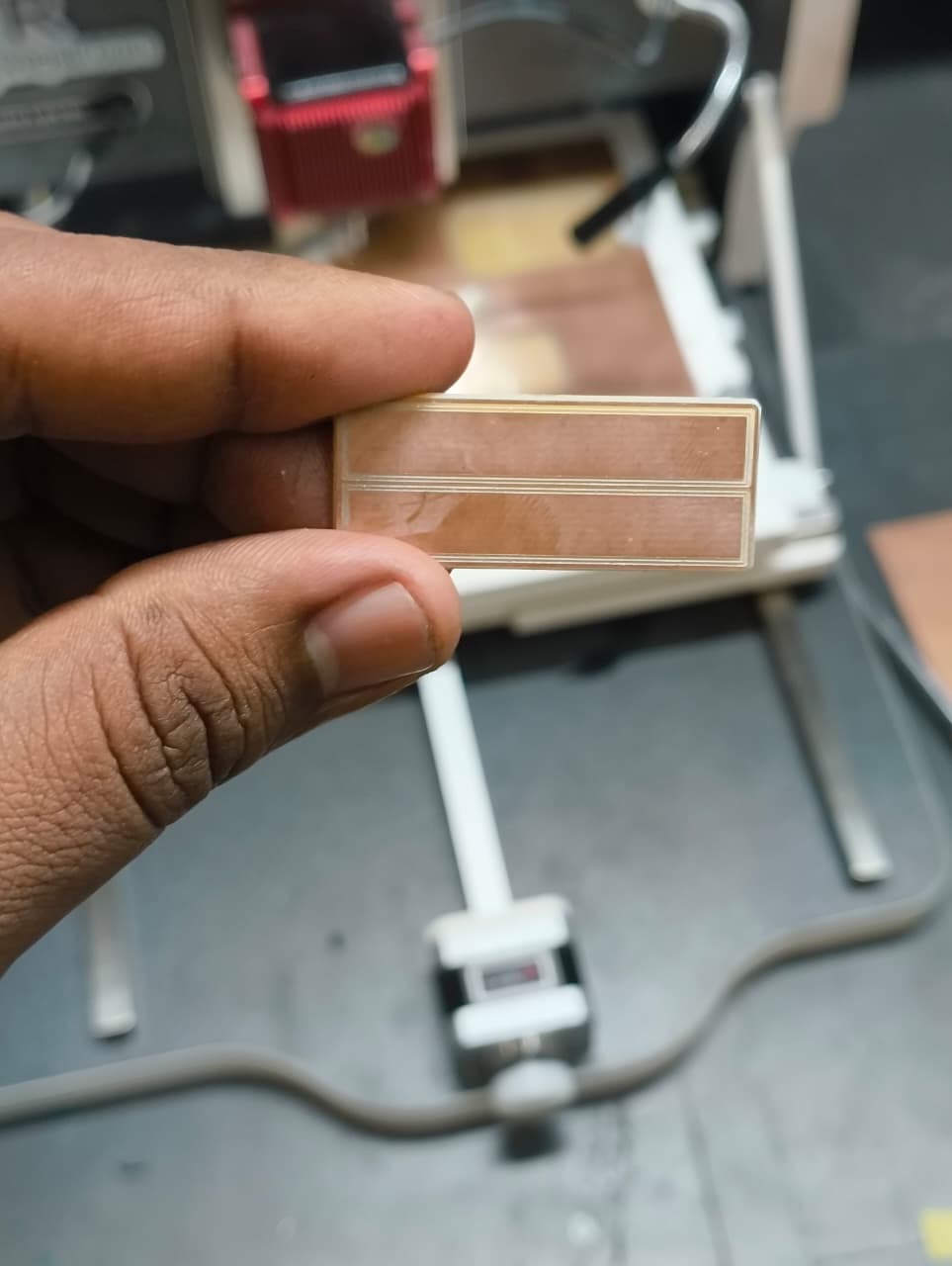
After completing the milling process, the PCB was cleaned and inspected to verify trace quality and dimensional accuracy. The board was then separated from the stock material and prepared for component assembly.
Following fabrication, the required electronic components were soldered onto the PCB. Pin headers were installed to accommodate the microcontroller, and motor connectors were added to support future integration with the brushless motor control system.
The LED and resistor were also soldered onto the board to provide a simple status indication feature. Care was taken to ensure reliable solder joints and proper component alignment throughout the assembly process.
Power Distribution Board
To improve the electrical connections for the Electronic Speed Controllers (ESCs), I decided to create an additional PCB dedicated to power distribution.
The purpose of this board was to provide a more organized and reliable method for connecting the positive and negative power lines.
Using KiCad, I designed a simple PCB consisting of large copper areas arranged in a box-like structure to accommodate multiple power connections.
After completing the layout, the Gerber files were exported, NC files were generated, and the board was fabricated using the PCB milling machine.
Once the fabrication process was completed, the power wires were soldered onto the board according to their respective positive and negative terminals.
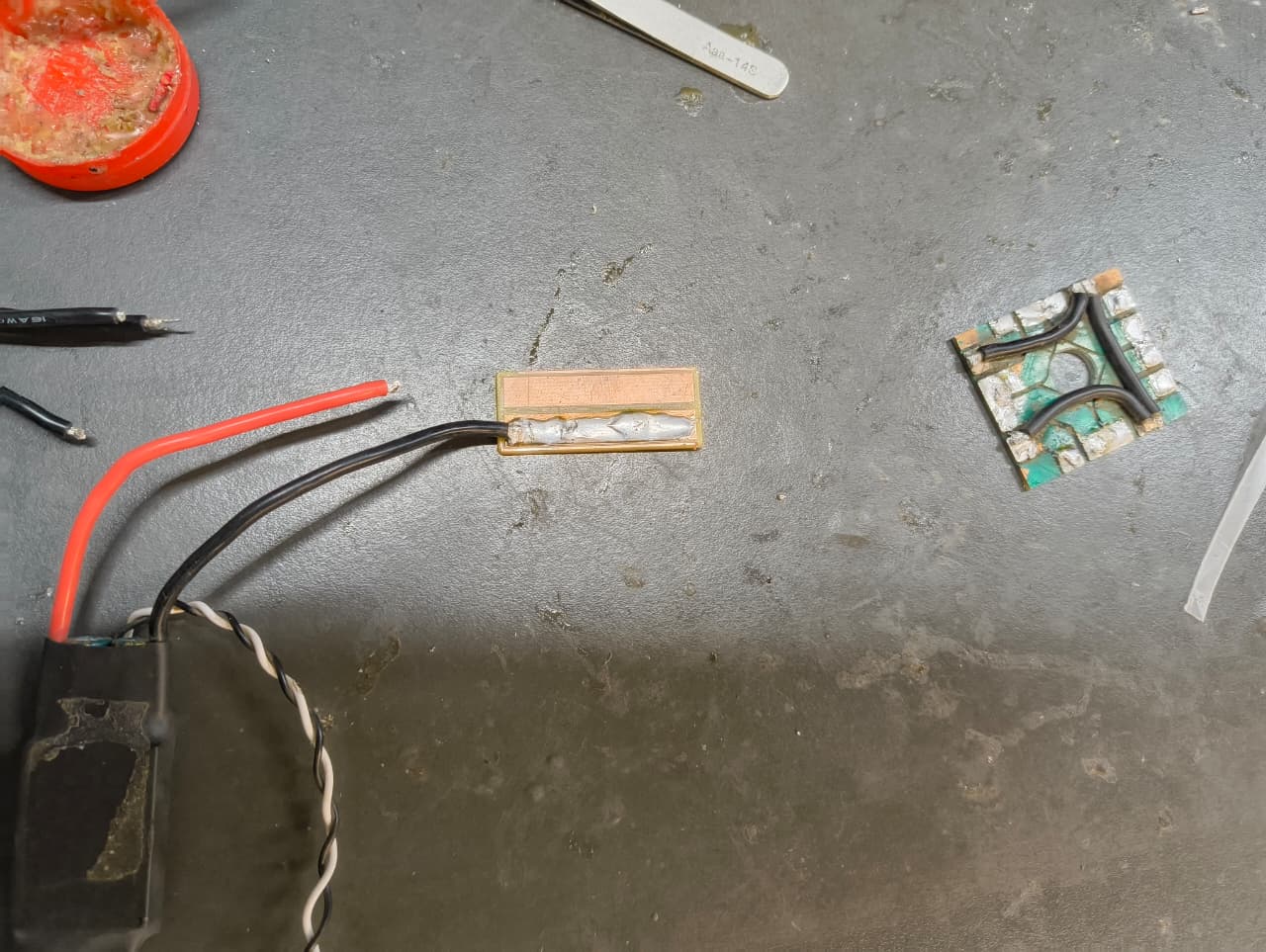
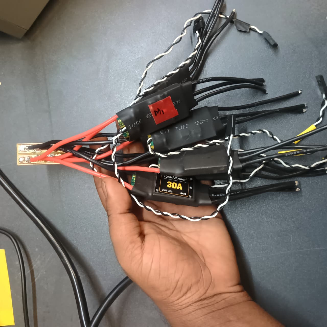
This created a cleaner and more secure power distribution system for the ESC connections and simplified the overall wiring arrangement inside the drone.