KiCAD (PCB + FootPrint)
Summary
After completing the schematic design, I moved on to designing the PCB layout and selecting the correct footprints for my components. Using KiCad’s PCB Editor, I transferred my schematic, arranged the components, and started routing the connections. This process ensured that the PCB was optimized for manufacturing and functionality.
Work Process Detail
1. Transferring Schematic to PCB Editor
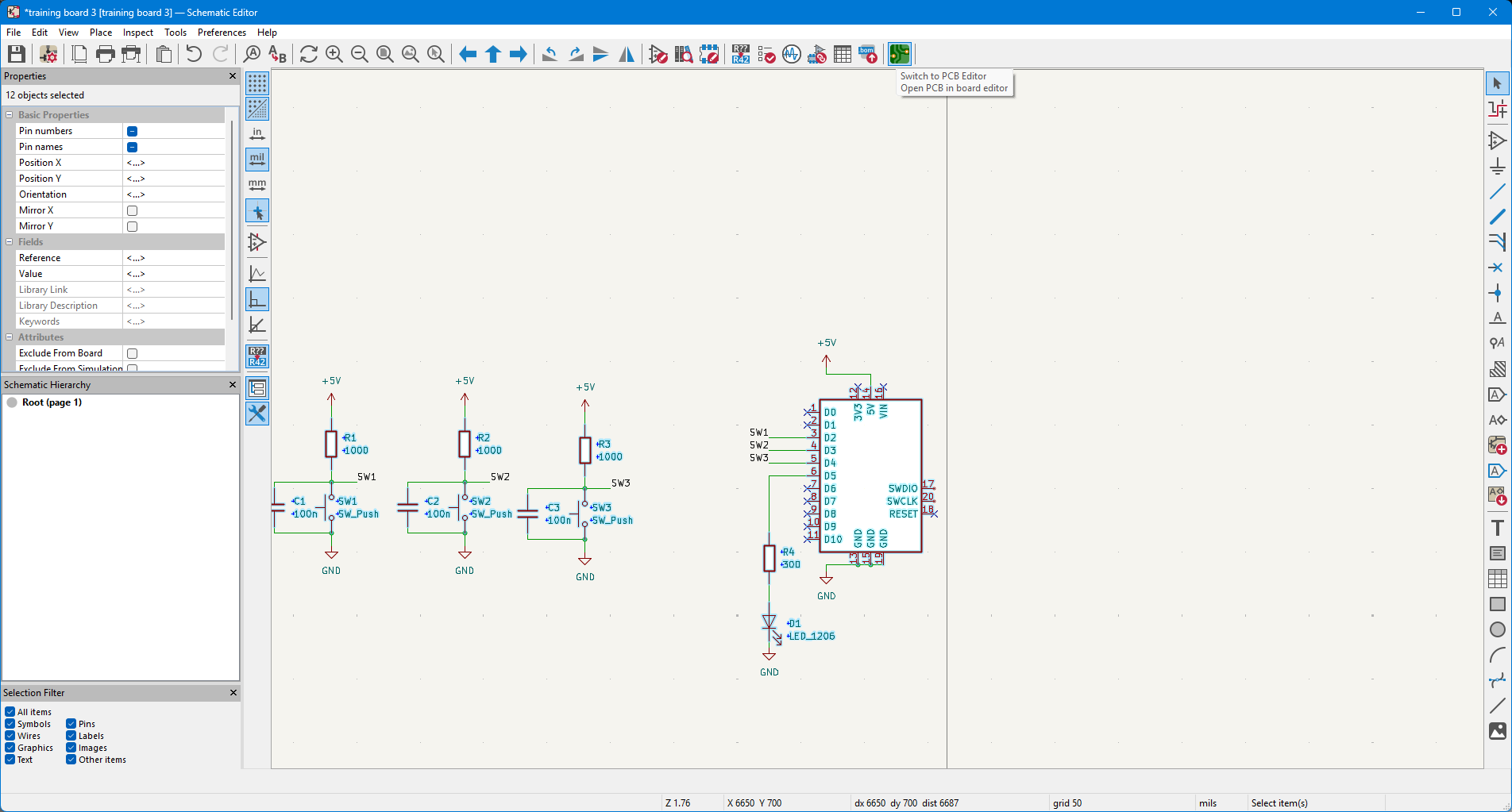
- From the Schematic Editor, I selected the option to switch to the PCB Editor.
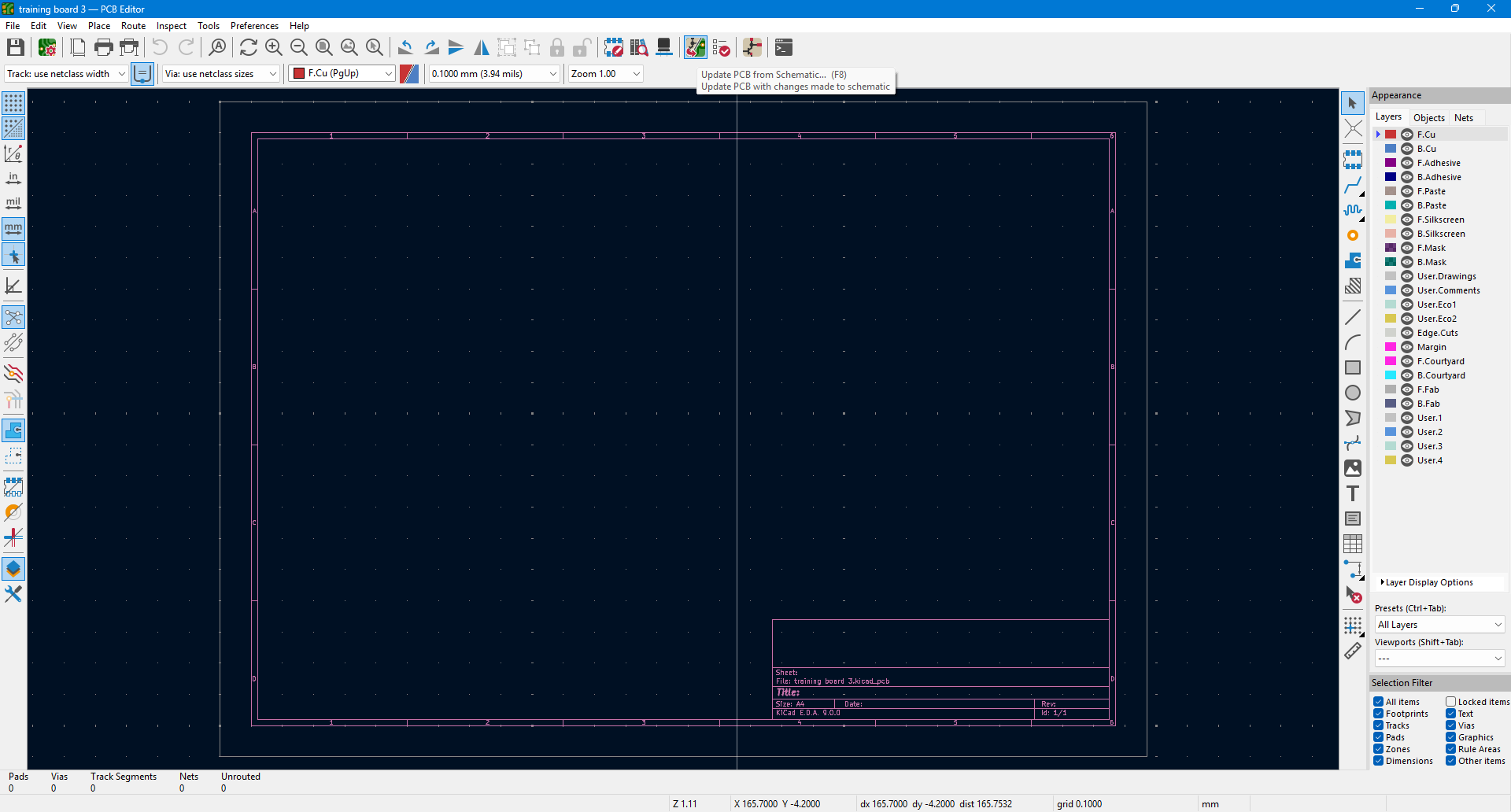
- Once in the PCB Editor, I clicked "Update PCB from Schematic", which imported the footprints of all the components from the schematic.
2. Checking for Errors and Warnings
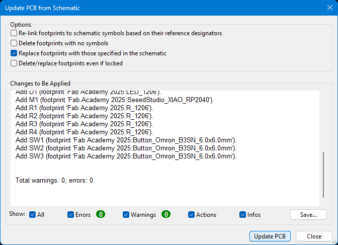
- After updating the PCB, I verified that there were no errors or warnings in the component placement.
- Ensured that all footprints were correctly assigned and visible in the workspace.
3. Placing and Aligning Components
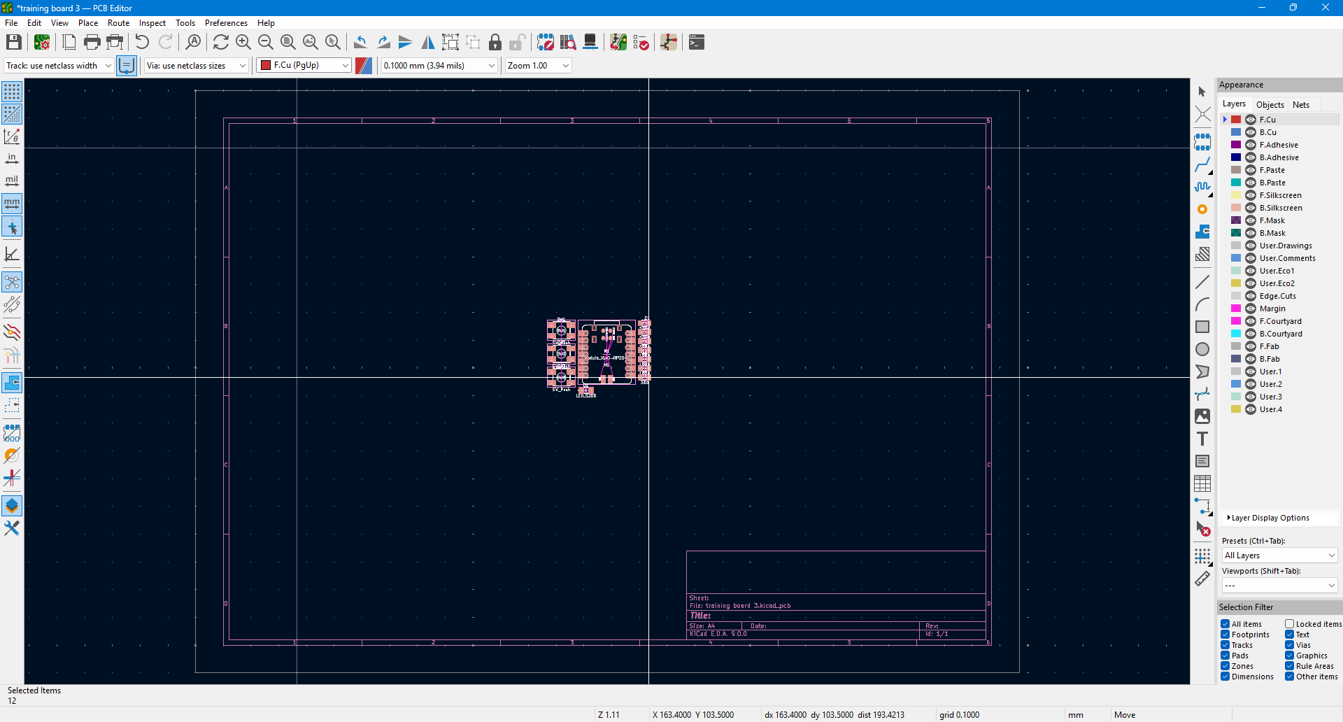
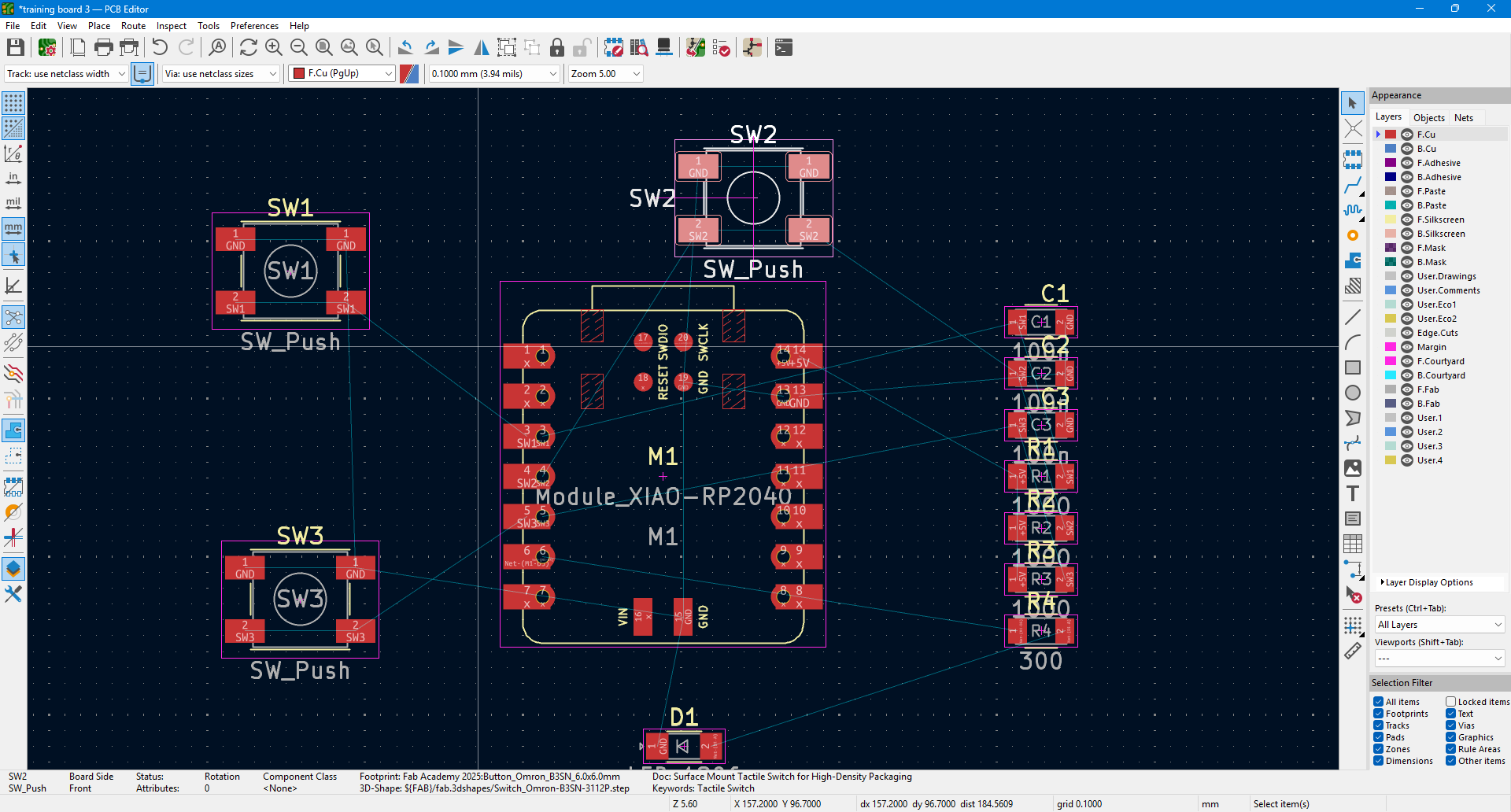
- I began dragging and placing each component in an optimal position based on the PCB layout.
- Ensured proper spacing and alignment to avoid overlapping traces.
- Considered routing efficiency and component accessibility for soldering and debugging.
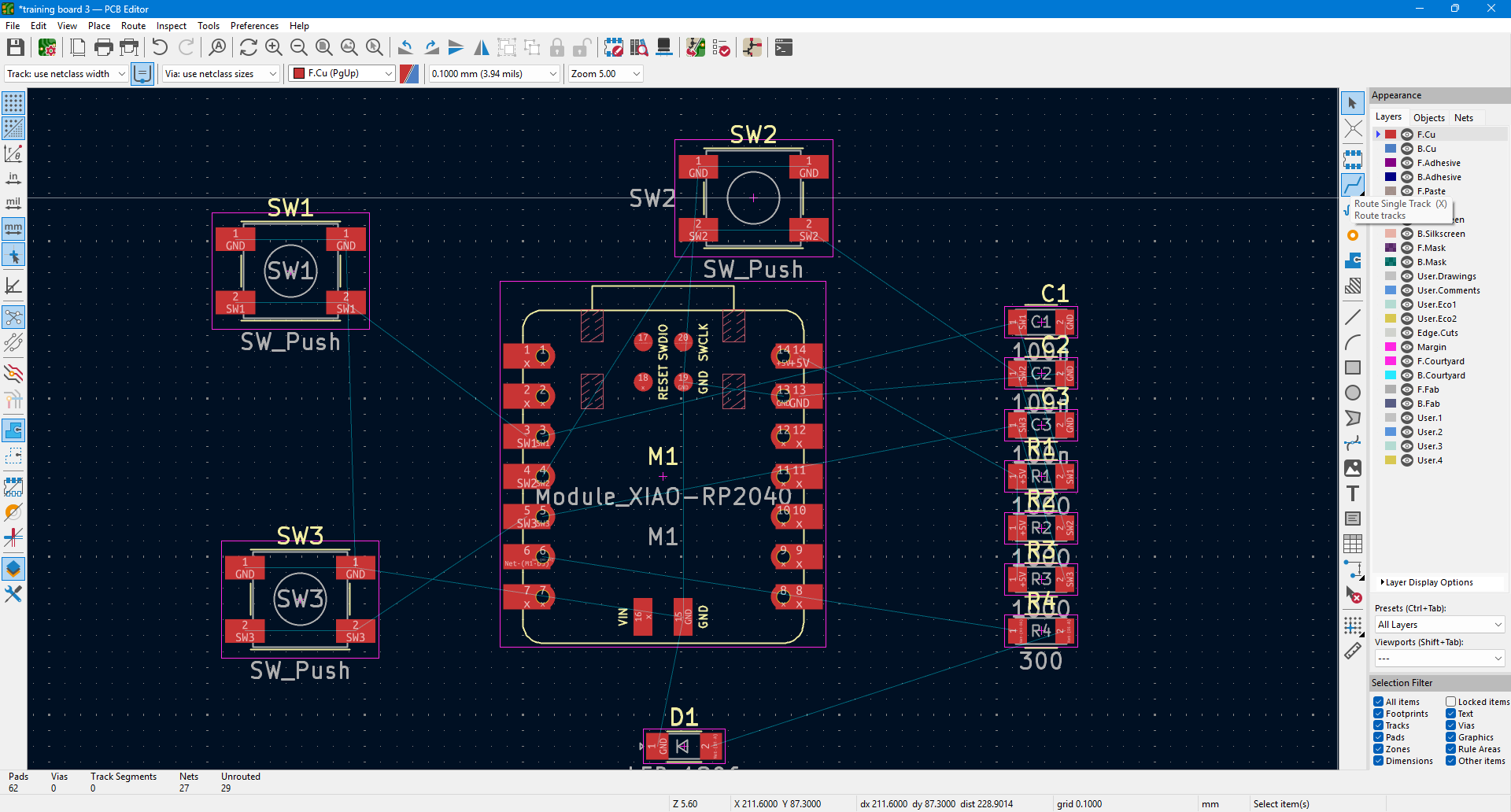
4. Routing the PCB Connections
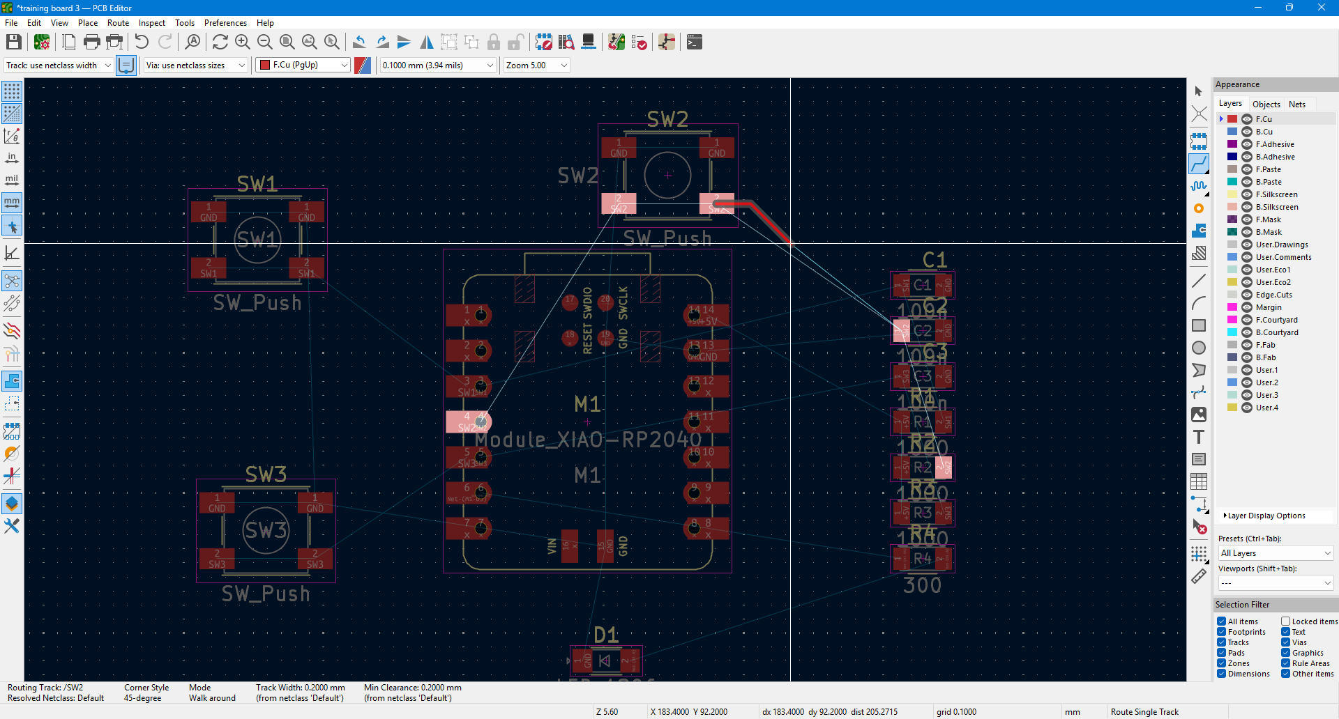
- After placing the components, I started routing traces to connect different parts.
- Ensured clearance between traces, using proper widths for power and signal lines.
- Followed best practices for ground planes and power distribution to minimize noise.
Failure
Learning Outcome
1️⃣ Switched from Schematic Editor to PCB Editor in KiCad.2️⃣ Updated PCB from Schematic, ensuring all footprints were imported correctly.
3️⃣ Checked for errors and warnings before proceeding.
4️⃣ Placed and aligned components based on optimal PCB design requirements.
5️⃣ Routed connections between components, following best practices for PCB layout.
This process helped me understand the workflow from schematic to PCB layout, including footprint selection, component placement, and routing techniques. Moving forward, I plan to finalize routing, add labels, and prepare the PCB for manufacturing.
