KiCAD (Install & Fab Inventory Library )
Summary
This week, I focused on electronic design by creating my own PCB using KiCad. I started by installing KiCad, configuring it with the Fab Academy inventory library, and then designing a PCB based on the RP2040 microcontroller with LEDs. Below is a step-by-step breakdown of the process.
Work Process Detail
1. Installing KiCad
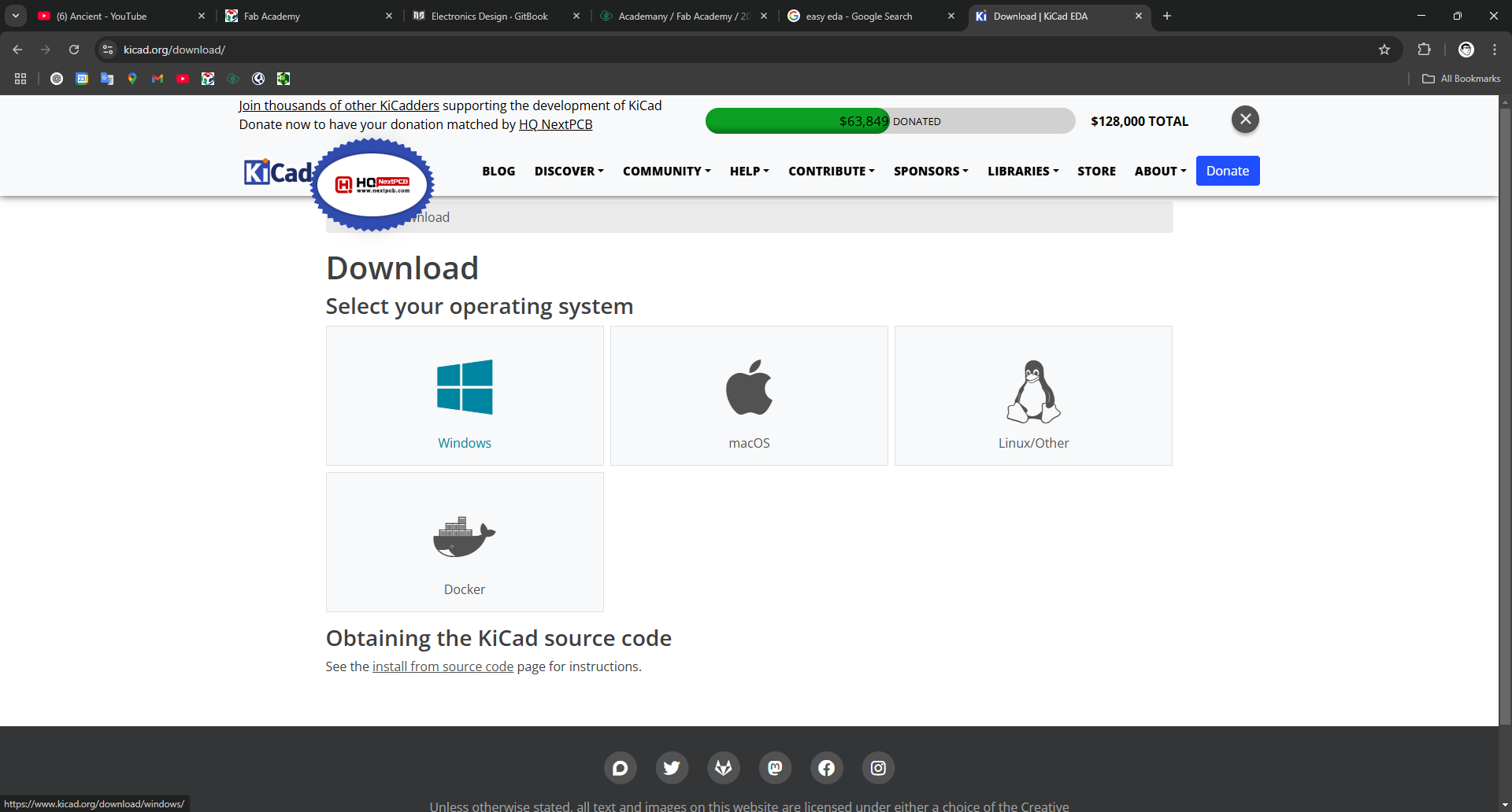
- I visited the official KiCad EDA website and downloaded the Windows version.
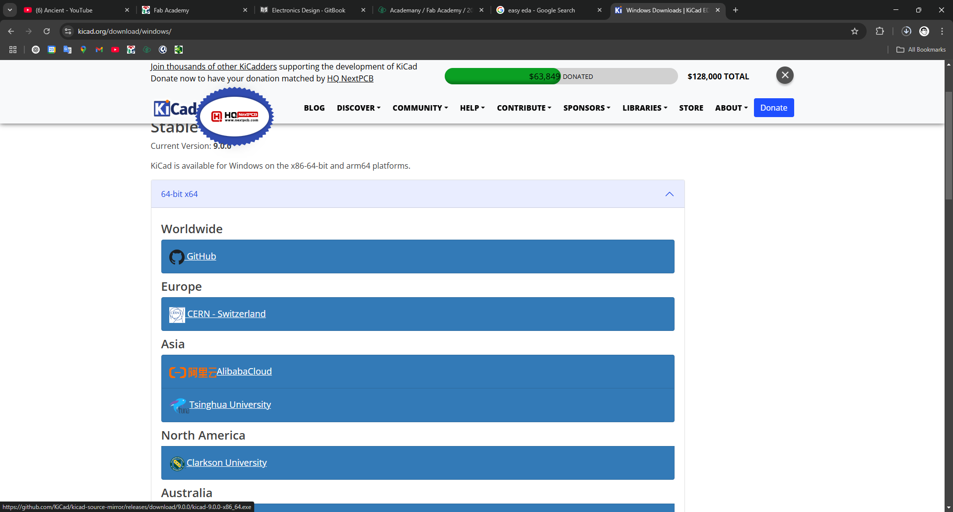
- After downloading, I followed the GitHub installation link to ensure I installed the latest version.
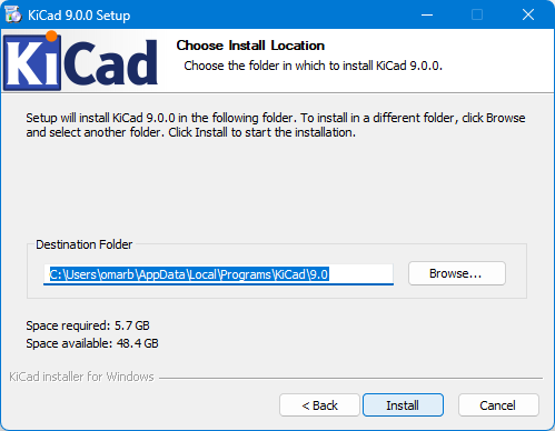
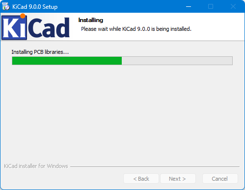
- I proceeded with the installation wizard, clicking Next until the process was complete.
- Once installed, I launched KiCad to confirm that it was working correctly.



2. Adding the Fab Academy Inventory Library
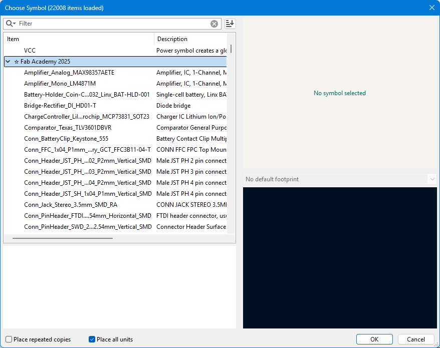
- To make my experience smoother, I added the Fab Academy component library to KiCad.
- I followed the step-by-step instructions from a GitHub repository.
https://gitlab.fabcloud.org/pub/libraries/electronics/kicad
- Clone or download this repository. You may rename the directory to
fab.
- Store it in a safe place such as
~/kicad/librariesorC:/kicad/libraries.
- Run KiCad or open a KiCad
.profile.
- Go to "Preferences / Manage Symbol Libraries" and add
fab.kicad_symas symbol library.
- Go to "Preferences / Manage Footprint Libraries" and add
fab.prettyas footprint library.
- Go to "Preferences / Configure Paths" and add new environment variable "FAB" that points to location of the fab library on your drive, e.g.
~/kicad/libraries/fab. This is needed for the 3D models to load correctly.
- Clone or download this repository. You may rename the directory to
- I imported the schematic symbols and footprint libraries to ensure that all necessary components were available for PCB design.
- After installation, I verified that the library loaded correctly inside KiCad.
3. Creating the PCB Design
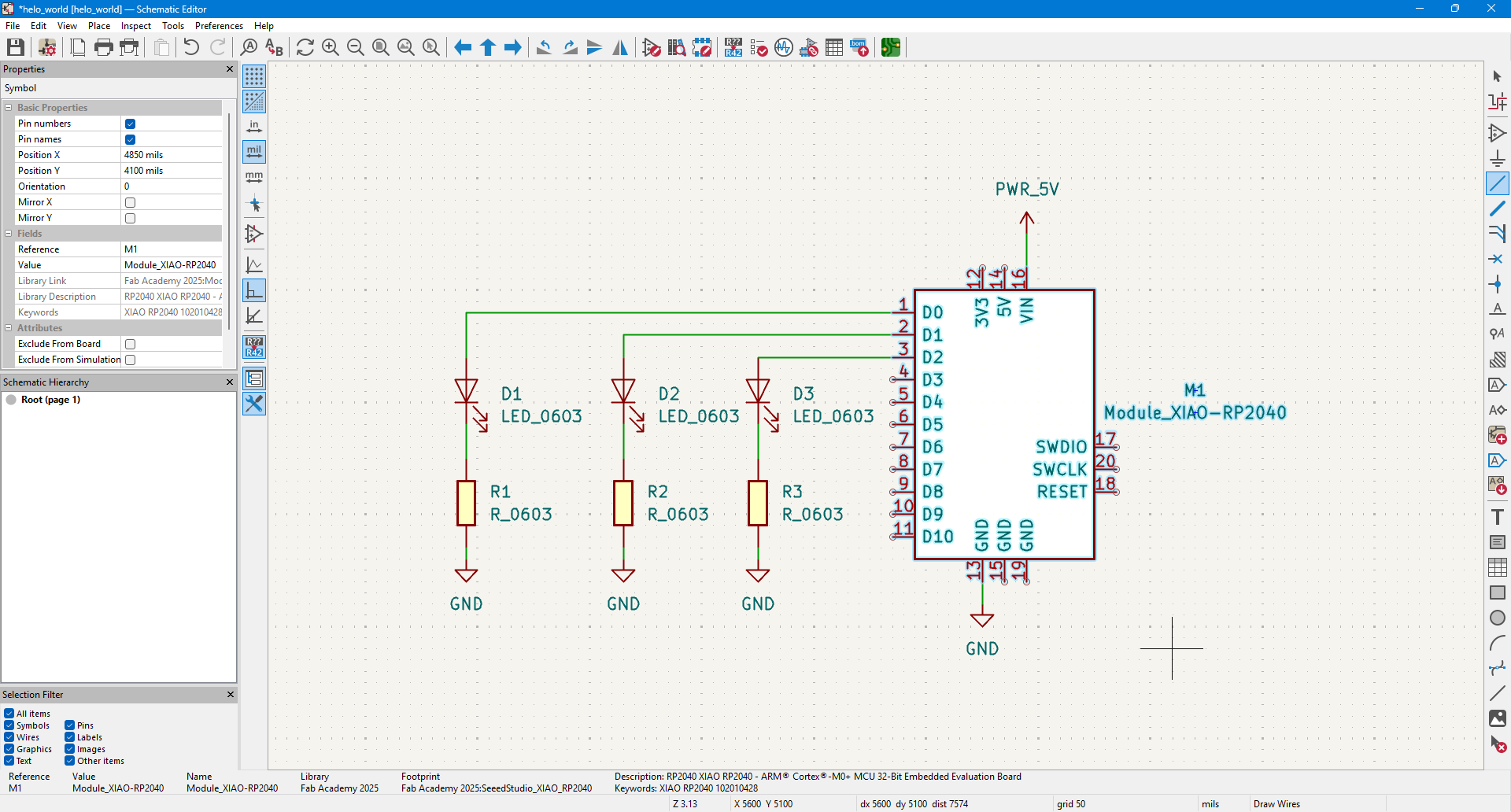
- I started a new project in KiCad and created a schematic for my PCB.
- The design included the RP2040 microcontroller and LEDs to test basic circuit functionalities.
- I placed and wired components in the schematic editor before proceeding to PCB layout.
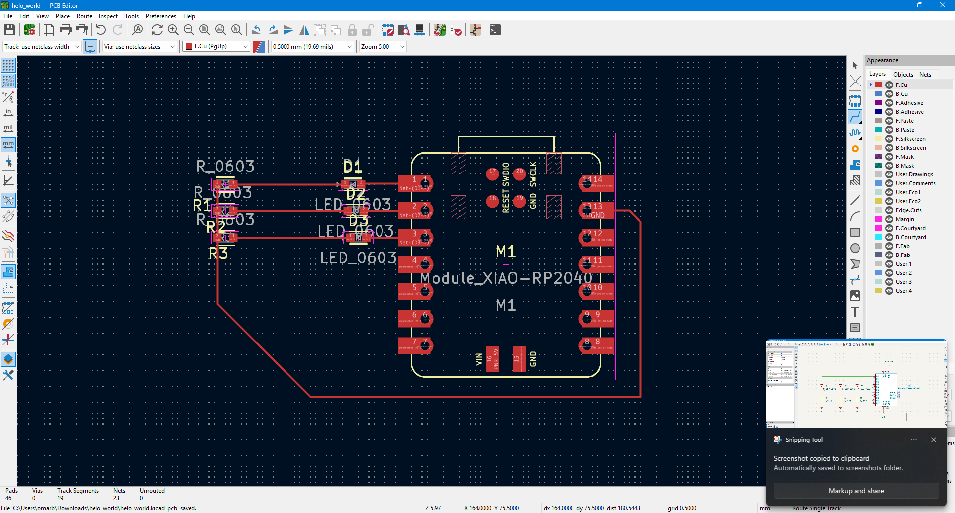
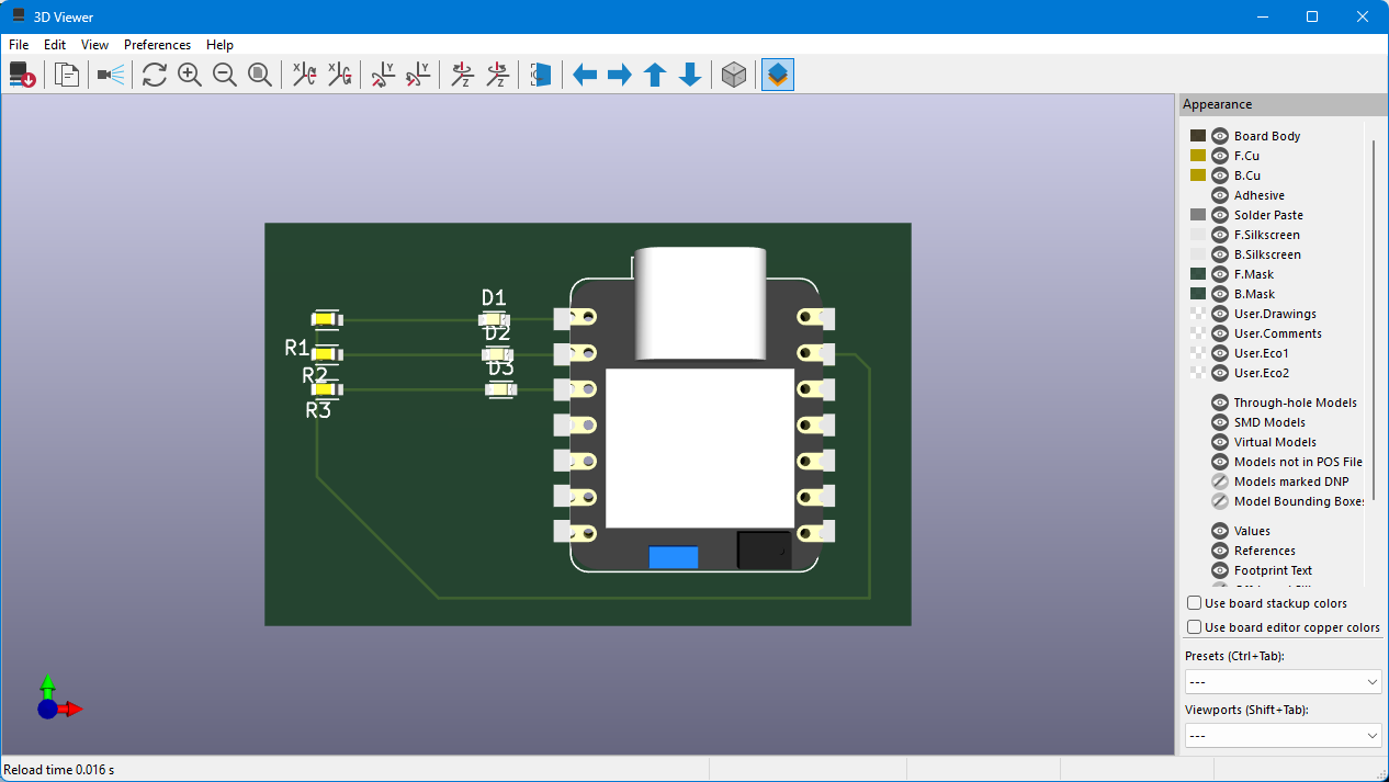
- Once the schematic was complete, I assigned footprints and moved on to designing the board layout.
Learning Outcome
1️⃣ Downloaded and installed KiCad from the official website.
2️⃣ Configured KiCad with the Fab Academy inventory library to access necessary components.
3️⃣ Designed the schematic for a PCB featuring the RP2040 and LEDs.
4️⃣ Laid out and routed the PCB, ensuring proper electrical connections.
5️⃣ Ran a Design Rule Check (DRC) to verify the integrity of the design.
This process gave me practical experience in KiCad schematic design, footprint management, PCB routing, and design validation. Moving forward, I plan to fabricate and test this PCB to validate its functionality.
