Week 6
Electronics Design
Electronics design and designing are completely new learning for me. I have developed confidence in electronics components, design, and all about PBC. My favourite IC is NE555P, I have explored a lot about this IC and got inspired about on the projects done using this IC. So I have created a simple blink circuit using NE555P.
Group Assignment
Testing equipment in our lab:
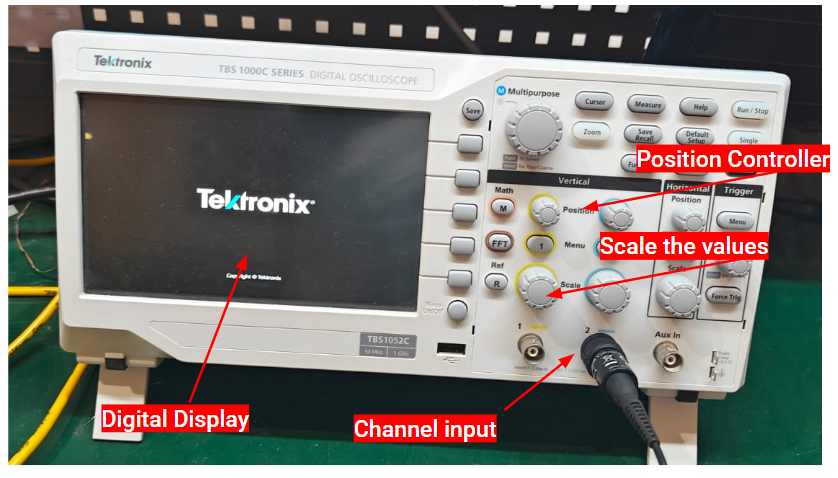
For this week's group assignment, we explored the working of a Digital Oscilloscope.
A digital oscilloscope, also known as a digital storage oscilloscope (DSO), is an electronic instrument used to visualize and analyze time-varying electrical signals unlike older analog oscilloscopes that directly display the waveform on a cathode ray tube (CRT), a digital oscilloscope samples the input signal and converts it into a digital format for storage and processing.
To understand the working principle, we connected a potentiometer and an LED to the oscilloscope. We were able to see the working of the variable resistor controlling the voltage with the brightness of the LED, and also the values in the digital display.
Individual Assignement
For individual assignment this week, I have created my favorite NE555P Blink circuit. Along the process, I have used KiCAD to design the circuit and various plug-ins available in KiCAD. For reference, I have used the following circuit inspired from the internet
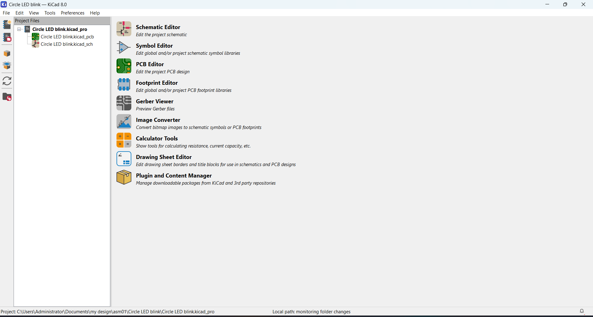
KiCAD
KiCad is a powerful, free, and open-source software suite for electronic design automation (EDA). 1 It enables the creation of professional-grade schematic diagrams and printed circuit board (PCB) layouts. 2 With its comprehensive set of tools, including a schematic editor, PCB editor, 3D viewer, and Gerber file generator, KiCad supports the entire design workflow from concept to manufacturing. 3 Its cross-platform compatibility and active community make it a popular choice for hobbyists and professionals alike.
Suggested to download KiCAD 8.0
Fab KiCAD Library Download Link
Github Fab Academy Resources
To Learn more about KiCAD
YouTube link for Fab Foundation Tutorial
Here is how I created the Blink Circuit using NE555P
Open KiCAD and start a New Project from the files menu -> You will see a Schematic and PCB file created in the model tree. Next, open Schematic to start drawing a schematic of our circuit |
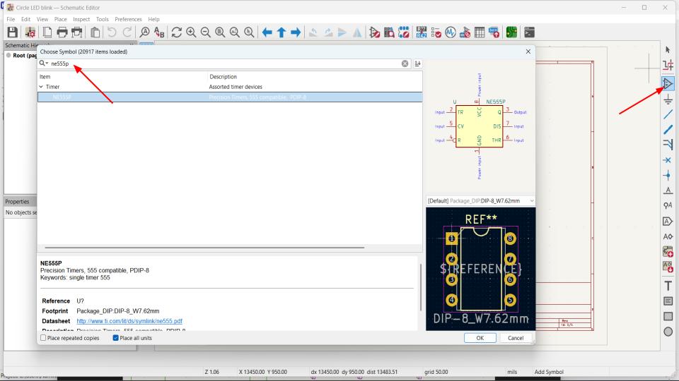
In schematics, click - Add Symbols, In search tab look for NE555P and insert it, you fill find the schematics and footprint |
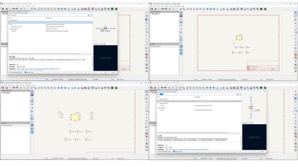
Similarly, add LED_1206, R_1206 (Resistor), and C_1206(Capacitor). For my requirement, I have added four LEDs and Resistors, and 2 capacitors. |
Connect all the components as per the reference sketch and complete the circuit |
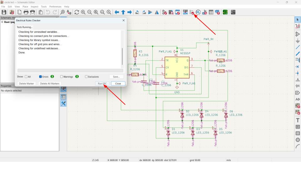
For Electrical Rules Checker, click the icon from the top ribbon menu and click “Run ERC” It was very tough to get the schematics correct. After a lengthy trial and error finally got this correct schematics |
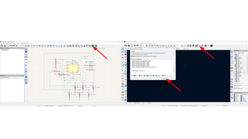
To start designing the PCB circuit, click on the open PCB design icon in the schematics window, and a new PCB design window will open. Click “Update PCB with changes made in the schematics,” and you will find the footprint of all the components that have been added in the schematics. |
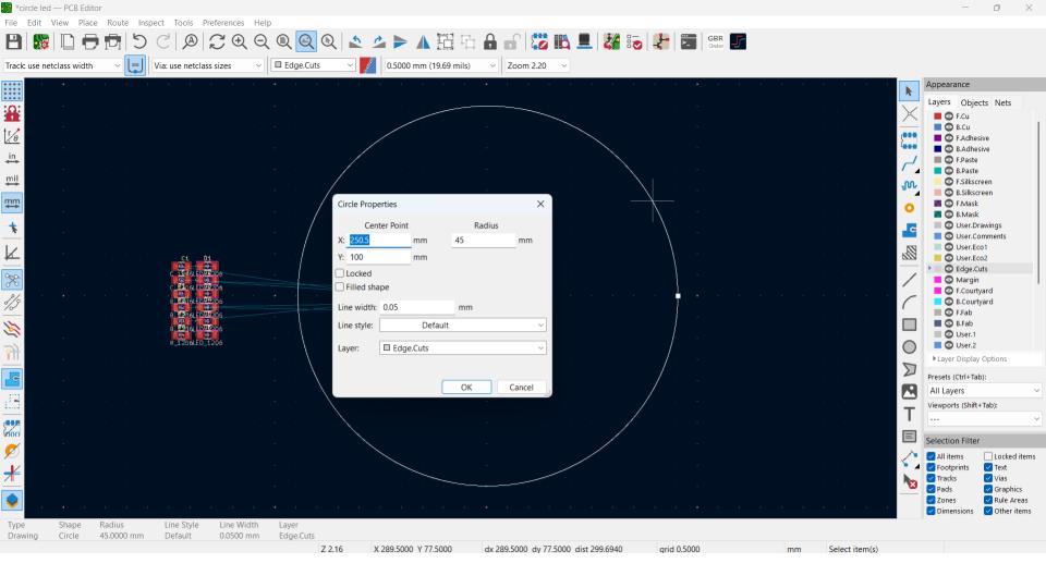
For reference, I have added an Edgecut - Circle, which gives a reference for the PCB size, and it will help us to have the tracks inside the Edge cut track. |
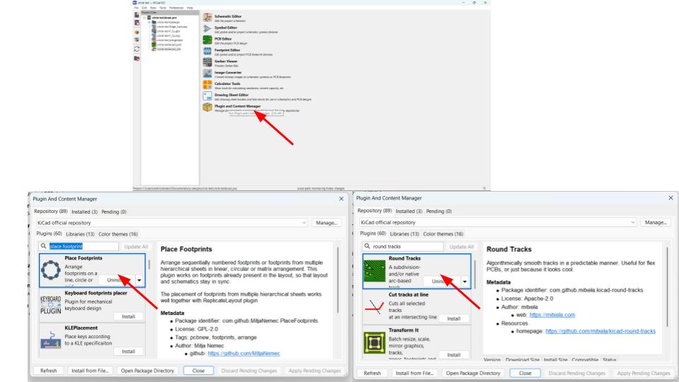
Add some useful plugins
|
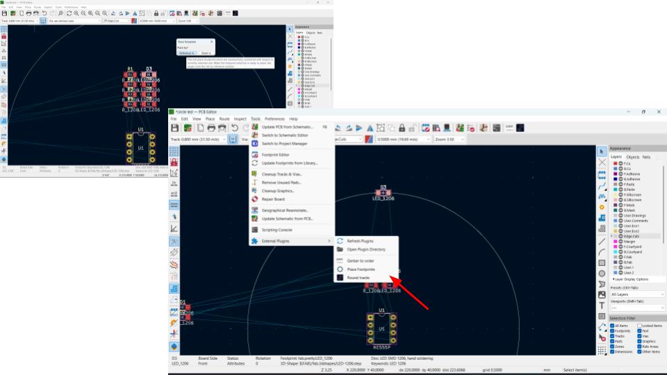
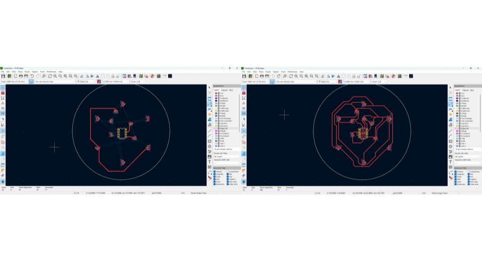
The plugins can be accessed from the Tools -> External Plugins -> Place footprint Using this option, I have placed all the LEDs and Resistors in a circular array. Since I have used only 4 LEDs and Resistors, it looks very normal. If you increase the numbers, you will good circular array |
Start connecting all the components using a track width of 0.6mm and complete the circuit. Experiment with the lines and also passing through the resistors. It was great fun in connecting the components. |
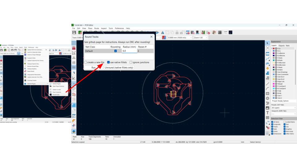
To convert the straight line tracks into rounded tracks, select the “Round Track” plugin from Tools -> External Plugin Define the radius to the required radius value. It will be fun to try different radius values. |
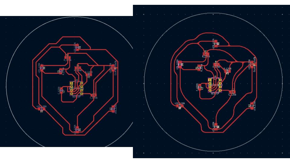
Comparison between the straight line and the rounded tracks. |
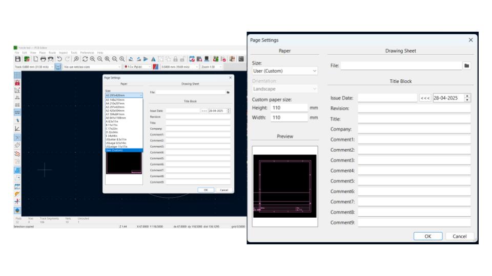
To extract the tracks, change the page settings to custom size and move the design into the page created. |
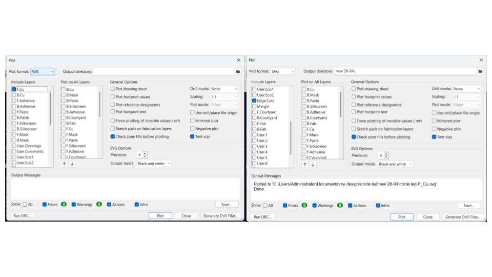
Using the plot command from the files menu, extract the SVG format of F.Cu and EdgeCuts. Don't forget the select the mirrored plot option link as I missed in this image. |
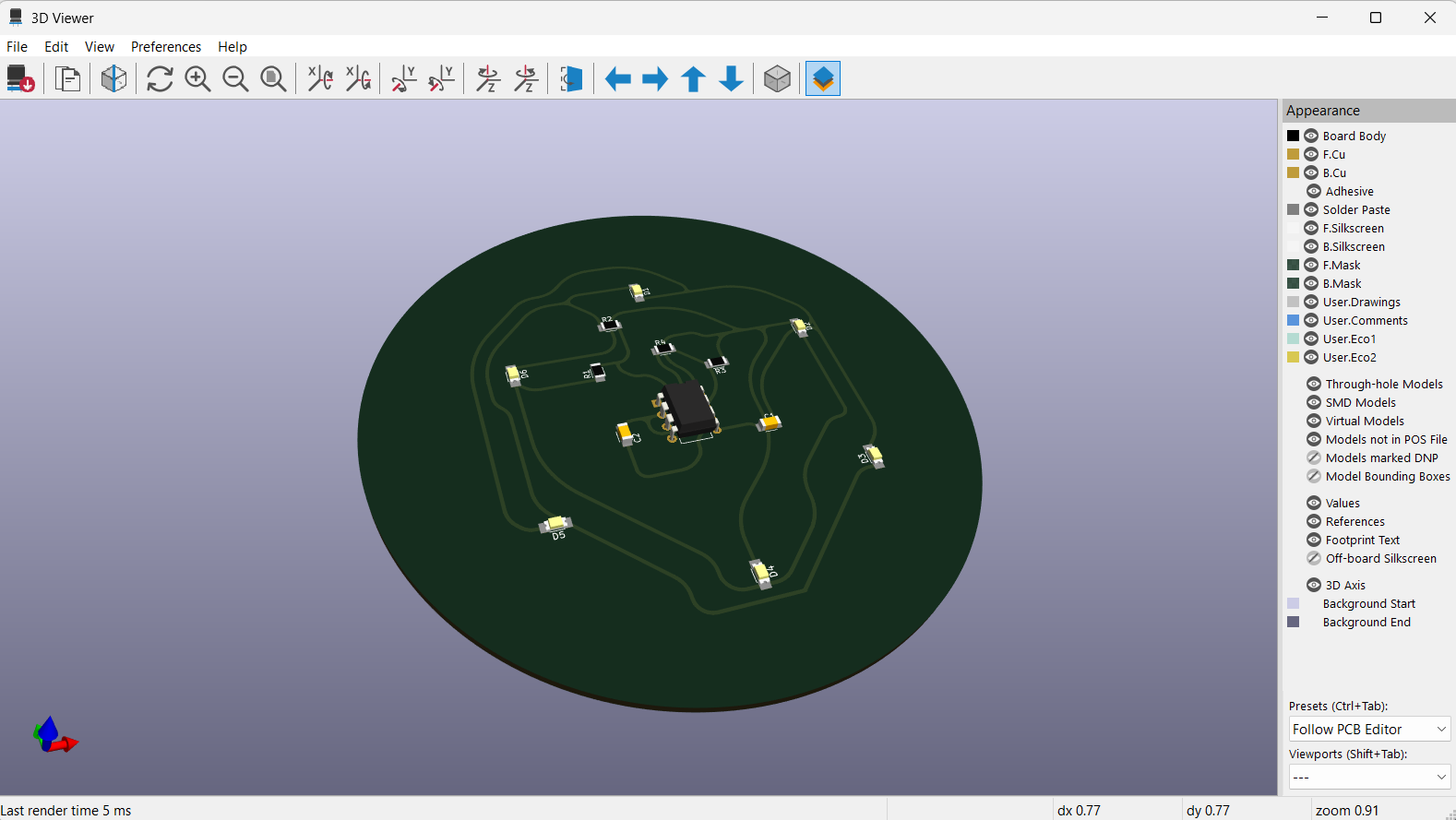
Click in 3D view to view the rendering of the circuit we designed. We can see the components and the tracks in the 3d view. |
Source Files: