PCB DESIGNING
This is the 6th week and it is going to be covering PCB designing.
I started by making research on the software that is going to be good while designing and I found that we have KICAD, solidworks AND EASYEdA and I choosen EASYEDA because it is very easy to interact with the components and it is very easy to access the datasheets of components
Description of group assignment
-
Use the test equipment in your lab to observe the operation of a microcontroller circuit board (as a minimum, you should demonstrate the use of a multimeter and oscilloscope)
-
Document your work on the group work page and reflect what you learned on your individual page
-
Use an EDA tool to design a development board that uses parts from the inventory to interact and communicate with an embedded microcontroller
Goup assignment
Individual assignments
Group assignment
In this week Electronics Design Group assignment,I explored the operation of a microcontroller circuit board using test equipment such as a multimeter and oscilloscope. Through our group assignment link, we analyzed circuit behavior, measured voltage and signal patterns, and gained a deeper understanding of debugging electronic circuits. This hands-on experience helped me improve my skills in circuit analysis and troubleshooting.
Individual assignment
installation of software I will be using
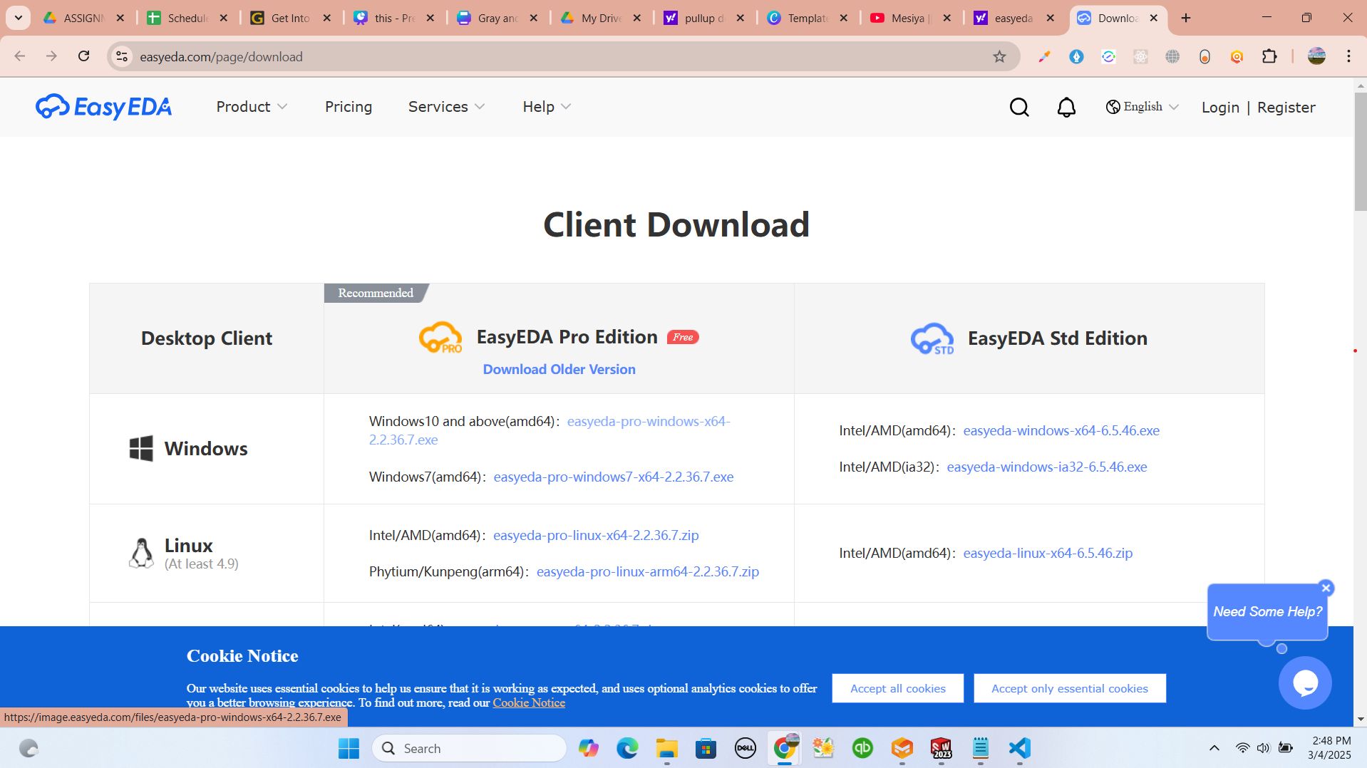
this is how I downloaded EASYEDA
here is the link which I used to download the easyeda for pcb designinghttps://easyeda.com/page/download
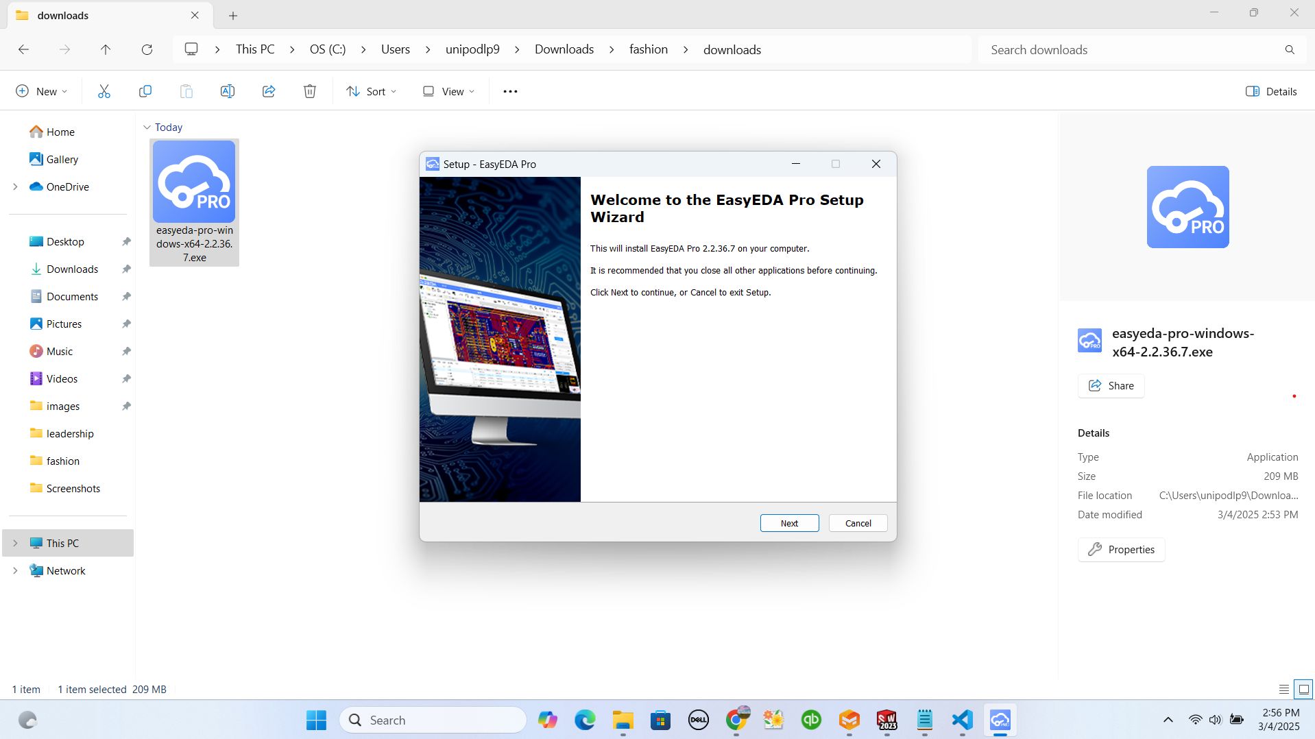
after downloading the easyeda software, I installed and created account which I will be using while sharing access on my working space and the files and also to help me to access my saved files either local and online
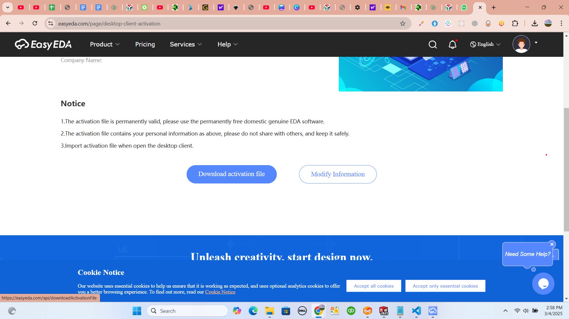
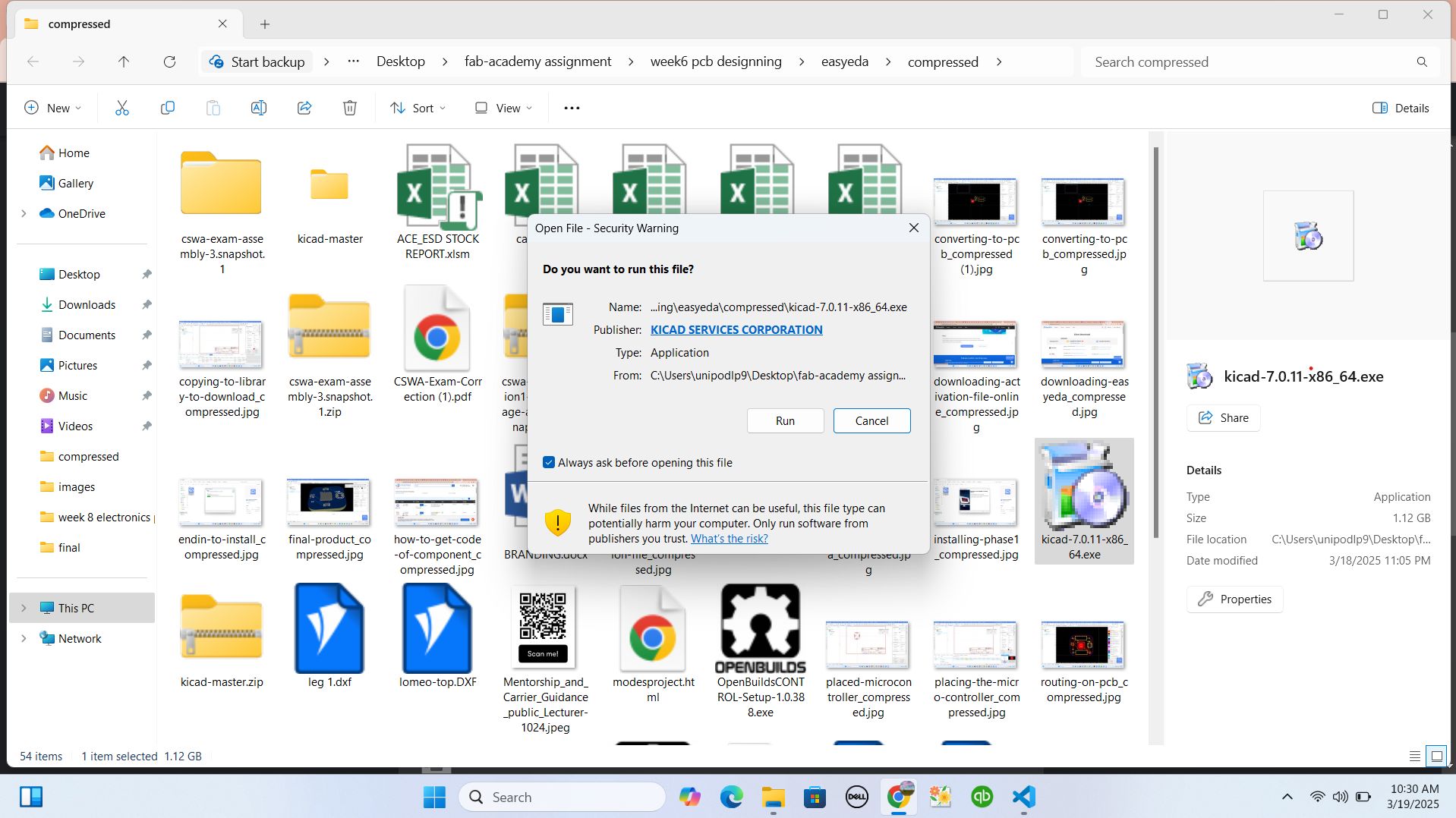
while installing easyeda, the software prompted me to have an activation file and I gone through the process of downloading it
then I clicked on the provided link directing me to website where I should download the activation file
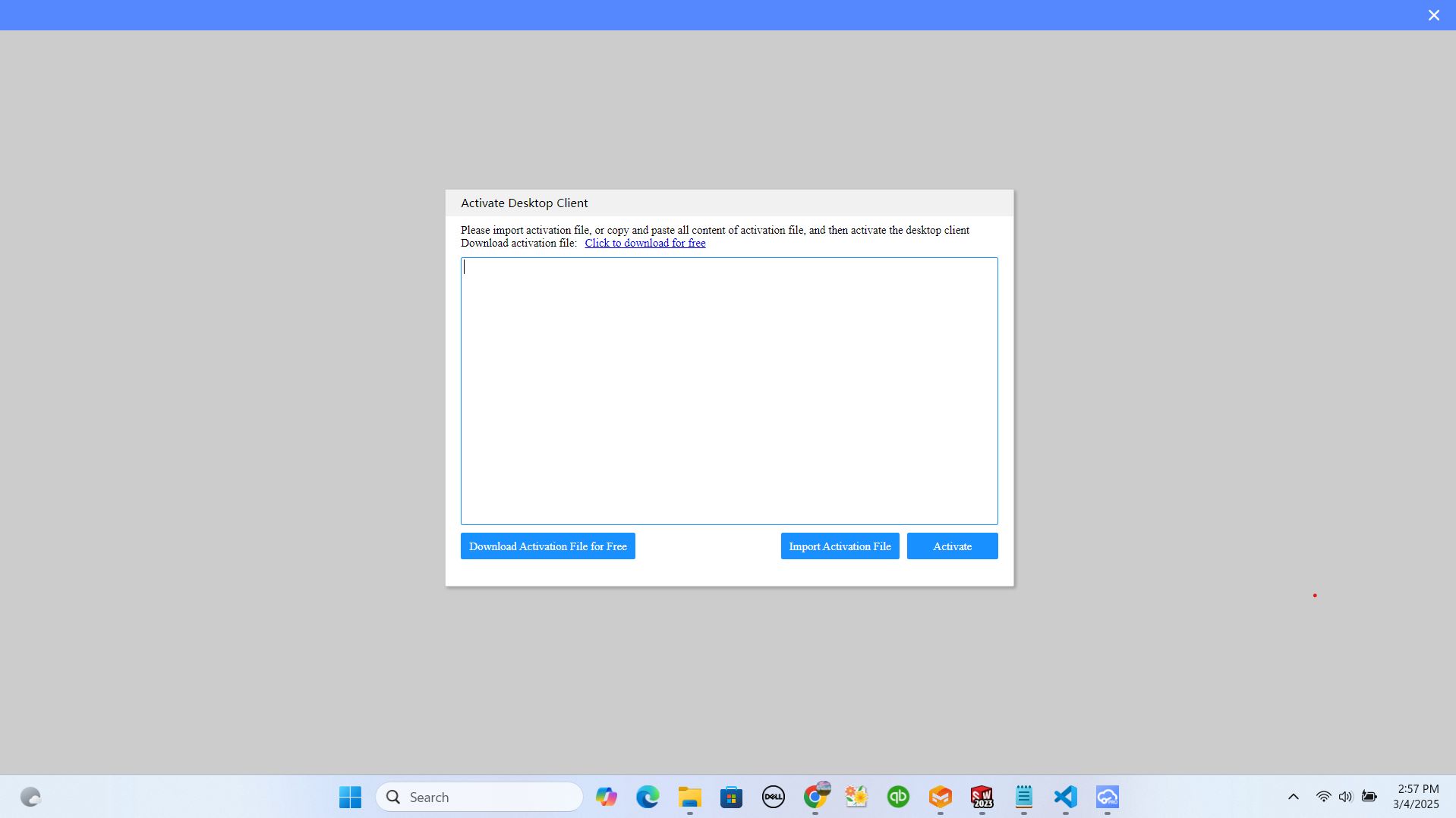
by here I clicked on the button named download activation file
after downloading, I imported the activation file to my intaller
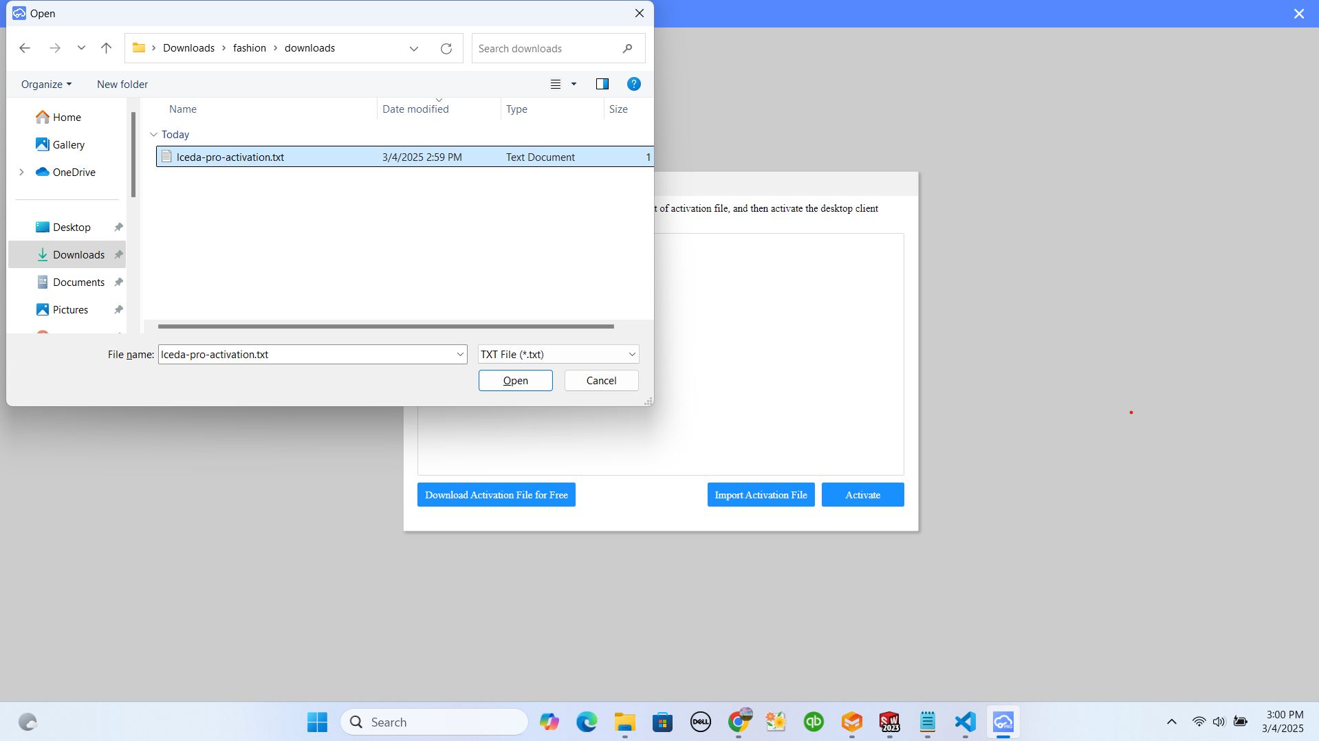
after importing the file, I cliced on activate button
by here I can't share personal info on my site because the activation file contains personal data
after importing and activating the software, the installer continued to the final step and now the software is ready to be used and I opened it
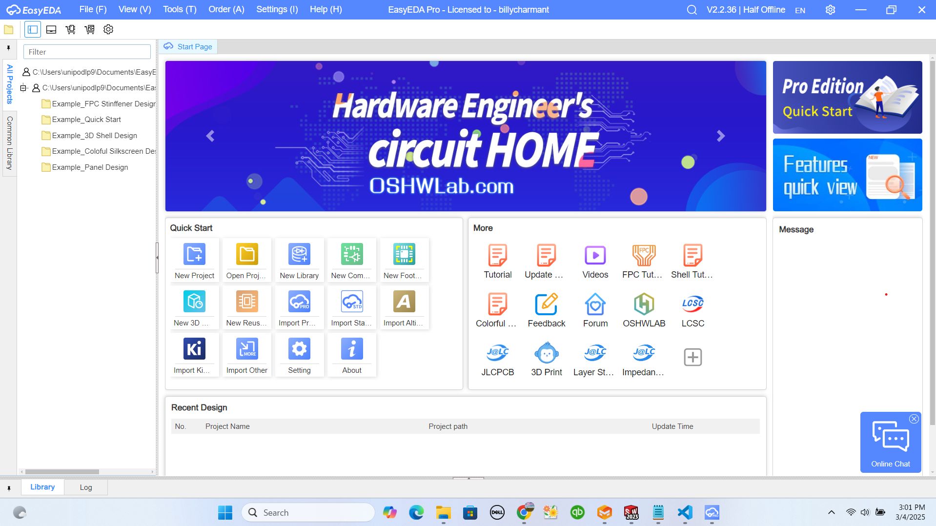
on the interface, I found the option of opening new project and I selected it and it given me the interface which is composed of schematic part for designing, sidebar where I will be getting components in libraries, top nav-bar with different features and tools to be used while designing and footer where I will be using to import other libraries
I had an idea to desing PCB that will help me to build my project where I will be measuring the temperature and track the cow's location
I started by searching the components I should use and I realised that some of them are found locally and others needs to be imported from online store of the components
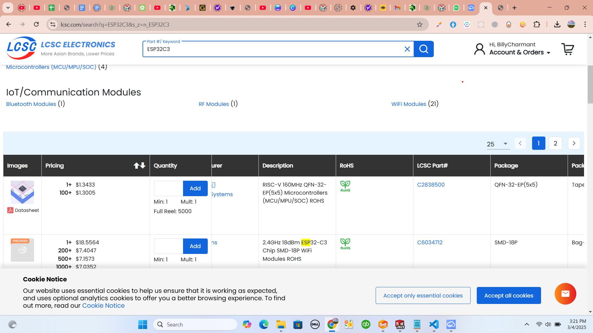
here is the link which I used while downloading and importing tools to be used in my pcb designinghttps://www.lcsc.com/
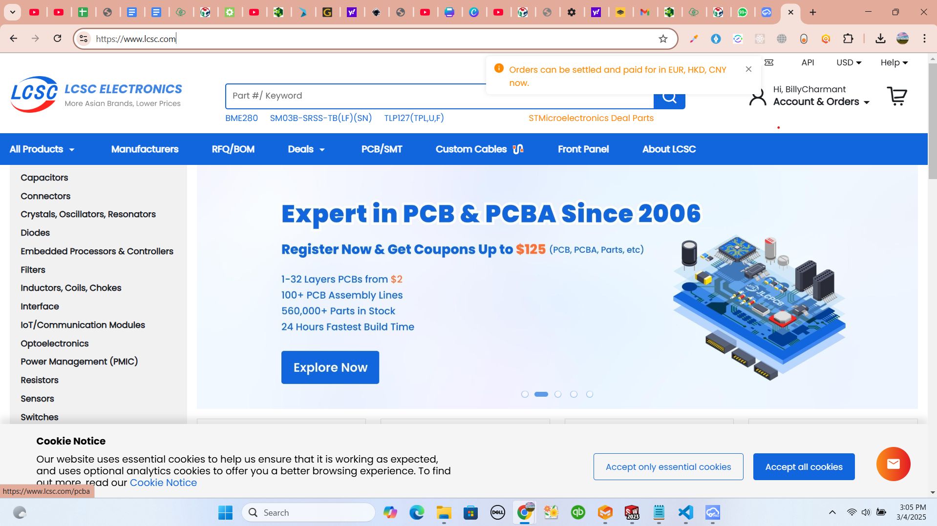
by here, I started by navigating into store checking if there is available components according to what I want to use.
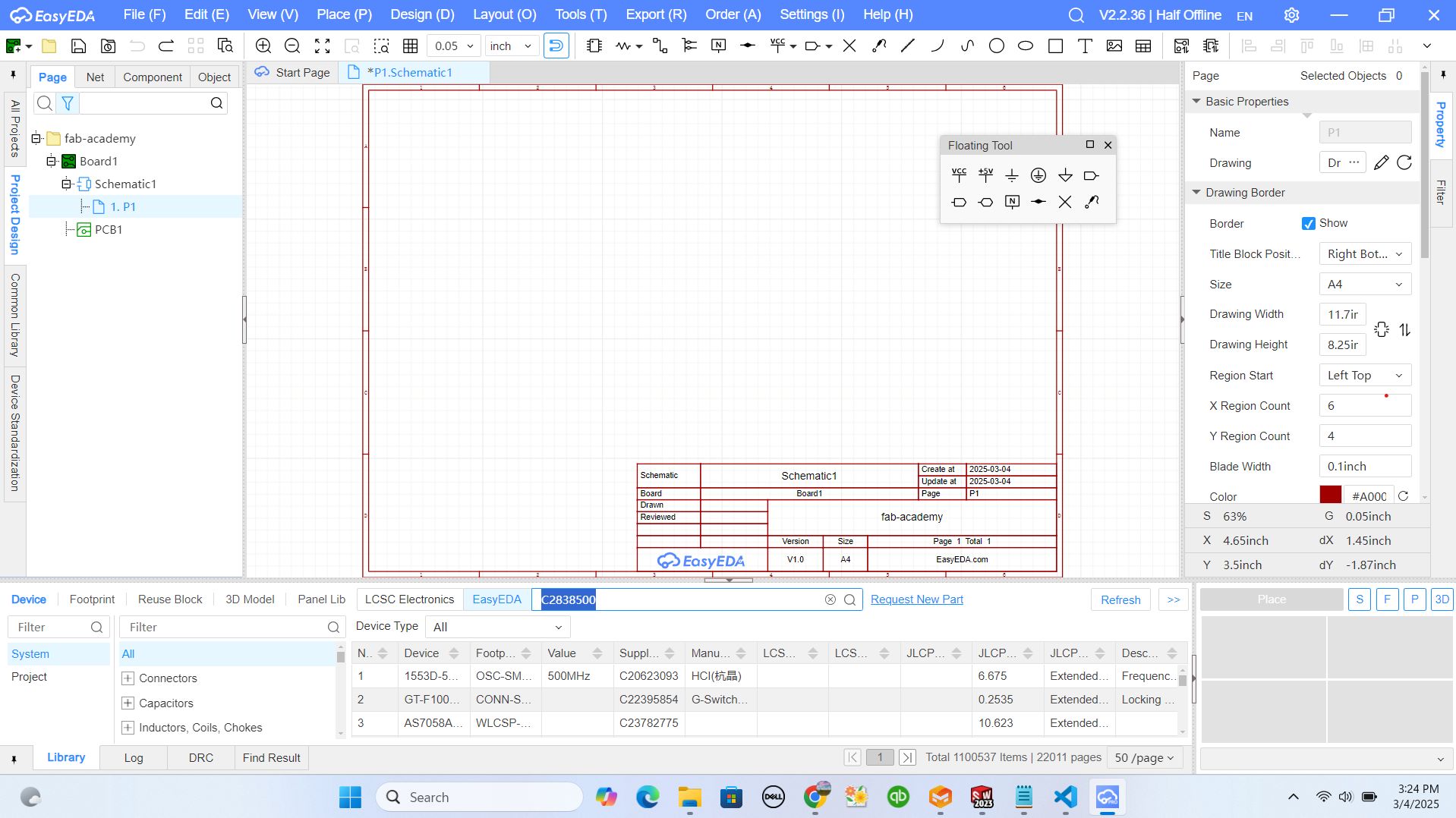
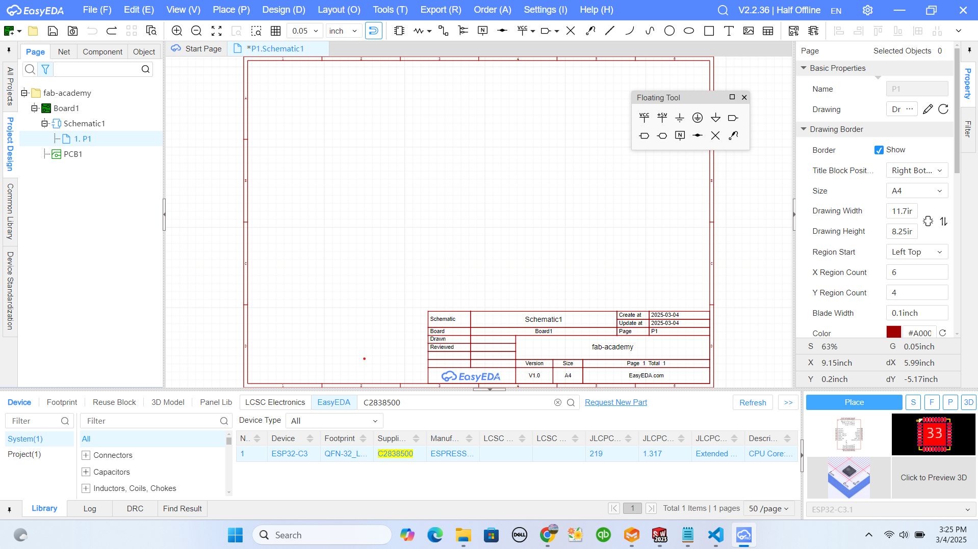
I selected the components that meets with creteria I wanted in my PCB and it was ESP32C3
after I copied the code of the component and I pasted it into my local app to download them in local app and installed the components into library folder
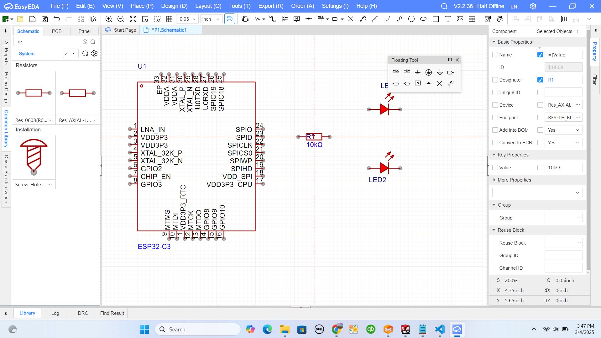
after getting the components like microcontroller from the step of downloading them from store, I started to add them in my schematic designing part and I added other components like resistors and LED to get my design connected and designed
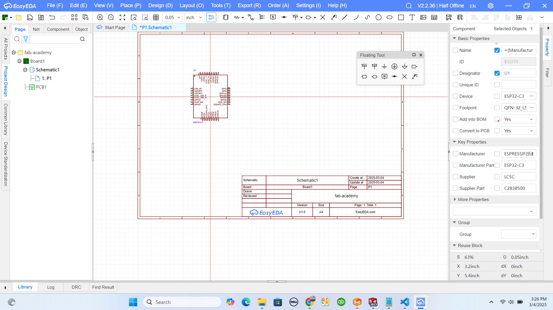
after adding the microcontroller, I added other components like LED and resistors from locall library to help me building my PCB as I want.
adding and connecting LED to the micorcontroller in the design
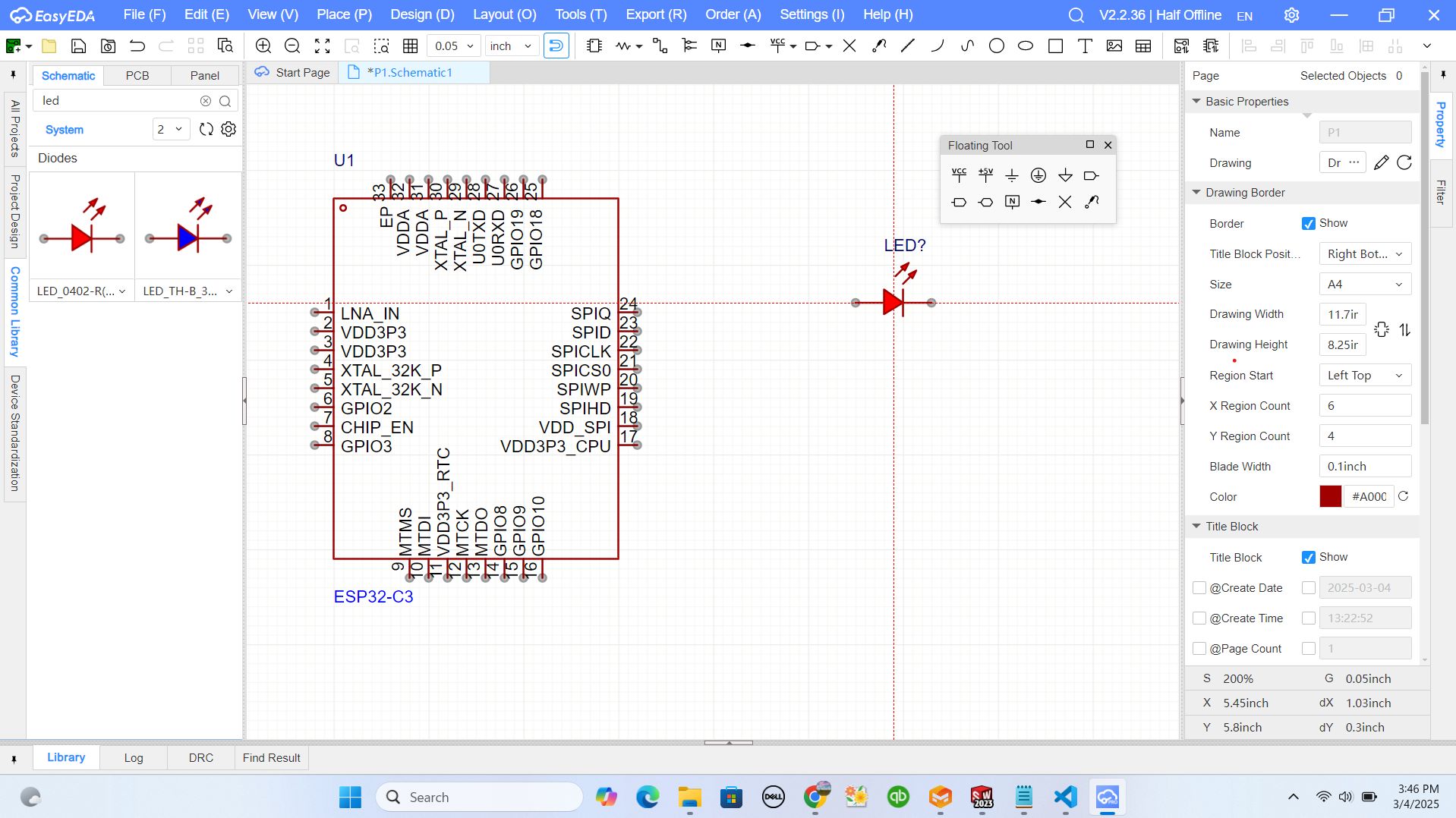
adding and connecting resistors to my design
after adding all components I choosen to use, I converted the schematic design to PCB design part
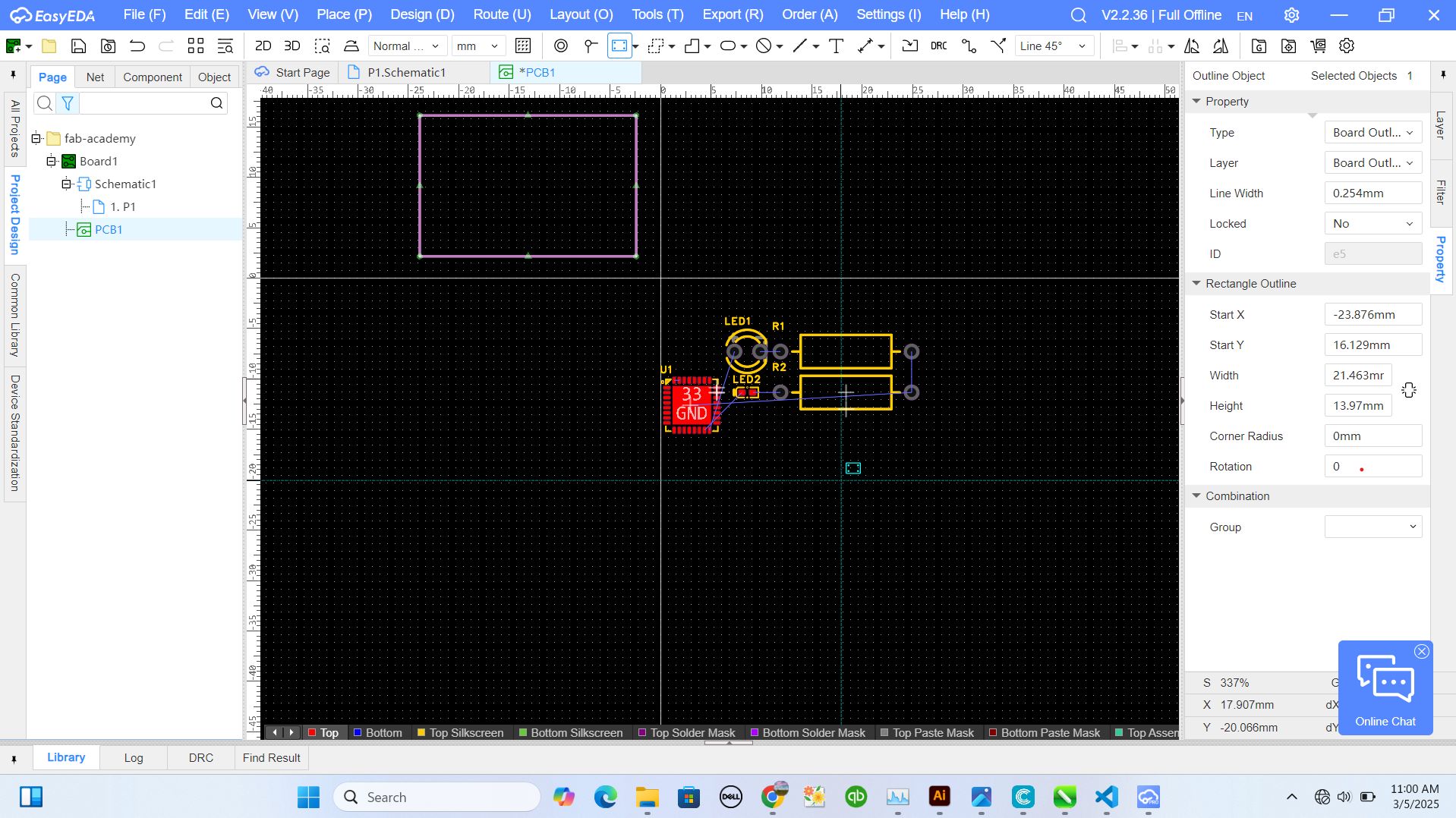
on this stage, I arranged the components and built the frame for my pcbwhich is board outline and I allocated the microcontroller in the center of the frame to help all components to have access easily getting connected to microcontroller respecting the height and the width of board outline
after that I used Routing feature by creating the lines where the flow of current will be passing by respecting to connectivity
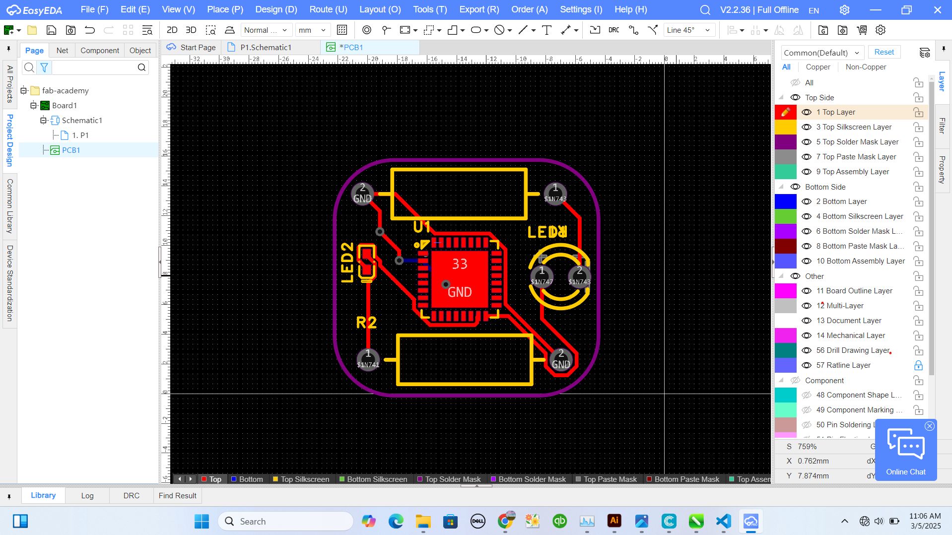
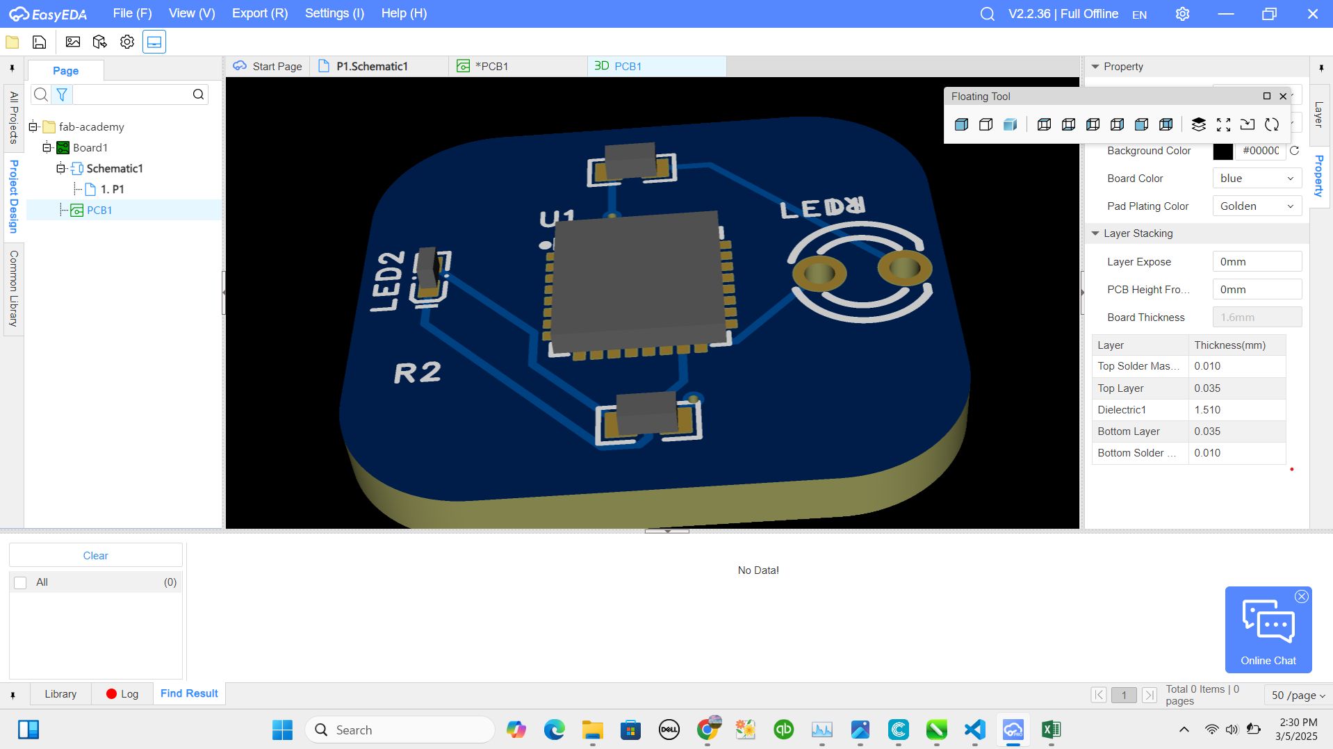
by here my pcb was able to be converted to 3D view and 2D view where you see how it will be looking like while printing
KICAD Software
this is how I downloaded and installed KiCad
To start designing the PCB, I installed KiCad, an open-source PCB design tool. Downloading the software from kicad.org was straightforward. After installation, I explored the interface to familiarize myself with its tools.
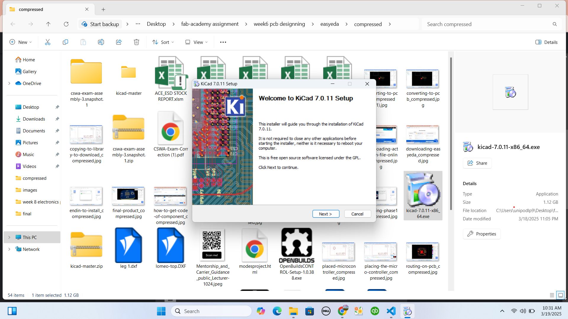
after downloading the kicad and installed, I opened it and started to use it
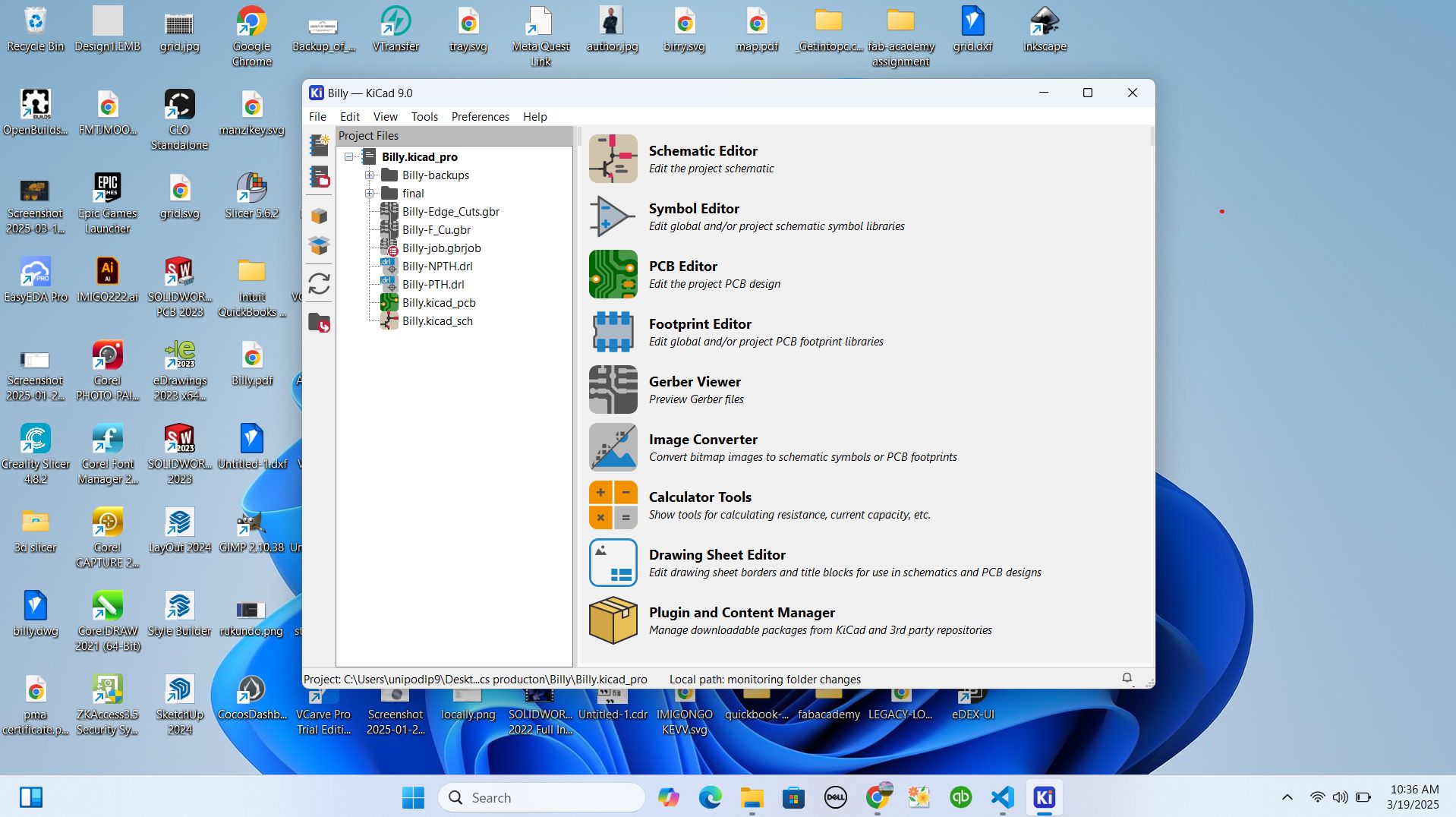
Creating a New Project
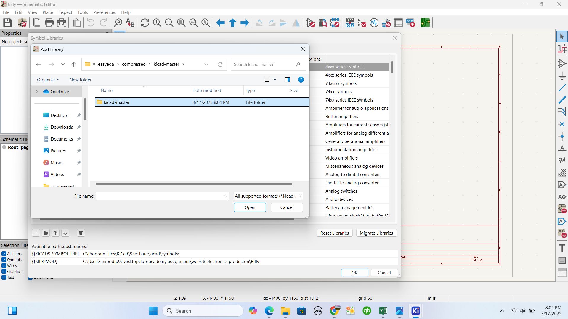
while I was trying to open the microcontroller recommended by Fab-lab, I found that it is missing and I started to import the library from fablab gitlab via https://gitlab.fabcloud.org/pub/libraries/electronics/kicad
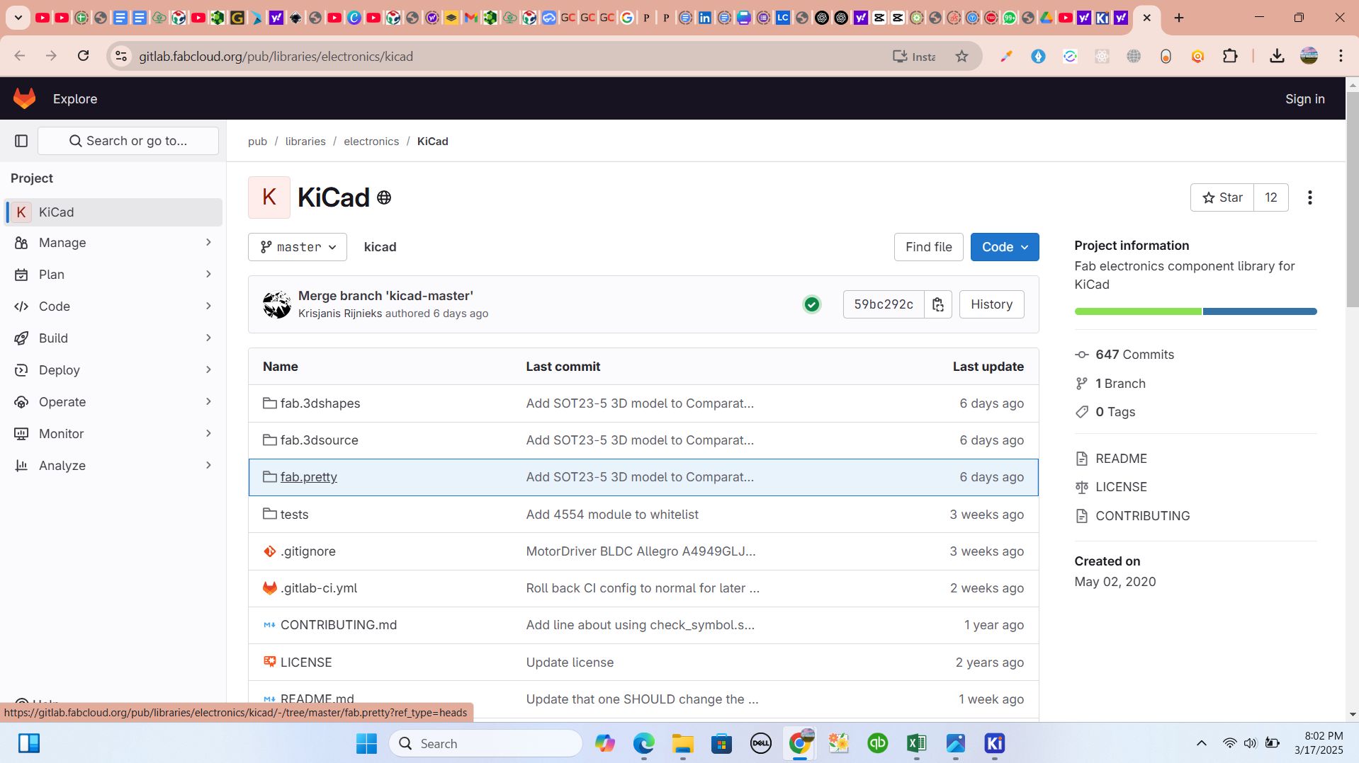
after, I imported the library into the Kicad libraries to be used as other libraries
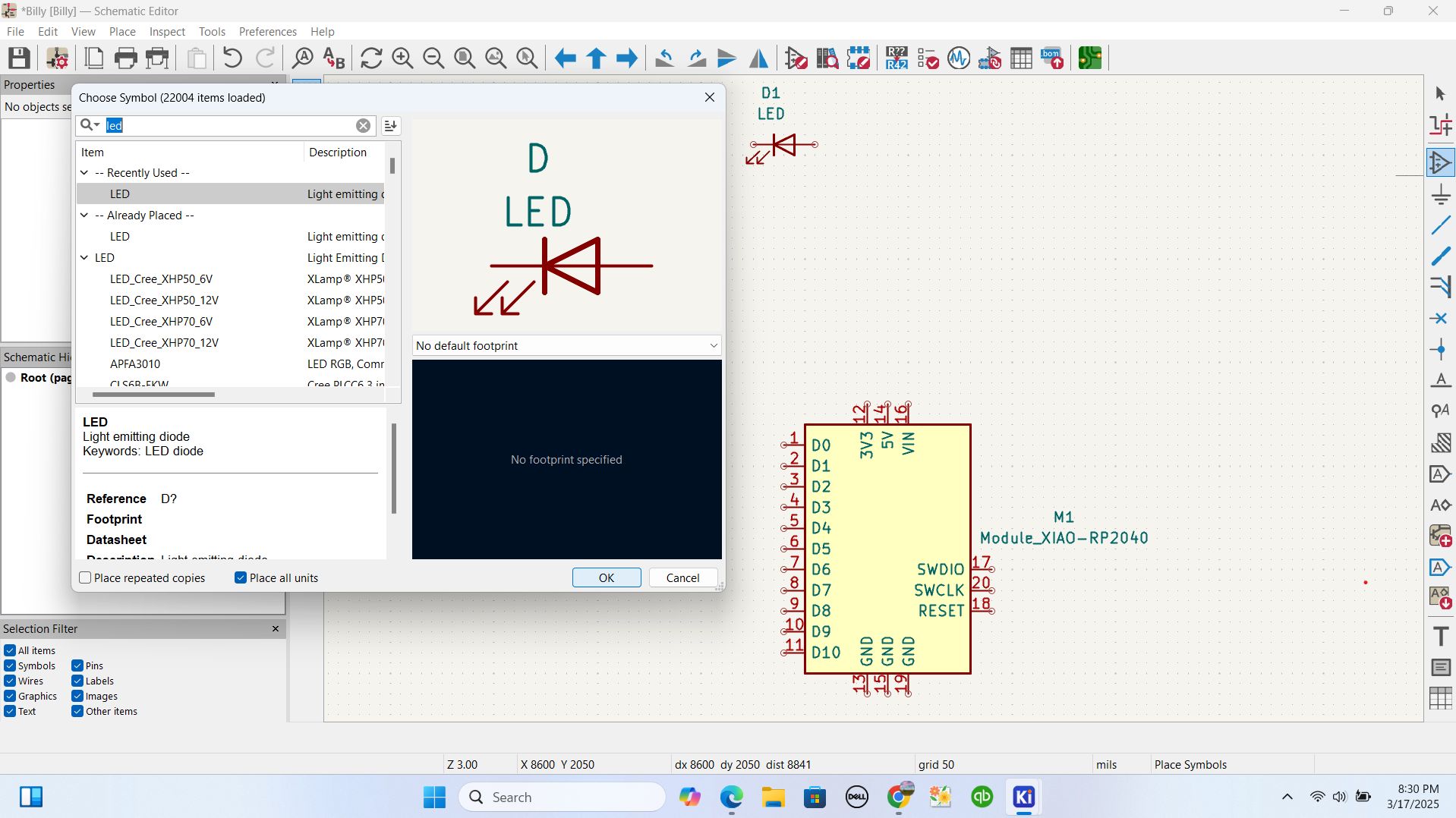
I created a new project and named it Billy.pcb and opened schematic editor to place tools and components. This project would hold all the necessary schematic and layout files where I started by adding microcontroller and LED
after that I added resistors and ground and also connectors where it connects the ports and the components
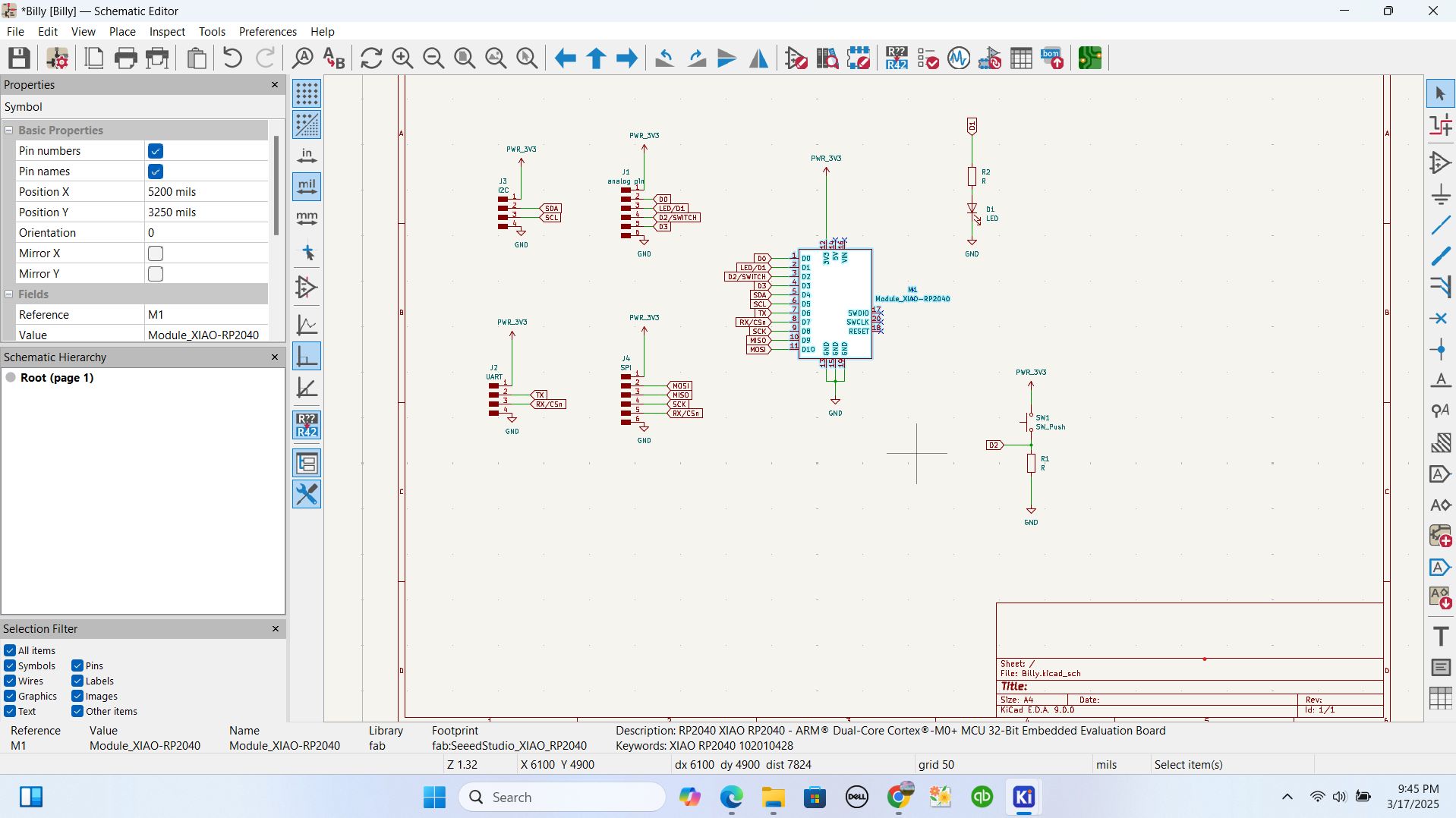
by here, I was ready to convert my schematic design to pcb but is started by assignnig the footprint on my design to connect the components and the ports
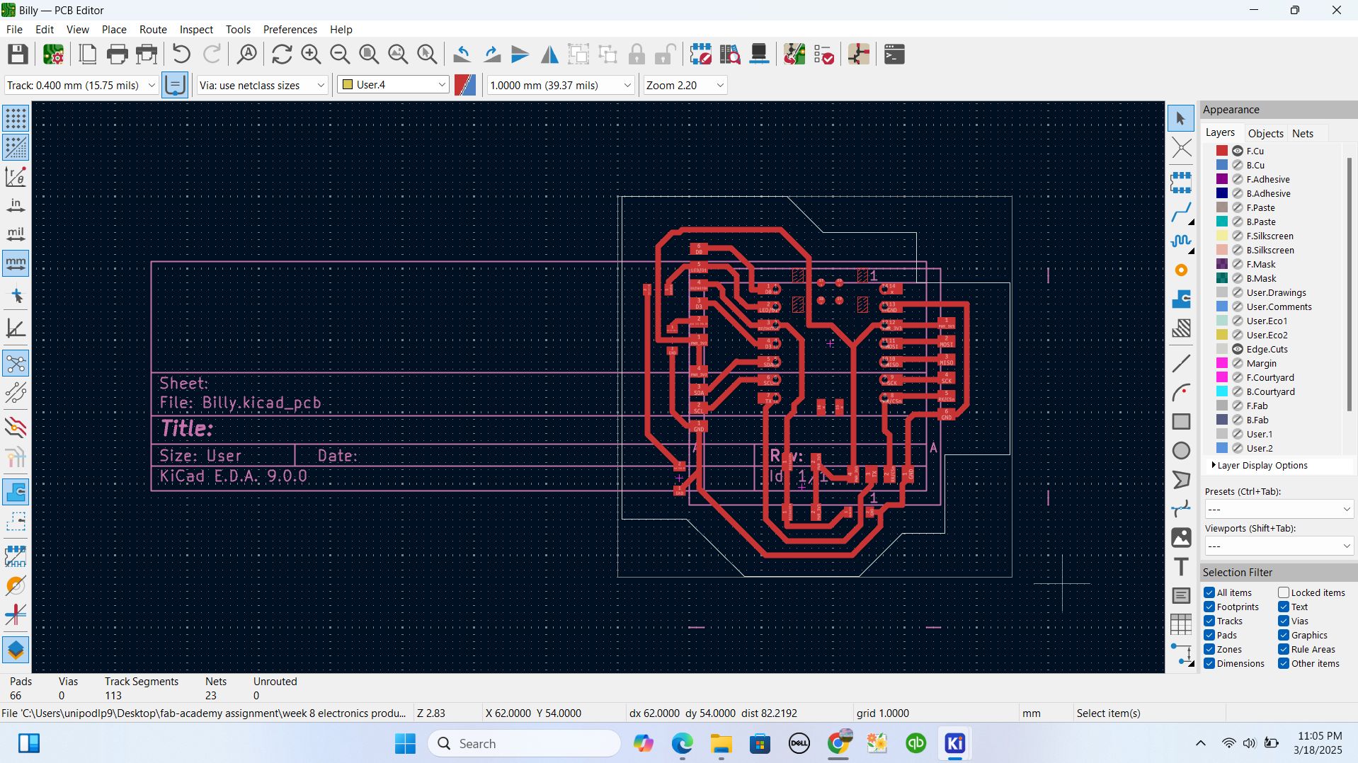
by this step, I made clear lining and measuring the thickness of the line. I changed the view of the the layout to 3D
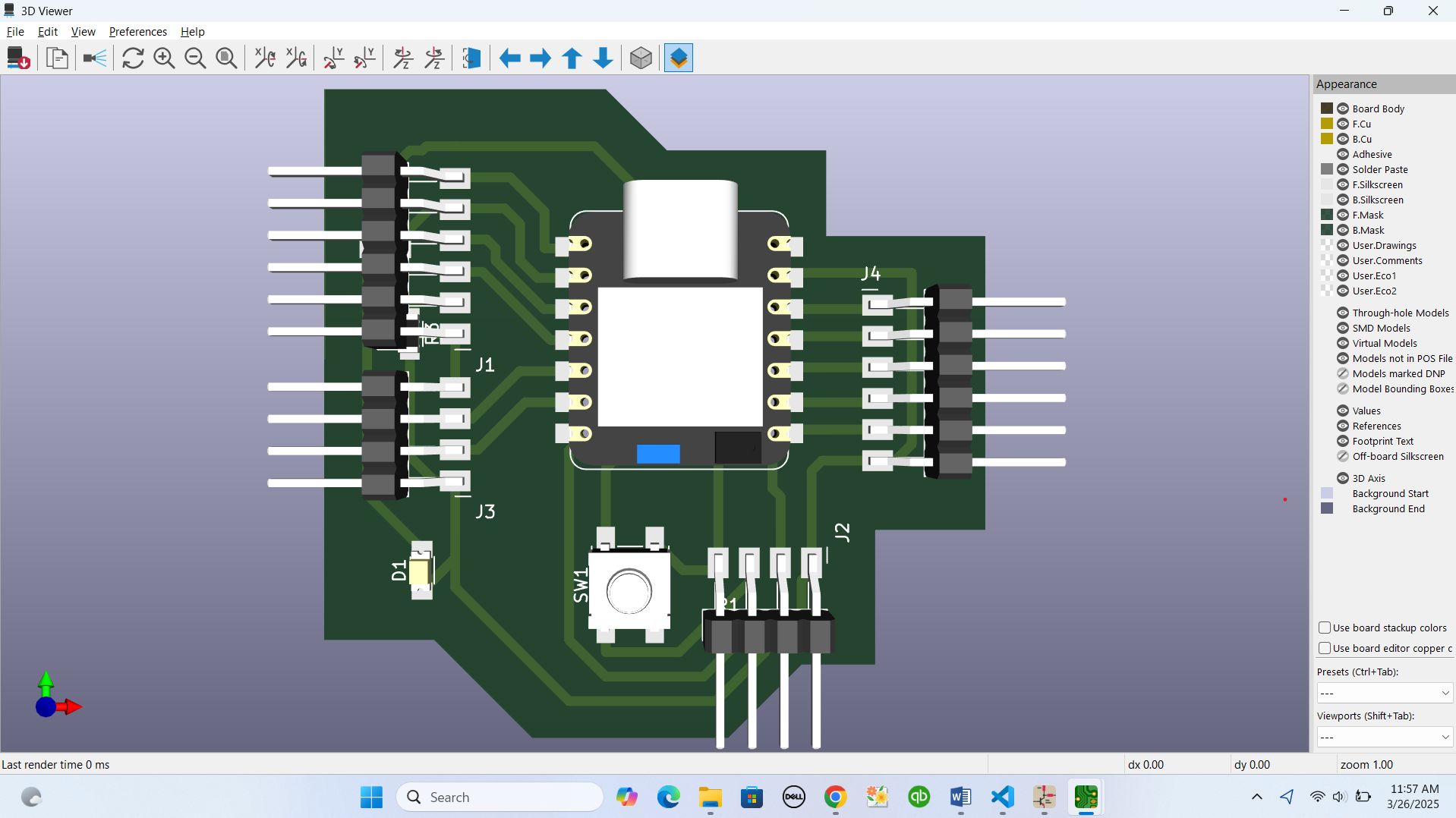
Here is the original files
PCB design Using KICAD
PCB design of my project in KICAD